EP0455090A1 - Integriert optische Komponente und Verfahren ihrer Herstellung - Google Patents
Integriert optische Komponente und Verfahren ihrer Herstellung Download PDFInfo
- Publication number
- EP0455090A1 EP0455090A1 EP91106456A EP91106456A EP0455090A1 EP 0455090 A1 EP0455090 A1 EP 0455090A1 EP 91106456 A EP91106456 A EP 91106456A EP 91106456 A EP91106456 A EP 91106456A EP 0455090 A1 EP0455090 A1 EP 0455090A1
- Authority
- EP
- European Patent Office
- Prior art keywords
- grooves
- waveguides
- central part
- longitudinal grooves
- substrate
- Prior art date
- Legal status (The legal status is an assumption and is not a legal conclusion. Google has not performed a legal analysis and makes no representation as to the accuracy of the status listed.)
- Granted
Links
Images

Classifications
-
- G—PHYSICS
- G02—OPTICS
- G02B—OPTICAL ELEMENTS, SYSTEMS OR APPARATUS
- G02B6/00—Light guides; Structural details of arrangements comprising light guides and other optical elements, e.g. couplings
- G02B6/24—Coupling light guides
- G02B6/26—Optical coupling means
- G02B6/30—Optical coupling means for use between fibre and thin-film device
Definitions
- the present invention relates to an integrated optical component and its manufacturing process.
- the so-called integrated optics technique allows the creation of waveguides in a dielectric substrate, generally made of glass, by local increase in the refractive index of the glass. It uses ion diffusion methods or methods of depositing suitable layers on the substrate.
- document FR-A 2612 301 discloses an integrated optical component, the glass substrate of which comprises a central part in which the waveguides are created and the two lateral parts of which share and 'other of this central part have fiber positioning grooves and fiber release grooves.
- the substrate with its fiber positioning grooves is made from precision molding.
- the waveguides are made in the central part of the substrate, aligning their ends with the fiber positioning grooves already existing on the substrate.
- the fiber release grooves are made transversely to the positioning grooves and to the guides, preferably after formation of the guides, by mechanical machining. They are on either side of the central part being adjacent to the ends of the guides to define with this central part, on each side of it, an interface shoulder for connecting the fibers to the waveguides.
- Positioning grooves allow rough alignment of the bare fibers they receive individually with the ends of the waveguides and the substantially contacting of the ends of the fibers against the corresponding interface shoulder. The fibers being thus positioned, they are held in their positioning grooves and sealed to the substrate using glue while their ends at the clearance grooves remain free.
- the release grooves then make it possible to obtain the final precise alignment of the fibers with the waveguides, before sealing the ends of the fibers against their interface shoulder.
- This final precise alignment is ensured using a micromanipulator, the gripping element of which can grasp the free ends of the fibers in the space provided by each clearance groove.
- This final adjustment compensates for the lack of sufficient precision of alignment, which is difficult to obtain, of the waveguides with the positioning grooves resulting from molding of the substrate.
- the clearance grooves provided to leave the ends of the fibers free and for their final adjustment micromanipulation, do not, however, allow good mechanical strength of the fibers, once the alignment has been obtained and the seal has been obtained. final of their ends achieved. This final sealing becomes fragile: it makes it difficult to remove the micromanipulator engaged on the ends of the fibers and remains very sensitive to the surrounding conditions, all the more so since the final adjustment by the micromanipulator was relatively large.
- the present invention aims to avoid these drawbacks.
- the substrate also comprises second longitudinal grooves, each aligned with one of the first grooves which it extends to the edge of the substrate and of section greater than that of this first longitudinal groove.
- FIG 1 there is shown a glass substrate 1 of parallelepiped shape, on one of the surfaces of which are made the various constituent parts of the integrated optical component according to the present invention.
- This substrate has in its central part waveguides 2 produced in integrated optics.
- these waveguides constitute a Y coupler with a common branch 3 to which two other branches 4 and 5 are joined together.
- This central part of the substrate is designated by the reference 6.
- This substrate also has, on its lateral part on the side of the common branch 3, a first and a second transverse groove 7 and 8 parallel to each other and transverse to the branch 3 and with a rib 9 between them.
- the groove 7, the closest to the branch 3 has its vertical edge, opposite the rib, on which the end of the common branch 3 ends, and which defines an interface shoulder for connecting a fiber to the branch 3.
- the rib 9 is of defined height, made slightly less than that of the central part 6 on the bottom of the grooves 7 and 8, to support the fiber to be connected to the branch 3 when it is placed opposite this branch.
- This substrate also has, beyond the two transverse grooves 7 and 8, a first longitudinal groove 13, aligned with the end of the branch 3 and opening into the transverse groove 8, and a second longitudinal groove 23 extending the groove 13 and wider than it opens on the short side of the substrate.
- the end lateral part carrying these two longitudinal grooves is designated by the reference 16; it is level with the central part 6.
- This same substrate 1 has on its other lateral part on the side of the branches 4 and 5, two transverse grooves 17 and 18, with a rib 19 between them, which are quite similar to the grooves 7 and 8 and the rib 9 between them .
- the edge of the groove 17, other than that belonging to the rib 19, defines an interface shoulder for connecting two fibers to the branches 4 and 5.
- the rib 19 for its part supports these two fibers vertically, as intended for the rib 9.
- two longitudinal grooves 14 and 15 aligned with the ends of the two branches 4 and 5 respectively, and opening into the transverse groove 18 , and two second longitudinal grooves 24 and 25.
- the grooves 24 and 25 extend the grooves 14 and 15, respectively; they are wider than them and open out at the end of the substrate.
- the grooves 13, 14, 15 and 23, 24, 25 are V-shaped grooves; being all from machining, they can have another shape given by the machining tool.
- the transverse grooves 7, 8, 17 and 18 are U-shaped or rectangular.
- FIGS. 2 and 3 illustrate two preliminary processing steps for obtaining the integrated optical component of FIG. 1.
- Figure 2 illustrates the step of creating waveguides 2 on the substrate 1 according to the integrated optics technique, for example using a photoengraving process.
- the substrate is initially with an almost perfectly flat upper surface.
- Guides 2, 3 and 4 are created there, slightly in depth over the entire length of the upper surface free of any grooves at the end of this step.
- Figure 3 illustrates the step of forming longitudinal grooves at the end of the step of Figure 2; it shows in section the substrate 1 with its waveguides 2 and in which the narrowest longitudinal grooves have been machined, which are the groove 13 and the grooves 14 and 15. These grooves are formed, over a fixed length, directly on waveguides already created. Each of these grooves goes to the corresponding edge of the substrate.
- the end portions of the guides obtained at the end of the step in FIG. 1 are therefore directly used as guide marks for the machining tool. These grooves remove the guide portions on which they are drawn and are in perfect alignment with the new remaining end portions of the guides.
- the grooves thus produced extend towards the middle part of the substrate, slightly beyond the end lateral part 16 or 26 of the finished component of FIG. 1. They each present at the end of this step an interface rounding, such as 13A for the groove 13 with that of the corresponding waveguides 2, due to the machining tool.
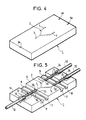
- FIG. 4 corresponds to a variant of the step given in FIG. 2.
- the waveguides 1 are produced in the central part of the substrate 1, in slightly overflowing on either side of them.
- Simple marks denoted 3A, 4A and 5A are produced at the same time as the waveguides and by the same integrated optical process, in the extension of the individual guides 3, 4, 5 in the vicinity of the edges of the substrate. Under these conditions, it is these marks and the ends of the waveguides which serve as a guide for tracing the grooves according to the step of FIG. 3.
- FIG 5 there is shown the integrated optical component of Figure 1 on which an optical fiber 30 is connected to the waveguide 3 and, similarly fibers 40 and 50 to the guides 4 and 5 and are all sealed to the substrate.
- These optical fibers are each covered with a resin coating 32 or 42 or 52.
- the end of each is prepared, by removing the coating as shown and specified below in look at the mounting of the fibers in the longitudinal grooves. Then, each fiber is placed on the substrate in its longitudinal grooves and is positioned substantially in contact with the end of the corresponding waveguide, against the connection interface shoulder.
- the part covered with the covering 32 is in the wide longitudinal groove 23, and its stripped end part 30 extends in the longitudinal groove 13, comes to bear on the rib 9, and comes at above the transverse groove 7 at the end of the waveguide 3.
- the fibers may not be stripped at the level of the retaining ribs and thus be sealed to the ribs.
Landscapes
- Physics & Mathematics (AREA)
- General Physics & Mathematics (AREA)
- Optics & Photonics (AREA)
- Optical Couplings Of Light Guides (AREA)
- Optical Integrated Circuits (AREA)
- Mechanical Coupling Of Light Guides (AREA)
Applications Claiming Priority (2)
| Application Number | Priority Date | Filing Date | Title |
|---|---|---|---|
| FR9005408A FR2661516B1 (fr) | 1990-04-27 | 1990-04-27 | Composant d'optique integree et procede de fabrication. |
| FR9005408 | 1990-04-27 |
Publications (2)
| Publication Number | Publication Date |
|---|---|
| EP0455090A1 true EP0455090A1 (de) | 1991-11-06 |
| EP0455090B1 EP0455090B1 (de) | 1995-02-15 |
Family
ID=9396177
Family Applications (1)
| Application Number | Title | Priority Date | Filing Date |
|---|---|---|---|
| EP91106456A Expired - Lifetime EP0455090B1 (de) | 1990-04-27 | 1991-04-22 | Integriert optische Komponente und Verfahren ihrer Herstellung |
Country Status (7)
| Country | Link |
|---|---|
| US (1) | US5123068A (de) |
| EP (1) | EP0455090B1 (de) |
| JP (1) | JPH06342113A (de) |
| CA (1) | CA2041236C (de) |
| DE (1) | DE69107326T2 (de) |
| FI (1) | FI911992A7 (de) |
| FR (1) | FR2661516B1 (de) |
Cited By (3)
| Publication number | Priority date | Publication date | Assignee | Title |
|---|---|---|---|---|
| EP0574734A1 (de) * | 1992-06-19 | 1993-12-22 | Corning Incorporated | Optisches Bauelement gekoppelt an eine lineare Anordnung von optischen Fasern |
| EP0603817A1 (de) * | 1992-12-23 | 1994-06-29 | Fraunhofer-Gesellschaft Zur Förderung Der Angewandten Forschung E.V. | Verfahren zum Verbinden von Lichtwellenleitern mit integriert optischen Bauelementen |
| FR2724057A1 (fr) * | 1994-08-26 | 1996-03-01 | Alcatel Nv | Procede de realisation d'un repere sur une plaquette notamment semiconductrice incluant une structure enterree |
Families Citing this family (24)
| Publication number | Priority date | Publication date | Assignee | Title |
|---|---|---|---|---|
| FR2674033B1 (fr) * | 1991-03-14 | 1993-07-23 | Corning Inc | Composant optique integre a liaison entre un guide d'onde integre et une fibre optique, fonctionnant dans un large domaine de temperature. |
| KR960014123B1 (ko) * | 1991-05-20 | 1996-10-14 | 후루카와덴기코교 카부시키가이샤 | 광도파로와 광파이버의 접속방법 |
| DE4130047A1 (de) * | 1991-09-10 | 1993-03-18 | Standard Elektrik Lorenz Ag | Verfahren zum betreiben eines halbleiterbauelements als optisches filter und halbleiterbauelement zur durchfuehrung des verfahrens |
| DE69131379T2 (de) * | 1991-11-25 | 2000-04-06 | Corning Inc. | Herstellungs- und Messmethode von integriert-optischen Komponenten |
| JPH05333231A (ja) * | 1992-05-29 | 1993-12-17 | Furukawa Electric Co Ltd:The | 光導波路と光ファイバの接続方法 |
| US5343544A (en) * | 1993-07-02 | 1994-08-30 | Minnesota Mining And Manufacturing Company | Integrated optical fiber coupler and method of making same |
| JP2550890B2 (ja) * | 1993-10-28 | 1996-11-06 | 日本電気株式会社 | 光導波路の接続構造およびその製造方法 |
| WO1996000996A1 (en) * | 1994-06-30 | 1996-01-11 | The Whitaker Corporation | Planar hybrid optical amplifier |
| US5907649A (en) * | 1994-09-26 | 1999-05-25 | Siemens Aktiengesellschaft | Coupling arrangement for optically coupling together an OEIC module and optical fibers |
| US5471552A (en) * | 1995-02-22 | 1995-11-28 | Industrial Technology Research Institute | Fabrication of static-alignment fiber-guiding grooves for planar lightwave circuits |
| JPH08286073A (ja) * | 1995-04-18 | 1996-11-01 | Sumitomo Electric Ind Ltd | 光導波路の実装用パッケージ構造 |
| JP3205227B2 (ja) * | 1995-08-16 | 2001-09-04 | アルプス電気株式会社 | 光導波素子及びその製造方法 |
| DE19619353A1 (de) * | 1996-05-14 | 1997-11-20 | Bosch Gmbh Robert | Verfahren zur Herstellung eines integriert optischen Wellenleiterbauteiles sowie Anordnung |
| KR100265789B1 (ko) * | 1997-07-03 | 2000-09-15 | 윤종용 | 광섬유수동정렬방법 |
| JPH11125731A (ja) * | 1997-10-22 | 1999-05-11 | Nec Corp | 単芯アレイ変換光装置 |
| GB2335756A (en) * | 1998-02-14 | 1999-09-29 | Integrated Optical Components | Connecting optic fibres to waveguides |
| JP3631622B2 (ja) * | 1998-09-29 | 2005-03-23 | 京セラ株式会社 | 光導波路と光ファイバとの接続構造および接続方法 |
| US6848839B2 (en) | 2000-04-07 | 2005-02-01 | Shipley Company, L.L.C. | Methods and devices for coupling optoelectronic packages |
| US6866426B1 (en) | 2000-04-07 | 2005-03-15 | Shipley Company, L.L.C. | Open face optical fiber array for coupling to integrated optic waveguides and optoelectronic submounts |
| US6788853B2 (en) * | 2000-06-28 | 2004-09-07 | Shipley Company, L.L.C. | Method for cleaving integrated optic waveguides to provide a smooth waveguide endface |
| US20050284181A1 (en) * | 2004-06-29 | 2005-12-29 | Smith Terry L | Method for making an optical waveguide assembly with integral alignment features |
| US9103987B2 (en) * | 2010-12-29 | 2015-08-11 | Alcatel Lucent | Optical amplifier for multi-core optical fiber |
| US11460637B2 (en) * | 2019-05-15 | 2022-10-04 | Corning Research & Development Corporation | Optical connection substrates for passive fiber to waveguide coupling |
| US10962726B2 (en) * | 2019-09-03 | 2021-03-30 | Lumentum Operations Llc | Structure for fiber attachment with adhesive material |
Citations (1)
| Publication number | Priority date | Publication date | Assignee | Title |
|---|---|---|---|---|
| EP0283203A1 (de) * | 1987-03-12 | 1988-09-21 | Corning Glass Works | Integrierter optischer Baustein und Methode zu seiner Herstellung |
Family Cites Families (3)
| Publication number | Priority date | Publication date | Assignee | Title |
|---|---|---|---|---|
| JPS60111203A (ja) * | 1983-11-18 | 1985-06-17 | Omron Tateisi Electronics Co | 光導波路装置 |
| JPS6155616A (ja) * | 1984-08-24 | 1986-03-20 | Shimadzu Corp | 光分流器の作成方法 |
| US4750800A (en) * | 1986-11-04 | 1988-06-14 | United Technologies Corporation | Low stress mounting of integrated optic chips |
-
1990
- 1990-04-27 FR FR9005408A patent/FR2661516B1/fr not_active Expired - Lifetime
-
1991
- 1991-04-22 EP EP91106456A patent/EP0455090B1/de not_active Expired - Lifetime
- 1991-04-22 US US07/688,236 patent/US5123068A/en not_active Expired - Fee Related
- 1991-04-22 DE DE69107326T patent/DE69107326T2/de not_active Expired - Fee Related
- 1991-04-24 FI FI911992A patent/FI911992A7/fi not_active Application Discontinuation
- 1991-04-25 CA CA002041236A patent/CA2041236C/fr not_active Expired - Fee Related
- 1991-04-26 JP JP3191342A patent/JPH06342113A/ja active Pending
Patent Citations (1)
| Publication number | Priority date | Publication date | Assignee | Title |
|---|---|---|---|---|
| EP0283203A1 (de) * | 1987-03-12 | 1988-09-21 | Corning Glass Works | Integrierter optischer Baustein und Methode zu seiner Herstellung |
Non-Patent Citations (3)
| Title |
|---|
| INTERNATIONAL CONFERENCE ON INTEGRATED OPTICS AND OPTICAL FIBRE COMMUNICATION, 11th EUROPEAN CONFERENCE ON OPTICAL COMMUNICATION, Venezia, 1-4 octobre 1985, pages 187-190; P. BARLIER et al.: "Passive integrated optics components for fiber optics communication in moldable glass" * |
| PATENT ABSTRACTS OF JAPAN, vol. 10, no. 215 (P-482)[2276], 31 juillet 1986; & JP-A-61 55 616 (SHIMADZU CORP.) 20-03-1986 * |
| PATENT ABSTRACTS OF JAPAN, vol. 9, no. 262 (P-398)[1985], 19 octobre 1985; & JP-A-60 111 203 (TATEISHI DENKI) 17-06-1985 * |
Cited By (7)
| Publication number | Priority date | Publication date | Assignee | Title |
|---|---|---|---|---|
| EP0574734A1 (de) * | 1992-06-19 | 1993-12-22 | Corning Incorporated | Optisches Bauelement gekoppelt an eine lineare Anordnung von optischen Fasern |
| FR2692684A1 (fr) * | 1992-06-19 | 1993-12-24 | Corning Inc | Composant optique connecté à un réseau de fibres optiques. |
| US5528713A (en) * | 1992-06-19 | 1996-06-18 | Corning Incorporated | Optical component connected to an array of optical fibers |
| EP0603817A1 (de) * | 1992-12-23 | 1994-06-29 | Fraunhofer-Gesellschaft Zur Förderung Der Angewandten Forschung E.V. | Verfahren zum Verbinden von Lichtwellenleitern mit integriert optischen Bauelementen |
| FR2724057A1 (fr) * | 1994-08-26 | 1996-03-01 | Alcatel Nv | Procede de realisation d'un repere sur une plaquette notamment semiconductrice incluant une structure enterree |
| EP0703616A1 (de) * | 1994-08-26 | 1996-03-27 | Alcatel N.V. | Verfahren zur Herstellung eines Markierungszeichens auf einer Halbleiterscheibe mit einer vergrabenen Struktur |
| US5616522A (en) * | 1994-08-26 | 1997-04-01 | Alcatel N.V. | Method of making a mark on a wafer such as a semiconductor wafer incorporating a buried structure |
Also Published As
| Publication number | Publication date |
|---|---|
| FI911992A0 (fi) | 1991-04-24 |
| CA2041236A1 (fr) | 1991-10-28 |
| FI911992L (fi) | 1991-10-28 |
| CA2041236C (fr) | 1996-03-19 |
| JPH06342113A (ja) | 1994-12-13 |
| DE69107326D1 (de) | 1995-03-23 |
| US5123068A (en) | 1992-06-16 |
| FR2661516B1 (fr) | 1992-06-12 |
| FR2661516A1 (fr) | 1991-10-31 |
| DE69107326T2 (de) | 1995-06-14 |
| EP0455090B1 (de) | 1995-02-15 |
| FI911992A7 (fi) | 1991-10-28 |
Similar Documents
| Publication | Publication Date | Title |
|---|---|---|
| EP0455090B1 (de) | Integriert optische Komponente und Verfahren ihrer Herstellung | |
| EP0670507B1 (de) | Verfahren zur Bildung einer optischen Mehrweg-Verbindungsanordnung, insbesondere für optische Fasern | |
| EP3715925B1 (de) | Chip für photonischen integrierten schaltkreis | |
| WO1991013378A1 (fr) | Procede de connexion entre une fibre optique et un microguide optique | |
| FR2545617A1 (fr) | Structure de support pour la fixation de fibres optiques et de lentilles et procede pour leur preparation ainsi que dispositif les utilisant | |
| FR2612301A1 (fr) | Composant optique integre et sa fabrication | |
| CA2087014A1 (en) | Method of connecting optical waveguide and optical fiber | |
| EP2216663B1 (de) | Struktur und Verfahren zur Justierung einer optischen Faser mit einem sub-mikronischen Lichtwellenleiter | |
| EP0729042B1 (de) | Segmentierter optischer Leiter, dessen Verwendung insbesondere in einer Halbleitervorrichtung | |
| EP0674197B1 (de) | Verfahren zur Herstellung eines Bauteils zum Anschluss an eine Mehrkernfaser | |
| FR2774180A1 (fr) | Procede passif de connectorisation d'elements optiques avec un circuit d'optique integree et gabarit pour la mise en oeuvre du procede | |
| EP2410361B1 (de) | Planarer, nanophotonischer Wellenleiter, der eine optische Kupplungsstruktur mit einer optischen Faser umfasst | |
| EP0456026A1 (de) | Optische Vorrichtung mit einem integriert optischen Element und Verfahren zu ihrer Herstellung | |
| CA2063208C (fr) | Procede de raccordement de deux cables a fibres optiques par epissurage | |
| EP0520952A1 (de) | Verfahren zum Koppeln einer optischen Faser an ein optoelektronisches Bauelement und so erhaltene Aufnahmevorrichtung | |
| FR2777662A1 (fr) | Procede d'assemblage d'un module optique | |
| EP1160602A1 (de) | Ausrichtung eines Flipchiplasers in einer schrägen Position auf einer Montageebene mit Ausrichtpfosten | |
| FR2661514A1 (fr) | Dispositif d'aboutage de fibres optiques sur un substrat d'optique integree. | |
| FR2830628A1 (fr) | Support de positionnement et de maintien de fibres optiques et procede de realisation d'un tel support | |
| CH639497A5 (fr) | Procede de realisation d'un coupleur directionnel de fibres optiques et jonction-etoile obtenue par ce procede. | |
| FR3071327B1 (fr) | Procede et systeme d'alignement de l'axe optique d'un cable optique avec un composant optoelectronique | |
| FR2661512A1 (fr) | Procede de connexion d'une fibre optique a un guide d'ondes d'optique integree et composant optique resultant. | |
| FR2744531A1 (fr) | Procede pour la realisation d'une structure comportant un guide optique et une cavite alignee avec precision sur ledit guide | |
| WO2002046798A2 (fr) | Structure de separation et de positionnement d'un de fibres optiques | |
| EP1386188A2 (de) | Halte- und indexationselement für eine asymetrische wellenleiterstruktur |
Legal Events
| Date | Code | Title | Description |
|---|---|---|---|
| PUAI | Public reference made under article 153(3) epc to a published international application that has entered the european phase |
Free format text: ORIGINAL CODE: 0009012 |
|
| AK | Designated contracting states |
Kind code of ref document: A1 Designated state(s): CH DE FR GB IT LI NL |
|
| 17P | Request for examination filed |
Effective date: 19920506 |
|
| 17Q | First examination report despatched |
Effective date: 19940527 |
|
| GRAA | (expected) grant |
Free format text: ORIGINAL CODE: 0009210 |
|
| AK | Designated contracting states |
Kind code of ref document: B1 Designated state(s): CH DE FR GB IT LI NL |
|
| PG25 | Lapsed in a contracting state [announced via postgrant information from national office to epo] |
Ref country code: NL Effective date: 19950215 |
|
| REF | Corresponds to: |
Ref document number: 69107326 Country of ref document: DE Date of ref document: 19950323 |
|
| ITF | It: translation for a ep patent filed | ||
| GBT | Gb: translation of ep patent filed (gb section 77(6)(a)/1977) |
Effective date: 19950421 |
|
| NLV1 | Nl: lapsed or annulled due to failure to fulfill the requirements of art. 29p and 29m of the patents act | ||
| PLBE | No opposition filed within time limit |
Free format text: ORIGINAL CODE: 0009261 |
|
| STAA | Information on the status of an ep patent application or granted ep patent |
Free format text: STATUS: NO OPPOSITION FILED WITHIN TIME LIMIT |
|
| 26N | No opposition filed | ||
| PGFP | Annual fee paid to national office [announced via postgrant information from national office to epo] |
Ref country code: GB Payment date: 20000313 Year of fee payment: 10 |
|
| PGFP | Annual fee paid to national office [announced via postgrant information from national office to epo] |
Ref country code: DE Payment date: 20000320 Year of fee payment: 10 |
|
| PGFP | Annual fee paid to national office [announced via postgrant information from national office to epo] |
Ref country code: CH Payment date: 20000323 Year of fee payment: 10 |
|
| PGFP | Annual fee paid to national office [announced via postgrant information from national office to epo] |
Ref country code: FR Payment date: 20000327 Year of fee payment: 10 |
|
| PG25 | Lapsed in a contracting state [announced via postgrant information from national office to epo] |
Ref country code: GB Free format text: LAPSE BECAUSE OF NON-PAYMENT OF DUE FEES Effective date: 20010422 |
|
| PG25 | Lapsed in a contracting state [announced via postgrant information from national office to epo] |
Ref country code: FR Free format text: THE PATENT HAS BEEN ANNULLED BY A DECISION OF A NATIONAL AUTHORITY Effective date: 20010430 |
|
| PG25 | Lapsed in a contracting state [announced via postgrant information from national office to epo] |
Ref country code: LI Free format text: LAPSE BECAUSE OF NON-PAYMENT OF DUE FEES Effective date: 20010521 Ref country code: CH Free format text: LAPSE BECAUSE OF NON-PAYMENT OF DUE FEES Effective date: 20010521 |
|
| GBPC | Gb: european patent ceased through non-payment of renewal fee |
Effective date: 20010422 |
|
| REG | Reference to a national code |
Ref country code: CH Ref legal event code: PL |
|
| PG25 | Lapsed in a contracting state [announced via postgrant information from national office to epo] |
Ref country code: DE Free format text: LAPSE BECAUSE OF NON-PAYMENT OF DUE FEES Effective date: 20020201 |
|
| REG | Reference to a national code |
Ref country code: FR Ref legal event code: ST |
|
| PG25 | Lapsed in a contracting state [announced via postgrant information from national office to epo] |
Ref country code: IT Free format text: LAPSE BECAUSE OF NON-PAYMENT OF DUE FEES;WARNING: LAPSES OF ITALIAN PATENTS WITH EFFECTIVE DATE BEFORE 2007 MAY HAVE OCCURRED AT ANY TIME BEFORE 2007. THE CORRECT EFFECTIVE DATE MAY BE DIFFERENT FROM THE ONE RECORDED. Effective date: 20050422 |