EP0455325A1 - Monocristaux de phosphure d'indium semi-isolants et méthode pour leur préparation - Google Patents
Monocristaux de phosphure d'indium semi-isolants et méthode pour leur préparation Download PDFInfo
- Publication number
- EP0455325A1 EP0455325A1 EP91301722A EP91301722A EP0455325A1 EP 0455325 A1 EP0455325 A1 EP 0455325A1 EP 91301722 A EP91301722 A EP 91301722A EP 91301722 A EP91301722 A EP 91301722A EP 0455325 A1 EP0455325 A1 EP 0455325A1
- Authority
- EP
- European Patent Office
- Prior art keywords
- single crystal
- inp single
- inp
- semi
- concentration
- Prior art date
- Legal status (The legal status is an assumption and is not a legal conclusion. Google has not performed a legal analysis and makes no representation as to the accuracy of the status listed.)
- Granted
Links
Images




Classifications
-
- C—CHEMISTRY; METALLURGY
- C30—CRYSTAL GROWTH
- C30B—SINGLE-CRYSTAL GROWTH; UNIDIRECTIONAL SOLIDIFICATION OF EUTECTIC MATERIAL OR UNIDIRECTIONAL DEMIXING OF EUTECTOID MATERIAL; REFINING BY ZONE-MELTING OF MATERIAL; PRODUCTION OF A HOMOGENEOUS POLYCRYSTALLINE MATERIAL WITH DEFINED STRUCTURE; SINGLE CRYSTALS OR HOMOGENEOUS POLYCRYSTALLINE MATERIAL WITH DEFINED STRUCTURE; AFTER-TREATMENT OF SINGLE CRYSTALS OR A HOMOGENEOUS POLYCRYSTALLINE MATERIAL WITH DEFINED STRUCTURE; APPARATUS THEREFOR
- C30B33/00—After-treatment of single crystals or homogeneous polycrystalline material with defined structure
-
- C—CHEMISTRY; METALLURGY
- C30—CRYSTAL GROWTH
- C30B—SINGLE-CRYSTAL GROWTH; UNIDIRECTIONAL SOLIDIFICATION OF EUTECTIC MATERIAL OR UNIDIRECTIONAL DEMIXING OF EUTECTOID MATERIAL; REFINING BY ZONE-MELTING OF MATERIAL; PRODUCTION OF A HOMOGENEOUS POLYCRYSTALLINE MATERIAL WITH DEFINED STRUCTURE; SINGLE CRYSTALS OR HOMOGENEOUS POLYCRYSTALLINE MATERIAL WITH DEFINED STRUCTURE; AFTER-TREATMENT OF SINGLE CRYSTALS OR A HOMOGENEOUS POLYCRYSTALLINE MATERIAL WITH DEFINED STRUCTURE; APPARATUS THEREFOR
- C30B29/00—Single crystals or homogeneous polycrystalline material with defined structure characterised by the material or by their shape
- C30B29/10—Inorganic compounds or compositions
- C30B29/40—AIIIBV compounds wherein A is B, Al, Ga, In or Tl and B is N, P, As, Sb or Bi
-
- H—ELECTRICITY
- H10—SEMICONDUCTOR DEVICES; ELECTRIC SOLID-STATE DEVICES NOT OTHERWISE PROVIDED FOR
- H10D—INORGANIC ELECTRIC SEMICONDUCTOR DEVICES
- H10D30/00—Field-effect transistors [FET]
- H10D30/60—Insulated-gate field-effect transistors [IGFET]
-
- H—ELECTRICITY
- H10—SEMICONDUCTOR DEVICES; ELECTRIC SOLID-STATE DEVICES NOT OTHERWISE PROVIDED FOR
- H10D—INORGANIC ELECTRIC SEMICONDUCTOR DEVICES
- H10D62/00—Semiconductor bodies, or regions thereof, of devices having potential barriers
- H10D62/80—Semiconductor bodies, or regions thereof, of devices having potential barriers characterised by the materials
- H10D62/85—Semiconductor bodies, or regions thereof, of devices having potential barriers characterised by the materials being Group III-V materials, e.g. GaAs
- H10D62/854—Semiconductor bodies, or regions thereof, of devices having potential barriers characterised by the materials being Group III-V materials, e.g. GaAs further characterised by the dopants
Definitions
- the amount of Fe, Co or Cr doping the compound semiconductor crystals for the semi-insulation is preferred to be as small as possible. This is because Fe, Co and Cr serve as deep acceptors, an ion implanted electronic devices an substrates made of these Fe, Co or Cr doped compound semiconductor crystals, e.g., an FET, and they reduce the activation efficiency of implanted ions in. In the case of devices operating at high frequencies such as an OEIC or HEMT, Fe, Co and Cr diffuse in the epitaxial layers, trap carriers and deteriorate high-frequency and high-speed performances.
- a reduced concentration of all of Fe, Co and Cr in the compound semiconductor single crystal reduces the resistivity of the compound semiconductor single crystal since the concentration of a native impurity (i.e., residual impurity) providing a donor amounts to a level of reduced concentration of all of the Fe, Co and Cr.
- a native impurity i.e., residual impurity
- the present inventors proposed that the electrically active point defect, as well as the compensation by donors and deep acceptors characterize the mechanism of semi-insulating the InP single crystal and diligently studied to discover that controlling the density of the point defect by means of heat-treating the InP single crystal caused even a much lower concentration of the deep acceptors than a prior art concentration thereof so as to semi-insulate the InP single crystal or compound semiconductor single crystal.
- the present inventors further studied from the process of the Japanese patent application SHO. 63-220632 to discover that even heat-treating an undoped InP single crystal including a concentration of 0.05 ppmw or less for all of Fe, Co and Cr failed to semi-insulate the crystal.
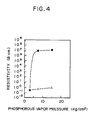
- heat-treating the InP single crystal wafer produced from the raw InP polycrystal of the 5 ⁇ 1015 cm ⁇ 3 carrier concentration under the absolute phosphorous vapor pressure of 7.5 kg/cm2 failed to provide an InP single crystal wafer of a high resistivity and on the other hand, heat-treating the InP single crystal wafer produced from the raw InP polycrystal having the 5 ⁇ 1014 cm ⁇ 3 carrier concentration under absolute the phosphorous vapor pressure of 6 kg/cm2 failed to provide an InP single crystal wafer of a high resistivity.
- the resistivities of the both were 4,000 cm2/V ⁇ s or more.
- a carrier concentration of 3 ⁇ 1015 cm ⁇ 3 or less of the raw InP polycrystal provides a resistivity of 106 ⁇ cm or more for the final InP single crystal wafer and a mobility of 300 cm2/V ⁇ s or more.
- the mobility of the final InP single crystal wafer increases beyond a carrier concentration of 5 ⁇ 1015 cm ⁇ 3 because the final InP single crystal wafer was not semi-insulating.
- Examples 1-3 have described the InP single crystal wafer when the heat treatment temperature was 900 °C. However, a semi-insulating InP single crystal, semiconductor device with a substrate of crystal and processes of producing them are disclosed. Heat-treating an undoped InP single crystal having a concentration of 0.05 ppmw or less for all native Fe, Co and Cr under a phosphorous vapor pressure at other temperatures provided a semi-insulating InP single crystal of a resistivity of 1 ⁇ 106 ⁇ cm or more and a mobility of above 3,000 cm2/V ⁇ s both at 300 K.
- Example 4 describes a MISFET with a substrate made of an InP single crystal wafer of the first aspect of the present invention and a process for producing the MISFET.
- An undoped n-type InP single crystal ingot with a 2-inch diameter and a concentration of 0.05 ppmw or less for all of Fe, Co and Cr was grown along the ⁇ 100> orientation from a raw InP polycrystal having a carrier concentration of 1 ⁇ 1015 cm ⁇ 3 by the Liquid encapsulated Czochralski method.
- the InP single crystal ingot was sliced in a transverse direction to the pull axis thereof.
- the sliced InP wafer was washed with an organic solvent, then etched with bromomethanol and then washed with HF (i.e., hydrofluoric acid) immediately before an oxidation of the InP wafer.
- HF i.e., hydrofluoric acid
- the InP wafer and red phosphorous were placed in a quartz ampoule.
- a gas in the quartz ampoule was evacuated so that the pressure therein was 1 ⁇ 10 ⁇ 6 torr.
- an oxyhydrogen burner melted the open end of the quartz ampoule to seal the quartz ampoule.
- the amount of the red phosphorous was adjusted so that the phosphorous vapor absolute pressure in the quartz ampoule was 15 kg/cm2 at 900 °C, i.e., a heat-treatment temperature. Then, the quartz ampoule was placed in the horizontal heating furnace, heated and held at a 900 °C for 20 hr and then naturally cooled.
- a 50 ⁇ m square part of the surface of each of InP wafers of Example 4 was lapped. Then, the resistivity and mobility of the InP wafer were measured at 300 K by Van Der Pauw method.
- the resistivity of the InP single crystal wafer was 1.5 ⁇ 107 ⁇ cm or more.
- the mobility thereof was 4,400 cm2/V ⁇ s.
- the semi-insulating InP single crystal wafer was pretreated with a phosphoric acid etchant. Then, the pretreated InP single crystal wafer and a predetermined amount of phosphorus were placed in a quartz ampoule. A gas in the quartz ampoule was evacuated to vacuum. Then, oxygen gas of a pressure of 1.0 atm was introduced into the quartz ampoule. Then, the quartz ampoule was sealed. The predetermined amount of phosphorus was such that the phosphorous vapor pressure was a pressure of 0.9 atm in a heating of the quartz ampoule. Then, the quartz ampoule was heated at 500 °C for 5 hr, which produced a thermal oxidation film on the surface of the InP single crystal. Then, the quartz ampoule was cooled and then opened. Measuring the thickness of the thermal oxidation film provided about 40 nm.
- n+-contact layers 2a and 2b providing a source domain and a drain domain in an upper area of the InP single crystal wafer.
- a spacing between the n+-contact layers 2a and 2b was 1 ⁇ m.
- Example 4 employed the thermal oxidation film as the gate insulation film.
- an SiN x film or SiO2 film produced by sputtering, plasma-enhanced CVD or the like may be employed.
- Example 4 produced the n+-contact layers after a production of the gate insulation film. However, alternatively the n+-contact layers and the gate insulation film may be sequentially produced.
Landscapes
- Chemical & Material Sciences (AREA)
- Engineering & Computer Science (AREA)
- Crystallography & Structural Chemistry (AREA)
- Materials Engineering (AREA)
- Metallurgy (AREA)
- Organic Chemistry (AREA)
- Inorganic Chemistry (AREA)
- Crystals, And After-Treatments Of Crystals (AREA)
Applications Claiming Priority (6)
| Application Number | Priority Date | Filing Date | Title |
|---|---|---|---|
| JP5137090 | 1990-03-02 | ||
| JP51370/90 | 1990-03-02 | ||
| JP2115403A JP2572291B2 (ja) | 1990-03-02 | 1990-05-01 | 半絶縁性InP単結晶基板の製造方法 |
| JP115403/90 | 1990-05-01 | ||
| JP122669/90 | 1990-05-11 | ||
| JP12266990A JPH0418761A (ja) | 1990-05-11 | 1990-05-11 | 化合物半導体装置およびその製造方法 |
Publications (2)
| Publication Number | Publication Date |
|---|---|
| EP0455325A1 true EP0455325A1 (fr) | 1991-11-06 |
| EP0455325B1 EP0455325B1 (fr) | 1994-08-17 |
Family
ID=27294293
Family Applications (1)
| Application Number | Title | Priority Date | Filing Date |
|---|---|---|---|
| EP91301722A Expired - Lifetime EP0455325B1 (fr) | 1990-03-02 | 1991-03-01 | Monocristaux de phosphure d'indium semi-isolants et méthode pour leur préparation |
Country Status (3)
| Country | Link |
|---|---|
| US (1) | US5173127A (fr) |
| EP (1) | EP0455325B1 (fr) |
| DE (1) | DE69103464T2 (fr) |
Cited By (1)
| Publication number | Priority date | Publication date | Assignee | Title |
|---|---|---|---|---|
| CN103361735A (zh) * | 2012-03-26 | 2013-10-23 | 北京通美晶体技术有限公司 | 一种iiia-va族半导体单晶衬底及其制备方法 |
Families Citing this family (4)
| Publication number | Priority date | Publication date | Assignee | Title |
|---|---|---|---|---|
| US5314547A (en) * | 1992-09-28 | 1994-05-24 | General Motors Corporation | Rare earth slab doping of group III-V compounds |
| JPH08236442A (ja) * | 1995-02-28 | 1996-09-13 | Mitsubishi Electric Corp | 半導体ウエハ,及びその製造方法 |
| US6749691B2 (en) * | 2001-02-14 | 2004-06-15 | Air Liquide America, L.P. | Methods of cleaning discolored metallic arrays using chemical compositions |
| US20050059260A1 (en) * | 2003-09-15 | 2005-03-17 | Haowen Bu | CMOS transistors and methods of forming same |
Citations (2)
| Publication number | Priority date | Publication date | Assignee | Title |
|---|---|---|---|---|
| DE2544286A1 (de) * | 1974-10-07 | 1976-04-08 | Mitsubishi Electric Corp | Verfahren zum zuechten halbisolierender halbleiterkristalle aus verbindungen iii bis v |
| EP0196854A2 (fr) * | 1985-03-28 | 1986-10-08 | Kabushiki Kaisha Toshiba | Méthode de synthèse d'un composé de phosphore et d'un élément du groupe III |
Family Cites Families (2)
| Publication number | Priority date | Publication date | Assignee | Title |
|---|---|---|---|---|
| US4268844A (en) * | 1979-12-31 | 1981-05-19 | The United States Of America As Represented By The Secretary Of The Navy | Insulated gate field-effect transistors |
| JPS63220632A (ja) * | 1987-03-10 | 1988-09-13 | Sony Corp | 情報伝送装置 |
-
1991
- 1991-02-28 US US07/661,616 patent/US5173127A/en not_active Expired - Fee Related
- 1991-03-01 EP EP91301722A patent/EP0455325B1/fr not_active Expired - Lifetime
- 1991-03-01 DE DE69103464T patent/DE69103464T2/de not_active Expired - Fee Related
Patent Citations (2)
| Publication number | Priority date | Publication date | Assignee | Title |
|---|---|---|---|---|
| DE2544286A1 (de) * | 1974-10-07 | 1976-04-08 | Mitsubishi Electric Corp | Verfahren zum zuechten halbisolierender halbleiterkristalle aus verbindungen iii bis v |
| EP0196854A2 (fr) * | 1985-03-28 | 1986-10-08 | Kabushiki Kaisha Toshiba | Méthode de synthèse d'un composé de phosphore et d'un élément du groupe III |
Non-Patent Citations (1)
| Title |
|---|
| APPLIED PHYSICS, vol. A48, 1989, pages 315-319, New York, US; D. HOFMANN et al.: "Semi-insulating electrical properties of undoped InP after heat treatment in a phosphorus atmosphere" * |
Cited By (1)
| Publication number | Priority date | Publication date | Assignee | Title |
|---|---|---|---|---|
| CN103361735A (zh) * | 2012-03-26 | 2013-10-23 | 北京通美晶体技术有限公司 | 一种iiia-va族半导体单晶衬底及其制备方法 |
Also Published As
| Publication number | Publication date |
|---|---|
| DE69103464T2 (de) | 1994-12-15 |
| DE69103464D1 (de) | 1994-09-22 |
| US5173127A (en) | 1992-12-22 |
| EP0455325B1 (fr) | 1994-08-17 |
Similar Documents
| Publication | Publication Date | Title |
|---|---|---|
| Ta et al. | Effects of stoichiometry on thermal stability of undoped, semi‐insulating GaAs | |
| US4784975A (en) | Post-oxidation anneal of silicon dioxide | |
| Kainosho et al. | Undoped semi‐insulating InP by high‐pressure annealing | |
| US3696276A (en) | Insulated gate field-effect device and method of fabrication | |
| JP2967780B1 (ja) | GaAs単結晶基板およびそれを用いたエピタキシャルウェハ | |
| US6056817A (en) | Process for producing semi-insulating InP single crystal and semi-insulating InP single crystal substrate | |
| US3994755A (en) | Liquid phase epitaxial process for growing semi-insulating GaAs layers | |
| EP0455325B1 (fr) | Monocristaux de phosphure d'indium semi-isolants et méthode pour leur préparation | |
| US5254507A (en) | Semi-insulating InP single crystals, semiconductor devices having substrates of the crystals and processes for producing the same | |
| US4028147A (en) | Liquid phase epitaxial process for growing semi-insulating GaAs layers | |
| JPH0750692B2 (ja) | ▲iii▼―▲v▼族化合物半導体の熱処理方法 | |
| US4032950A (en) | Liquid phase epitaxial process for growing semi-insulating gaas layers | |
| Otsubo et al. | Liquid Phase Epitaxial Growth of GaAs Crystals under a Mixed Gas Atmosphere | |
| JP2819244B2 (ja) | 半絶縁性InP単結晶の製造方法 | |
| JP2572291B2 (ja) | 半絶縁性InP単結晶基板の製造方法 | |
| JP3793934B2 (ja) | 半絶縁性InP単結晶の製造方法 | |
| JPS63119268A (ja) | 半導体装置の製造方法 | |
| JPH0632699A (ja) | 半絶縁性InP単結晶の製造方法 | |
| Falckenberg | Flame fusion growth of spinel and sapphire crystals for ESFI SOS technology | |
| Kitagawara et al. | Deep levels in semiconducting In‐alloyed bulk n‐GaAs and its resistivity conversions by thermal treatments | |
| JP2829403B2 (ja) | 化合物半導体の製造方法 | |
| JPH06295863A (ja) | 高抵抗化合物半導体の製造方法 | |
| JPH0492899A (ja) | 半絶縁性InP単結晶基板の製造方法 | |
| Imaizumi et al. | Semi‐insulation of undoped GaAs epitaxial layers by wafer annealing | |
| Uchida | Semi‐Insulating Behavior of InP Wafers Prepared by Phosphorus Vapor Pressure Controlled Wafer Annealing |
Legal Events
| Date | Code | Title | Description |
|---|---|---|---|
| PUAI | Public reference made under article 153(3) epc to a published international application that has entered the european phase |
Free format text: ORIGINAL CODE: 0009012 |
|
| AK | Designated contracting states |
Kind code of ref document: A1 Designated state(s): DE FR GB |
|
| 17P | Request for examination filed |
Effective date: 19920416 |
|
| 17Q | First examination report despatched |
Effective date: 19931028 |
|
| RAP1 | Party data changed (applicant data changed or rights of an application transferred) |
Owner name: JAPAN ENERGY CORPORATION |
|
| GRAA | (expected) grant |
Free format text: ORIGINAL CODE: 0009210 |
|
| AK | Designated contracting states |
Kind code of ref document: B1 Designated state(s): DE FR GB |
|
| REF | Corresponds to: |
Ref document number: 69103464 Country of ref document: DE Date of ref document: 19940922 |
|
| ET | Fr: translation filed | ||
| PLBE | No opposition filed within time limit |
Free format text: ORIGINAL CODE: 0009261 |
|
| STAA | Information on the status of an ep patent application or granted ep patent |
Free format text: STATUS: NO OPPOSITION FILED WITHIN TIME LIMIT |
|
| 26N | No opposition filed | ||
| PGFP | Annual fee paid to national office [announced via postgrant information from national office to epo] |
Ref country code: DE Payment date: 20000228 Year of fee payment: 10 |
|
| PGFP | Annual fee paid to national office [announced via postgrant information from national office to epo] |
Ref country code: GB Payment date: 20000301 Year of fee payment: 10 |
|
| PGFP | Annual fee paid to national office [announced via postgrant information from national office to epo] |
Ref country code: FR Payment date: 20000310 Year of fee payment: 10 |
|
| PG25 | Lapsed in a contracting state [announced via postgrant information from national office to epo] |
Ref country code: GB Free format text: LAPSE BECAUSE OF NON-PAYMENT OF DUE FEES Effective date: 20010301 |
|
| GBPC | Gb: european patent ceased through non-payment of renewal fee |
Effective date: 20010301 |
|
| PG25 | Lapsed in a contracting state [announced via postgrant information from national office to epo] |
Ref country code: FR Free format text: LAPSE BECAUSE OF NON-PAYMENT OF DUE FEES Effective date: 20011130 |
|
| REG | Reference to a national code |
Ref country code: FR Ref legal event code: ST |
|
| PG25 | Lapsed in a contracting state [announced via postgrant information from national office to epo] |
Ref country code: DE Free format text: LAPSE BECAUSE OF NON-PAYMENT OF DUE FEES Effective date: 20020101 |