EP0196854A2 - Méthode de synthèse d'un composé de phosphore et d'un élément du groupe III - Google Patents
Méthode de synthèse d'un composé de phosphore et d'un élément du groupe III Download PDFInfo
- Publication number
- EP0196854A2 EP0196854A2 EP86302170A EP86302170A EP0196854A2 EP 0196854 A2 EP0196854 A2 EP 0196854A2 EP 86302170 A EP86302170 A EP 86302170A EP 86302170 A EP86302170 A EP 86302170A EP 0196854 A2 EP0196854 A2 EP 0196854A2
- Authority
- EP
- European Patent Office
- Prior art keywords
- phosphorus
- group iii
- iii element
- compound
- pressure
- Prior art date
- Legal status (The legal status is an assumption and is not a legal conclusion. Google has not performed a legal analysis and makes no representation as to the accuracy of the status listed.)
- Granted
Links
Images


Classifications
-
- C—CHEMISTRY; METALLURGY
- C30—CRYSTAL GROWTH
- C30B—SINGLE-CRYSTAL GROWTH; UNIDIRECTIONAL SOLIDIFICATION OF EUTECTIC MATERIAL OR UNIDIRECTIONAL DEMIXING OF EUTECTOID MATERIAL; REFINING BY ZONE-MELTING OF MATERIAL; PRODUCTION OF A HOMOGENEOUS POLYCRYSTALLINE MATERIAL WITH DEFINED STRUCTURE; SINGLE CRYSTALS OR HOMOGENEOUS POLYCRYSTALLINE MATERIAL WITH DEFINED STRUCTURE; AFTER-TREATMENT OF SINGLE CRYSTALS OR A HOMOGENEOUS POLYCRYSTALLINE MATERIAL WITH DEFINED STRUCTURE; APPARATUS THEREFOR
- C30B15/00—Single-crystal growth by pulling from a melt, e.g. Czochralski method
-
- C—CHEMISTRY; METALLURGY
- C01—INORGANIC CHEMISTRY
- C01B—NON-METALLIC ELEMENTS; COMPOUNDS THEREOF; METALLOIDS OR COMPOUNDS THEREOF NOT COVERED BY SUBCLASS C01C
- C01B25/00—Phosphorus; Compounds thereof
- C01B25/08—Other phosphides
- C01B25/082—Other phosphides of boron, aluminium, gallium or indium
- C01B25/087—Other phosphides of boron, aluminium, gallium or indium of gallium or indium
-
- C—CHEMISTRY; METALLURGY
- C30—CRYSTAL GROWTH
- C30B—SINGLE-CRYSTAL GROWTH; UNIDIRECTIONAL SOLIDIFICATION OF EUTECTIC MATERIAL OR UNIDIRECTIONAL DEMIXING OF EUTECTOID MATERIAL; REFINING BY ZONE-MELTING OF MATERIAL; PRODUCTION OF A HOMOGENEOUS POLYCRYSTALLINE MATERIAL WITH DEFINED STRUCTURE; SINGLE CRYSTALS OR HOMOGENEOUS POLYCRYSTALLINE MATERIAL WITH DEFINED STRUCTURE; AFTER-TREATMENT OF SINGLE CRYSTALS OR A HOMOGENEOUS POLYCRYSTALLINE MATERIAL WITH DEFINED STRUCTURE; APPARATUS THEREFOR
- C30B29/00—Single crystals or homogeneous polycrystalline material with defined structure characterised by the material or by their shape
- C30B29/10—Inorganic compounds or compositions
- C30B29/40—AIIIBV compounds wherein A is B, Al, Ga, In or Tl and B is N, P, As, Sb or Bi
Definitions
- the present invention relates to a method of synthesizing a phosphorus compound which is used as a raw material in a pull-up production of monocrystal compound semiconductor, etc., and more particularly to a method of synthesizing Group III element-phosphorus monocrystal compounds in which a Group III element and phosphorus are directly synthesized together.
- GaP monocrystal is a semiconductor having a relatively large energy gap among others of the Group III-V compound semiconductor, and allows an easy control of the n and p conductive type control is relatively simple, and is therefore used as a raw material of light emitting diodes.
- the production of GaP offers various problems in synthesis, and therefore the production of GaP monocrystal has been extremely difficult. That is, phosphide has a high melting temperature, as is well known, and more over it exhibits a high decomposition pressure at that melting temperature. Accordingly, in the conventional method, phosphorus is vaporized so that the compound thereof decomposes causing it difficult to produce GaP monocrystal.
- a method generally known as "a high pressure pull-up method under a liquid encapsulate" has become applicable in the industrial production of monocrystal of phosphide such as, for example, GaP, etc..
- the top of GaP polycrystal which has been synthesized beforehand and received in a crusible is covered with B 2 0 3 having a low vapor pressure, and is then pressurized with the use of inert gas within the high pressure container. Under this condition the cruisable is heated to melt GaP.
- B 2 0 3 covers the top surface of GaP to prevent phosphorus from vaporizing.
- GaP monocrystal is pulled up through B203 (an encapsulate) to allow the growth of GaP monocrystals.
- the GaP polycrystal should be preliminarily synthesized by other means. Accordingly, in order to manufacture a high quality GaP monocrystal at a low cost, it is necessary to prepare a high quality GaP polycrystal at a low cost.
- the gas of H 2 + PH 3 is allowed to flow over Ga in a boat disposed within a heating furnace while Ga is heated up to a temperature of about 1000°C.
- GaP then is gradually synthesized from one end of the boat by inducing a temperature difference of 100°C between both ends of the boat.
- GaPO is fired and reduced in a hydrogen atmosphere at a temperature of 850°C.
- GaP polycrystals obtained by these methods are powder-like, so that the GaP polycrystals thus obtained should be further processed into a high-density before they are pull up to form a monocrystal thereof, resulting in that the steps are complicated and the price of the product increases.
- both low and high pressure synthesis methods mentioned above require a long time (several days) for the synthesis of GaP polycrystal, and therefore, not only incurs low productivity and an increase in cost but also presents the problem of contamination in a reaction system since the reaction system must be maintained at a high temperature for a long time.
- One object of the present invention is to provide a method of synthesizing a compound of Group III element and phosphorus in which a highly- dense polycrystal composed of the compounds of Group III elements and phosphorus can be produced with a high degree of efficiency in a short time, the introduction of impurities from a reaction system can also be reduced, and the production cost of the compound can be reduced.
- the present invention provides a method of synthesizing a Group III element-phosphorus compound, which comprises the steps of disposing a mixture of a Group III element and phosphorus in a pressurized inert gas atmosphere; and subjecting the mixture of the Group III element and phosphorus to a liquid-phase reaction under a heated and pressurized condition, thereby forming a polycrystal compound of a Group III element and phosphorus.
- the present invention is to provide a method of synthesizing a Group III element-phosphorus compound, which comprises the steps of disposing a mixture of a Group III element and phosphorus in a pressurized inert gas atmosphere; subjecting the mixture of the Group III element and phosphorus to a liquid-phase reaction under a heated and pressurized condition, thereby forming a compound of a Group III elements and phosphorus; and pulling up with a use of a seed crystal a Group III element-phosphorus compound monocrystal under such conditions that the top surface of the Group III element-phosphorus compound is covered with an encapsulating layer.
- the gist of the present invention is in that a Group III element and phosphorus are subjected to a liquid-phase reaction for direct synthesis.
- Red phosphorus normally exists as two allotropes of yellow phosphorus and red phosphorus under normal temperature and pressure.
- Red phosphorus has a stable phase in comparison with yellow phosphorus having its melting point around 44°C, and spontaneously ignites in the air.
- Yellow phosphorus, or liquid phosphorus has a metastable phase, and therefore, when its temperature reaches a temperature of around 250°C or when ultraviolet ray is irradiated, it is converted into red phosphorus and is solidified. On the contrary, when the mentioned above conditions are avoided, yellow phosphorus and liquid phosphorus remain in their stable conditions for a long time.
- Fig. 3 is a phase diagram of phosphorus on which the relationship among red phosphorus, yellow phosphorus and liquid phosphorus is shown.
- the curve 31 of A-B is the curve of vapor-pressure of red phosphorus, in which it is found that red phosphorus has a stable phase at a pressure less than about 43 atm. and at a temperature of less than 590°C.
- the line 32 of G-A which is a vapor-pressure curve of the liquid phase-gas phase, there exists the phase of metastable liquid phosphorus, and in the areas having a temperature lower than that, there exists the phase 33 of yellow phosphorus having a solid phase.
- the temperature of the solid phase yellow phosphorus is raised at normal pressure, it melts at a temperature of about 44°C and is changed into its liquid state. In this condition it is comparatively stable in the form of liquid phosphorus, but as the temperature gradually rises up to above 250°C, liquid phosphorus abruptly changes into red phosphorus.
- this liquid phosphorus is subjected to a liquid-phase reaction by externally heating a Group III element such as, for example, Ga, while the liquid phosphorus is maintained in a stable condition under a high pressure.
- a Group III element such as, for example, Ga
- the temperature thereof can be locally raised without requiring a large amount of external heating to a temperature near the melting point of phosphide to greatly promote the reaction of the Group III element and phosphorus. It is thereby possible to instantly complete the synthesis of the polycrystal compound.
- any inert gas other than N 2 gas may be used.
- an l inert gas such as, for example, Ar gas, which incurs high frequency electric discharge, is not preferable.
- N 2 gas is the most preferable.
- the pressure and heating temperature of the inert gas atmosphere should be set in a range of 130 to 700 atm. and in a range of 600 to 1450°C for the reaction.
- the optimum pressure and temperature can be suitably set in accordance with the kind of Group III elements to be used.
- the pressure of the inert gas should be set within a range of 300 to 700 atm, and the temperature within a range of 700 to 1450°C, more preferably 1300 to 1450 0 C .
- the pressure of the inert gas is preferably set within a range of 130 to 600 atm., more preferably 150 to 200 atm, and the temperature within a range of 600 to 1200°C, more preferably 1100 to 1200°C.
- phosphorus compound polycrystal (Group III-V compound semiconductor) having a high purity can be synthesized directly from a high purity Group III element and phosphorus. It is therefore possible to obtain high-density polycrystal suitable for pulling up Group III-V monocrystal semiconductor, in conformity with the shape of a crusible used for pulling up monocrystal. Further, the Group III element-phosphorus compound produces within the crusible, according to the method of the present invention, can be directly pulled up from the crusible with the use of a seed crystal, and the Group III element-phosphorus compound can be obtained as a monocrystal.
- the process of the synthesis is simple and therefore, can be completed in a short time, a large amount of phosphorus compound polycrystal or monocrystal can be produced at low cost thereby making the present invention a great contribution to the industries.
- Fig. 1 is a cross-sectional view which schematically shows the arrangement of a GaP polycrystal synthesizing device used in one embodiment of the invention.
- reference numeral 11 denotes a high pressure chamber composed of chamber members lla, llb made of stainless steel and charged therein with molybdenum.
- the chamber members lla, llb are fastened together with screws, etc.
- the chamber 11 is surrounded by a cooling pipe 12 laid along the peripheral surface thereof.
- a crusible 13 in which raw materials 21, 22 and an encapsulating material 23 are stored as explained hereinbelow.
- the crusible 13 is supported by a suscepter 14 around which a high frequency heating coil 15 is arranged. Further, the heating coil 15 is surrounded by a heat-insulating plate 16.
- reference numeral 17 denotes a gas introduction port through which inert gas such as N 2 gas is introduced.
- 18a, 18b denote electrodes for feeding the current to the coil 15, and 19a; 19b is the pressurizing mechanisms for preventing the chambers 11 from exploding.
- a high purity N 2 gas was introduced and compressed with about 250 atm. in the chamber 11 with the use of a pressurizing unit. Thereafter, with the use of the high frequency coil 15 (power source frequency of 500Hz), the crucible 15 was heated.
- the high frequency coil 15 power source frequency of 500Hz
- Fig. 2 shows one example of the heating patterns together with one example of the pressure patterns.
- the raw material 21, 22 and the encapsulating material 23 within the crucible 13 were gradually heated (in area a), and then the power for heating was temporarily held at the temperature at which B 2 0 3 soften so as to cover the raw material (in area b). Further, after B-0, was conditioned to sufficiently suppress the evaporation of phosphorus, synthesis was rapidly carried out (in the area c). Thereafter, heating was continued until synthe- l3s was completed (in the area d: the pressure in this stage was 480 atm.). Upon completion of synthesis, the heating of the raw materials was stopped and the resultant product was rapidly cooled (in the area f). In simultaneous with the cooling process, the internal pressure of the chamber was increased up to 540 atm. in order to prevent phosphorus from excessively scattering upon solidification of the molten liquid.
- composition ratio of Ga and P can be controlled.
- the inventors have tried to obtain a charge ratio which is optimum for a light-emitting diode substrate.
- the diffusion of boron from B 2 0 3 into the product in the condition A was larger than the condition B while the diffusion of impurities from the crucible material in the condition A was larger than the condition B. That is, polycrystal of higher purity can be obtained under the condition of excessiveness of P.
- monocrystal of high quality having for less amount of precipitation and voids can be obtained with the use of the polycrystal line raw material which is produced by the method of the present invention.
- 500g of 6N grade lump-like phosphorus having a diameter of about 10mm was disposed in a crucible which was similar to that mentioned in the Synthesis Example 1.
- 850g of high purity 6N grade in was laid thereabove, and then, 300 g of B 2 0 3 having a moisture content of less than 5ppm was further laid thereover.
- the reaction was allowed to proceed under a N2 gas atmosphere at a pressure of 150 to 200 atm. and at a temperature of 1150°C. Thereafter the pressure in the chamber was lowered to less than 100 atm. e.g. 50 atm., and a temperature of 1130 °C was maintained.
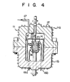
- Seed crystal 35 was gradually lowered into the crucible from the top of the chamber, then was introduced through the B 2 0 3 layer 21 into InP 36, in a molten state as shown in Fig. 4, to make the seed crystal 35 affinitive to the InP 36 (or while adjusting the temperature of molten InP 36 to its affinitive temperature). Finally the seed crystal 35 was gradually pulled up while being rotated, to promote the growth of monocrystal 37.
- the same reference numerals are used to indicate the same component parts shown in Fig. 1.
- the present invention cannot only be applied to the synthesis of GaP and InP, but also to the synthesis of the other Group III element-phosphorus compound crystals, such as Ga 2A sP etc.
- the device used for the synthesis is not limited to the above-mentioned device, as shown in Fig. 1, but any other device can be selectively used.
Landscapes
- Chemical & Material Sciences (AREA)
- Organic Chemistry (AREA)
- Inorganic Chemistry (AREA)
- Engineering & Computer Science (AREA)
- Crystallography & Structural Chemistry (AREA)
- Materials Engineering (AREA)
- Metallurgy (AREA)
- Crystals, And After-Treatments Of Crystals (AREA)
- Liquid Deposition Of Substances Of Which Semiconductor Devices Are Composed (AREA)
Applications Claiming Priority (2)
| Application Number | Priority Date | Filing Date | Title |
|---|---|---|---|
| JP60064427A JPS61222911A (ja) | 1985-03-28 | 1985-03-28 | 燐化化合物の合成方法 |
| JP64427/85 | 1985-03-28 |
Publications (3)
| Publication Number | Publication Date |
|---|---|
| EP0196854A2 true EP0196854A2 (fr) | 1986-10-08 |
| EP0196854A3 EP0196854A3 (en) | 1988-08-10 |
| EP0196854B1 EP0196854B1 (fr) | 1993-11-10 |
Family
ID=13257968
Family Applications (1)
| Application Number | Title | Priority Date | Filing Date |
|---|---|---|---|
| EP86302170A Expired - Lifetime EP0196854B1 (fr) | 1985-03-28 | 1986-03-25 | Méthode de synthèse d'un composé de phosphore et d'un élément du groupe III |
Country Status (5)
| Country | Link |
|---|---|
| US (1) | US4816240A (fr) |
| EP (1) | EP0196854B1 (fr) |
| JP (1) | JPS61222911A (fr) |
| CA (1) | CA1284761C (fr) |
| DE (1) | DE3689272T2 (fr) |
Cited By (4)
| Publication number | Priority date | Publication date | Assignee | Title |
|---|---|---|---|---|
| EP0455325A1 (fr) * | 1990-03-02 | 1991-11-06 | Japan Energy Corporation | Monocristaux de phosphure d'indium semi-isolants et méthode pour leur préparation |
| US5254507A (en) * | 1990-03-02 | 1993-10-19 | Nippon Mining Co., Ltd. | Semi-insulating InP single crystals, semiconductor devices having substrates of the crystals and processes for producing the same |
| EP1013801A1 (fr) * | 1998-12-21 | 2000-06-28 | PIRELLI CAVI E SISTEMI S.p.A. | Procédé et appareillage pour la croissance des cristaux |
| FR2802535A1 (fr) * | 1999-11-19 | 2001-06-22 | Venezia Tecnologie | Procede de synthese directe de phosphure d'indium |
Families Citing this family (3)
| Publication number | Priority date | Publication date | Assignee | Title |
|---|---|---|---|---|
| US6019841A (en) * | 1997-03-24 | 2000-02-01 | G.T. Equuipment Technologies Inc. | Method and apparatus for synthesis and growth of semiconductor crystals |
| CN108358180B (zh) * | 2017-12-08 | 2019-08-02 | 中国电子科技集团公司第十三研究所 | 利用承载气体进行磷化物原位注入合成的方法 |
| CN110760932B (zh) * | 2019-11-22 | 2021-02-23 | 中国电子科技集团公司第十三研究所 | 一种利用铟磷混合物制备磷化铟晶体的方法 |
Family Cites Families (11)
| Publication number | Priority date | Publication date | Assignee | Title |
|---|---|---|---|---|
| DE2060673C3 (de) * | 1969-12-13 | 1980-11-13 | Sony Corp., Tokio | Vorrichtung zur Herstellung von Phosphiden |
| US3704093A (en) * | 1970-06-15 | 1972-11-28 | Little Inc A | Method of synthesizing intermetallic compounds |
| US3777009A (en) * | 1971-08-05 | 1973-12-04 | Little Inc A | Method for direct melt synthesis of intermetallic compounds |
| DE2317797B2 (de) * | 1973-04-09 | 1979-12-06 | Siemens Ag, 1000 Berlin Und 8000 Muenchen | Verfahren zur Herstellung von Galliumphosphid |
| GB2032895B (en) * | 1978-10-25 | 1983-04-27 | Cambridge Analysing Instr | Direct synthesis of inter-metallic compounds |
| US4431476A (en) * | 1981-01-17 | 1984-02-14 | Tokyo Shibaura Denki Kabushiki Kaisha | Method for manufacturing gallium phosphide single crystals |
| US4496424A (en) * | 1982-03-30 | 1985-01-29 | Agency Of Industrial Science & Technology | Method for manufacture of III-V compound semiconducting single crystal |
| JPS58181799A (ja) * | 1982-04-16 | 1983-10-24 | Nippon Telegr & Teleph Corp <Ntt> | 硼素を添加したGaAs単結晶の製造方法 |
| JPS606918B2 (ja) * | 1982-11-02 | 1985-02-21 | 工業技術院長 | 3−5族化合物単結晶の製造方法 |
| JPS606919B2 (ja) * | 1982-11-12 | 1985-02-21 | 工業技術院長 | 3−5族化合物単結晶の製造方法 |
| JPS59131597A (ja) * | 1983-01-18 | 1984-07-28 | Agency Of Ind Science & Technol | 高品質ガリウム砒素単結晶の製造方法 |
-
1985
- 1985-03-28 JP JP60064427A patent/JPS61222911A/ja active Pending
-
1986
- 1986-03-25 DE DE86302170T patent/DE3689272T2/de not_active Expired - Fee Related
- 1986-03-25 EP EP86302170A patent/EP0196854B1/fr not_active Expired - Lifetime
- 1986-03-27 CA CA000505437A patent/CA1284761C/fr not_active Expired - Lifetime
-
1987
- 1987-04-30 US US07/045,774 patent/US4816240A/en not_active Expired - Fee Related
Cited By (5)
| Publication number | Priority date | Publication date | Assignee | Title |
|---|---|---|---|---|
| EP0455325A1 (fr) * | 1990-03-02 | 1991-11-06 | Japan Energy Corporation | Monocristaux de phosphure d'indium semi-isolants et méthode pour leur préparation |
| US5173127A (en) * | 1990-03-02 | 1992-12-22 | Nippon Mining Co., Ltd. | Semi-insulating inp single crystals, semiconductor devices having substrates of the crystals and processes for producing the same |
| US5254507A (en) * | 1990-03-02 | 1993-10-19 | Nippon Mining Co., Ltd. | Semi-insulating InP single crystals, semiconductor devices having substrates of the crystals and processes for producing the same |
| EP1013801A1 (fr) * | 1998-12-21 | 2000-06-28 | PIRELLI CAVI E SISTEMI S.p.A. | Procédé et appareillage pour la croissance des cristaux |
| FR2802535A1 (fr) * | 1999-11-19 | 2001-06-22 | Venezia Tecnologie | Procede de synthese directe de phosphure d'indium |
Also Published As
| Publication number | Publication date |
|---|---|
| JPS61222911A (ja) | 1986-10-03 |
| EP0196854B1 (fr) | 1993-11-10 |
| EP0196854A3 (en) | 1988-08-10 |
| CA1284761C (fr) | 1991-06-11 |
| DE3689272D1 (de) | 1993-12-16 |
| US4816240A (en) | 1989-03-28 |
| DE3689272T2 (de) | 1994-04-21 |
Similar Documents
| Publication | Publication Date | Title |
|---|---|---|
| US7097707B2 (en) | GaN boule grown from liquid melt using GaN seed wafers | |
| EP1540048B1 (fr) | Monocristal de carbure de silicium et procede et dispositif permettant de le fabriquer | |
| JP2001058900A5 (fr) | ||
| EP0460943B1 (fr) | Creuset en nitrure de bore et sa production | |
| JP2001526163A (ja) | 高純度単結晶炭化ケイ素を成長させる方法及び装置 | |
| JP2012067005A (ja) | AlxGa1−xN結晶の成長方法およびAlxGa1−xN結晶基板 | |
| US4816240A (en) | Method of synthesizing Group III element-phosphorus compound | |
| US7621999B2 (en) | Method and apparatus for AlGan vapor phase growth | |
| JP5045232B2 (ja) | AlxGa1−xN結晶の成長方法 | |
| US5524571A (en) | Method for synthesizing compound semiconductor polycrystals and apparatus therefor | |
| EP1132505A2 (fr) | Carbure de silicium monocristallin | |
| KR100358280B1 (ko) | 형광체 및 형광체의 제조방법 | |
| US3899572A (en) | Process for producing phosphides | |
| US8123856B2 (en) | Method and apparatus for producing group III nitride based compound semiconductor | |
| KR20010000827A (ko) | 용융에 의한 지에이엔 단결정 제조방법 | |
| JPS62162694A (ja) | 燐化化合物単結晶の作成方法 | |
| CA1090986A (fr) | Appareil servant a former un compose de groupe ii-vi ou de groupe iii-v | |
| JP2611163B2 (ja) | 化合物半導体結晶の製造方法 | |
| JPH0664905A (ja) | 超高純度セレン化亜鉛の製造方法および装置 | |
| Freyhardt | III–V Semiconductors | |
| JPH0375291A (ja) | ZnSe単結晶の製造方法 | |
| JP2001130999A (ja) | GaAs半導体単結晶製造方法 | |
| JPH09221400A (ja) | ZnSe単結晶の製造方法およびその製造装置 | |
| JPH10167874A (ja) | 化合物半導体単結晶の製造方法 | |
| JPH06172098A (ja) | GaAs単結晶の製造方法 |
Legal Events
| Date | Code | Title | Description |
|---|---|---|---|
| PUAI | Public reference made under article 153(3) epc to a published international application that has entered the european phase |
Free format text: ORIGINAL CODE: 0009012 |
|
| 17P | Request for examination filed |
Effective date: 19860404 |
|
| AK | Designated contracting states |
Kind code of ref document: A2 Designated state(s): DE FR GB |
|
| PUAL | Search report despatched |
Free format text: ORIGINAL CODE: 0009013 |
|
| RHK1 | Main classification (correction) |
Ipc: C01B 25/08 |
|
| AK | Designated contracting states |
Kind code of ref document: A3 Designated state(s): DE FR GB |
|
| 17Q | First examination report despatched |
Effective date: 19890929 |
|
| GRAA | (expected) grant |
Free format text: ORIGINAL CODE: 0009210 |
|
| AK | Designated contracting states |
Kind code of ref document: B1 Designated state(s): DE FR GB |
|
| PG25 | Lapsed in a contracting state [announced via postgrant information from national office to epo] |
Ref country code: FR Effective date: 19931110 |
|
| REF | Corresponds to: |
Ref document number: 3689272 Country of ref document: DE Date of ref document: 19931216 |
|
| EN | Fr: translation not filed | ||
| PLBE | No opposition filed within time limit |
Free format text: ORIGINAL CODE: 0009261 |
|
| STAA | Information on the status of an ep patent application or granted ep patent |
Free format text: STATUS: NO OPPOSITION FILED WITHIN TIME LIMIT |
|
| 26N | No opposition filed | ||
| PGFP | Annual fee paid to national office [announced via postgrant information from national office to epo] |
Ref country code: GB Payment date: 19960318 Year of fee payment: 11 |
|
| PGFP | Annual fee paid to national office [announced via postgrant information from national office to epo] |
Ref country code: DE Payment date: 19960328 Year of fee payment: 11 |
|
| PG25 | Lapsed in a contracting state [announced via postgrant information from national office to epo] |
Ref country code: GB Effective date: 19970325 |
|
| GBPC | Gb: european patent ceased through non-payment of renewal fee |
Effective date: 19970325 |
|
| PG25 | Lapsed in a contracting state [announced via postgrant information from national office to epo] |
Ref country code: DE Effective date: 19971202 |