EP0455428B1 - Circuit logique programmable - Google Patents
Circuit logique programmable Download PDFInfo
- Publication number
- EP0455428B1 EP0455428B1 EP91303771A EP91303771A EP0455428B1 EP 0455428 B1 EP0455428 B1 EP 0455428B1 EP 91303771 A EP91303771 A EP 91303771A EP 91303771 A EP91303771 A EP 91303771A EP 0455428 B1 EP0455428 B1 EP 0455428B1
- Authority
- EP
- European Patent Office
- Prior art keywords
- delay line
- input
- inputs
- outputs
- output
- Prior art date
- Legal status (The legal status is an assumption and is not a legal conclusion. Google has not performed a legal analysis and makes no representation as to the accuracy of the status listed.)
- Expired - Lifetime
Links
- 230000001960 triggered effect Effects 0.000 claims abstract description 29
- 238000007781 pre-processing Methods 0.000 claims abstract description 3
- 230000008878 coupling Effects 0.000 claims description 24
- 238000010168 coupling process Methods 0.000 claims description 24
- 238000005859 coupling reaction Methods 0.000 claims description 24
- 230000000295 complement effect Effects 0.000 claims description 14
- 230000004044 response Effects 0.000 claims description 3
- 230000000903 blocking effect Effects 0.000 claims 2
- 230000009977 dual effect Effects 0.000 abstract description 3
- 230000000630 rising effect Effects 0.000 description 14
- 230000001934 delay Effects 0.000 description 10
- 238000013461 design Methods 0.000 description 9
- 238000010586 diagram Methods 0.000 description 6
- 238000000034 method Methods 0.000 description 6
- 230000001902 propagating effect Effects 0.000 description 5
- 238000013459 approach Methods 0.000 description 4
- 238000005516 engineering process Methods 0.000 description 4
- 230000008569 process Effects 0.000 description 4
- 230000001360 synchronised effect Effects 0.000 description 4
- 230000008859 change Effects 0.000 description 3
- 230000003111 delayed effect Effects 0.000 description 2
- 238000007667 floating Methods 0.000 description 2
- 238000004519 manufacturing process Methods 0.000 description 2
- 238000004549 pulsed laser deposition Methods 0.000 description 2
- 230000003134 recirculating effect Effects 0.000 description 2
- 239000004065 semiconductor Substances 0.000 description 2
- 230000001419 dependent effect Effects 0.000 description 1
- 238000000605 extraction Methods 0.000 description 1
- 208000028560 panic disorder 1 Diseases 0.000 description 1
- 238000003909 pattern recognition Methods 0.000 description 1
- 238000012545 processing Methods 0.000 description 1
- 230000009467 reduction Effects 0.000 description 1
- 229910052710 silicon Inorganic materials 0.000 description 1
- 239000010703 silicon Substances 0.000 description 1
- 238000012360 testing method Methods 0.000 description 1
Images




Classifications
-
- H—ELECTRICITY
- H03—ELECTRONIC CIRCUITRY
- H03K—PULSE TECHNIQUE
- H03K3/00—Circuits for generating electric pulses; Monostable, bistable or multistable circuits
- H03K3/02—Generators characterised by the type of circuit or by the means used for producing pulses
- H03K3/027—Generators characterised by the type of circuit or by the means used for producing pulses by the use of logic circuits, with internal or external positive feedback
- H03K3/037—Bistable circuits
-
- H—ELECTRICITY
- H03—ELECTRONIC CIRCUITRY
- H03K—PULSE TECHNIQUE
- H03K19/00—Logic circuits, i.e. having at least two inputs acting on one output; Inverting circuits
- H03K19/02—Logic circuits, i.e. having at least two inputs acting on one output; Inverting circuits using specified components
- H03K19/173—Logic circuits, i.e. having at least two inputs acting on one output; Inverting circuits using specified components using elementary logic circuits as components
- H03K19/177—Logic circuits, i.e. having at least two inputs acting on one output; Inverting circuits using specified components using elementary logic circuits as components arranged in matrix form
- H03K19/17704—Logic circuits, i.e. having at least two inputs acting on one output; Inverting circuits using specified components using elementary logic circuits as components arranged in matrix form the logic functions being realised by the interconnection of rows and columns
- H03K19/17708—Logic circuits, i.e. having at least two inputs acting on one output; Inverting circuits using specified components using elementary logic circuits as components arranged in matrix form the logic functions being realised by the interconnection of rows and columns using an AND matrix followed by an OR matrix, i.e. programmable logic arrays
-
- H—ELECTRICITY
- H03—ELECTRONIC CIRCUITRY
- H03K—PULSE TECHNIQUE
- H03K5/00—Manipulating of pulses not covered by one of the other main groups of this subclass
- H03K5/15—Arrangements in which pulses are delivered at different times at several outputs, i.e. pulse distributors
- H03K5/15013—Arrangements in which pulses are delivered at different times at several outputs, i.e. pulse distributors with more than two outputs
- H03K5/15026—Arrangements in which pulses are delivered at different times at several outputs, i.e. pulse distributors with more than two outputs with asynchronously driven series connected output stages
- H03K5/1504—Arrangements in which pulses are delivered at different times at several outputs, i.e. pulse distributors with more than two outputs with asynchronously driven series connected output stages using a chain of active delay devices
Definitions
- the invention relates to a combination of programmable logic devices and delay lines.
- synchronous There are two basic approaches to digital electronic circuit design, synchronous and asynchronous.
- the synchronous approach involves clocking registers and other elements once every fixed time period, whereas in the asynchronous approach there is either no clock or many clocks operating at different times.
- Synchronous circuits are reliable and easy to design, since the timing is always fixed, but some speed is sacrificed since the clock period must be set for the slowest component in the system.
- the user can apply successive signals to each component in the system with whatever minimum timing is specified for each respective component. For example, in a typical DRAM controller design, a signal is first applied to a multiplexer to select a row address to be applied to the DRAM. Once the row address stabilizes, the /RAS signal can be applied to the DRAM.
- a signal is then applied to the multiplexer to cause it to select the column address, and when that stabilizes, the /CAS signal is applied to the DRAM.
- the data output of the DRAM stabilizes and may be clocked into a data register.
- control signals can be applied to the respective components with much tighter timing, thereby improving effective DRAM access speed markedly.
- a delay line is an electrical component which provides a predetermined time delay from signal input to signal output.
- Passive delay lines are usually constructed of simple LC networks with no active components, whereas as active delay lines include active drivers to improve reliability, square up the timing signal, and reduce signal attenuation.
- a tapped delay line is a delay line which has several taps, each providing a signal at successively increasing time periods from the time that the signal is initially applied to the delay line input. Examples of tapped delay lines are the DS100, DS1005, DS1007 and DS1010 series of silicon delay lines manufactured by Dallas Semiconductor.
- Prior-art delay lines are typically fixed upon manufacture and not adjustable by the user. Users who require delays other than those available on standard parts therefore must either have custom delay lines manufactured or be satisfied with non-optimum delays. Dallas Semiconductor will set the delay times of its DS1007 according to a customer's specifications, but this setting must be done at the factory. The inability of users to change the delays in the field can slow design cycles and generate wasted devices if the user's needs change. Users also need to purchase a variety of different delay lines to cover all applications, which increases inventory and production costs. Devices are available which include a fixed tapped delay line, with a user-addressed multiplexer to select which delay tap is to be gated out.
- This method offers more flexibility, but is pin-intensive and still requires a large number of devices to obtain a plurality of different delayed signals.
- User-adjustable VCO-based analog delay generators also exist, but they are much more complicated and more costly than a string of delay elements.
- a third problem is that existing tapped delay lines are limited by either resolution or total delay. With fine resolution and a limited number of output pins, only a limited number of taps can be placed and the total delay will be small. On the other hand, if the total delay is long, then the resolution may be too coarse. Several delay line devices are therefore usually required if long delays with fine resolution are desired. Multiple delay lines can be costly, can add skew, can add to board space and power consumption problems, and may cause monotonicity problems.
- US-A-3987410 is directed to hardware used for feature extraction and pattern recognition.
- character data is passed entirely through a large number of shift registers and then fed into programmable logic circuitry for a determination of the pattern presented by the character data.
- the reference does not disclose a connection array means of the type as set out in claim 1. Instead the delay line taps SR1-SR48 are in fact delay line outputs. The taps are all coupled directly to the programmable logic circuitry PAND1-PAND48. No means is provided for coupling the delay line outputs to selected ones of the delay line taps.
- the present invention provides a programmable logic device comprising:
- the flip flops preferably comprise multiple-set, multiple-reset, edge-triggered set/reset flip flops, each of the inputs of which are connected to a respective array output.
- the flip flops Preferably, the flip flops have two set and two reset inputs each. Having edge-triggered outputs makes the output signals independent of the width of pulses propagating down the delay lines. Having them as set/reset flip flops permits easy implementation of assert/negate logic, and including multiple-set and multiple-reset inputs makes it unnecessary to ensure that one set (reset) condition is turned off before the next occurs.
- a tapped delay which feeds a programmable logic array, an output of which can feed the input of the delay line.
- the trigger input of the delay line can derive either from the output of the array or from an external source, or be selectable between those sources.
- Providing the ability to drive the delay line trigger from an array output both permits economical and low-skew logic for the trigger signal, and also permits recirculating delay signals.
- a recirculating delay signal can be used to generate very long delays without loss of resolution.
- the programmable array is preferably a programmable combinatorial array, and preferably a programmable AND array followed by a fixed OR array. This permits programming of nearly any desired logic function or functions as a result of the timing signals from selected taps of the delay line and/or from external input signals to the array, all with minimal skew.
- the delay line may have a large number of finely spaced taps, and may be included in a delay line macrocell which has a certain number of outputs feeding the array.
- the delay line macrocell has fewer outputs than there are taps in the delay line.
- a programmable connection array may then be provided to connect any one of the delay line macrocell outputs to any desired tap of the delay line.
- a second delay line may also be included in the delay line macrocell, the taps of which may provide additional inputs to the connection array.
- Cascading logic may be included in a delay line macrocell for cascading the two delay lines together or, selectably, applying a separate input signal to the trigger of the second delay line. Like the trigger to the first delay line, the trigger to the second delay line may be selected from an external source or from an output of the array.
- the delay line outputs may be applied to the array directly or, alternatively, may be preprocessed through array driving circuitry.
- the array driving circuitry preferably comprises a 2-input AND gate, one of the inputs of which is a non-inverting input connected to a first one of the macrocell outputs.
- the other AND gate input is an inverting input which is connected programmably to a second one of the macrocell outputs. Accordingly, if the second input is programmed to connect to the second macrocell output, then the AND gate output will be a precisely defined window pulse. If the second input is so programmed and the first macrocell output is programmed within the connection array to V cc (logic high or 1), then the output of the AND gate is an inverted version of the signal on the second macrocell output. And if the second input of the AND gate is disconnected from the second macrocell output, then the first macrocell output effectively drives the array directly.
- Fig. 1 Shown in Fig. 1 is a block diagram of apparatus according to the invention. It is fabricated on a single chip 10, and comprises a programmable combinatorial logic array 12, output circuitry 14, a delay line macrocell 16, and array driving circuitry 18.
- the combinatorial array 12 includes a programmable AND array 20 followed by a fixed OR array 22, but the OR array 22 can instead be made programmable. It is well known in the art that though a programmable combinatorial logic array may be described at an architectural or logic level as an AND/OR array, the actual implementation at the transistor level may be NAND/NAND, NOR/NOR, or some other related combination.
- a programmable combinatorial logic array also may or may not include complementary drivers on its inputs.
- a plurality of input lines 24 to the combinatorial array 12 connect to package leads 25, and pass through a respective plurality of complementary drivers 26 before being provided to the AND array 20. Other inputs to the AND array are described below.
- the OR array 22 has a plurality of outputs which feed the output circuitry 14, outputs of which are connected over lines 28 to package leads 29.
- the output circuitry 14 also generates a plurality of feedback signals over lines 30, which feed back to the AND array 20 via respective complementary drivers 32.
- Another output 36 of the combinatorial array 12, this output taken directly from the AND array 20, is provided to an INIT input of the output circuitry 14 and performs a function described below.
- the delay line macrocell 16 has three inputs and a plurality of outputs.
- the TR1 input of delay line macrocell 16 is connected to the output of a 2:1 multiplexer 40, one input 42 of which is connected to an output of OR array 22.
- the other input of multiplexer 40 is connected over a line 44 to a package pin 45, which is also connected via a complementary driver 46 to inputs of the AND array 20.
- the selection made by multiplexer 40 is controlled by a programmable fuse 48.
- Input TR2 to delay line macrocell 16 is connected to the output of another 2:1 multiplexer 50, one input 52 of which is connected to another output of OR array 22.
- the other input of multiplexer 50 is connected over a line 54 to a package lead 55, which is also connected through a complementary driver 56 to inputs of the AND array 20.
- the selection made by multiplexer 50 is controlled by a programmable fuse 58. All programmable fuses in the embodiment of Fig. 1 are in fact EECMOS floating gate cells, but any other technology may be used instead, including but not limited to, fuse, anti-fuse, other floating gate technology, mask or even volatile technology such as RAM and latches.
- fuses For convenience, all these technologies are referred to herein as "fuses.” Further, though various selections outside the combinatorial array 12 are shown as being fuse programmable, many of them can instead be selected by an output of the array 12.
- the programmable elements on the device 10 are programmed through the use of conventional programming circuitry 90.
- a BLK input to delay line macrocell 16 is connected to an array output 60, deriving directly from the AND array 20. (Note that the BLK input can instead come from the output of an OR gate). The function of the BLK input is described below.
- delay line macrocell 16 The outputs of delay line macrocell 16 are connected to inputs of array driving circuitry 18, the outputs of which are connected over lines 64 to inputs of the AND array 20.
- One of the outputs, 65, of delay line macrocell 16 is also connected through a three-state buffer 66 to a bi-directional package pin 67 which is also connected over a line 70 and through a complementary driver 72 to inputs of the AND array 20.
- Programmable fuse 68 controls the output enable of three-state buffer 66. If the buffer 66 is enabled, then package lead 67 directly outputs the signal on delay line macrocell output 65. The signal is also fed back into the AND array 20 via driver 72. If the buffer 66 is disabled, then the package lead 67 becomes another input to the AND array 20 via driver 72.
- Combinatorial array 12 is shown in Fig. 1 as a programmable AND array followed by a fixed OR array, with some complementary and some non-complementary inputs to the AND array.
- Other fuse- or mask-programmable logic structures would also suffice.
- the multiplexer 40 selects a trigger signal either directly from the package lead 45 or from array output 42 to apply to the first trigger input (TR1) of delay line macrocell 16.
- TR1 first trigger input
- the delay line macrocell 16 contains a plurality of sequentially coupled active delay elements, taps from which are coupled to outputs of the delay line macrocell 16. A preferred embodiment for the delay line macrocell 16 is described below.
- the outputs of delay line macrocell 16 are waveforms that replicate the signal on the TR1 input after respective known delays.
- delay line macrocell 16 can also include a second independent delay line whose taps can also be coupled to outputs of delay line macrocell 16.
- TR2 is the trigger input for the second delay line.
- the outputs of delay line macrocell 16 pass through optional array driving circuitry 18 before being provided on lines 64 to inputs of the combinatorial array 12.
- array driving circuitry 18 Various embodiments for the array driving circuitry 18 are described below, but essentially, the array driving circuitry 18 provides a certain amount of preprocessing of the delayed signals from the delay line macrocell 16 in order to improve their usefulness in the array 12.
- One of the outputs 65 of delay line macrocell 16 can be routed directly to a package lead via three-state buffer 66, in order to provide a direct output from the delay line macrocell 16.
- This output has extremely small skew since it passes through a minimum amount of logic before being provided to the lead, and is useful for extremely time-sensitive edges.
- the direct output is also useful for cascading delay line PLDs together.
- Polarity selection means such as an XOR gate, can be added in this output path if desired, at the risk of some additional skew.
- the output circuitry 14 preferably includes a plurality of edge-triggered devices, the outputs of which are "asserted” when an effective edge arrives from one output of the combinatorial array 12 and “negated” when an effective edge of a different output of the combinatorial array 12 arrives. In this way, the timing of both the assertion and negation of each output signal on lines 28 can be controlled by the logic in the combinatorial array 12. If the timing of the negation of a signal is not important, then a combinatorial path may be included in the output circuitry 14 for providing a combinatorial array output directly to one of the output leads on one of the lines 28.
- the output circuitry 14 also generates signals on line 30 which are fed back to the combinatorial array.
- the feedback feature permits the assertion or negation of an output signal to be dependent upon when the output signal actually was negated or asserted at some point in the past.
- the feedback feature also permits the array to alter the timing of trigger signals applied to the delay line macrocell 16, and permits the array to lengthen the effective delay upon certain conditions, and qualify whether and when to trigger the delay line macrocell again.
- Output circuitry 14 includes a plurality of edge-triggered set/reset flip flops 100a and 100b, each with two edge-triggered set inputs (S1 and S2) and two edge-triggered reset inputs (R1 and R2) and an output (Q).
- the edge-triggered inputs to set/reset flip flop 100a are each connected to the output of a respective OR gate 102a in the OR array 22, and the edge-triggered inputs to set/reset flip flop 100b are connected to the outputs of respective OR gates 102b in the OR array 22.
- OR gates 102a sum together three product terms each, whereas OR gates 102b sum together two product terms each.
- the edge-triggered inputs of others of the set/reset flip flops 100a and 100b, as well as others not shown in Fig. 2 are also connected to the outputs of an assortment of 2- and 3-input OR gates (not shown) in OR array 22.
- Each of the set/reset flip flops 100a and 100b also has an INIT input, and all of the INIT inputs are commonly connected to the product term output 36 of the AND array 20. (Note that INIT input can also come from an OR gate output.)
- INIT input can also come from an OR gate output.
- each of the flip flops 100a and 100b is asynchronously initialized to the value specified on its respective AP/0A0C input.
- the AP/0A0C input is determined separately for each of the flip flops 100a and 100b by a respective fuse 104.
- the Q output of each of the flip flops 100a and 100b is connected through a respective driver 106a and 106b to respective package output leads 29.
- the Q outputs are also fed back over lines 30 and through complementary drivers 32 into inputs of the AND array 20.
- Others of the flip flops 100 not shown in Fig. 2 omit the feedback signal. No 0Q is needed for the flip flops 100, since if an active low output is desired, the user need only interchange the product term formulas for the set inputs of the set/reset flip flops with the product term formulas for the reset inputs of the flip flops and program the AP/0A0C fuse appropriately. It should be noted that other prior-art features can also be added to the output circuitry 14.
- the drivers 106a and 106b can be made three-state, the enable through which can be controlled by a fuse, and a feedback multiplexer can be placed in the feedback paths 30 to select either the Q output of a flip flop or the signal on the pin 29 for feeding back to the array.
- Each of the set/reset flip flops is designed so as to minimize skew between the various edge-triggered inputs. That is, the time delay from an edge on any of the four edge-triggering inputs to the Q output is virtually equal for any of the edge-triggering inputs. In this way falling edges on the Q output can be timed just as precisely by the circuit of Fig. 1 as rising edges.
- the circuit is also designed to have a small settling time in order to avoid any uncertainty which may arise when two triggering edges occur within a short time of each other. Further, the circuit is designed such that a rising edge on either set input while the Q output is low will cause a rising edge on the Q output even if the other set input is still high from a previous rising edge.
- a dual edge-triggered, set/reset flip flop which satisfies the above criteria is shown in Fig. 3.
- the output drivers 106a and 106b in order to minimize skew between rising and falling edges, should be balanced such that the rise time from the minimum output voltage to the threshold voltage is equal to the fall time from the maximum output voltage down to the threshold voltage.
- speed should be emphasized in the combinatorial array 12 for rising edges rather than being designed for a compromise between rising and falling edges.
- the combinatorial array 12 should also be as fast as possible to avoid array-related skews. In general, the faster the device is, the less skew it will have.
- FIG. 4 shows one option, in which two outputs 120 and 122 of the combinatorial array are first selectably inverted by respective XOR gates 124 and 126 controlled by respective fuses 128 and 130, before being provided to respectively the set and reset inputs of a single-set/single-reset edge-triggered flip flop 132.
- An INIT input is provided from the combinatorial array 12, and a fuse 134 is coupled to an AP/0A0C input of the flip flop 132.
- the fuse 134 selects whether the INIT input operates as an asynchronous preset or asynchronous clear of the Q output of the flip flop 132.
- the Q output of the flip flop 132 is provided through a driver 136 to a package lead 28.
- XOR gates 124 and 126 permits the user to select either rising or falling edge triggering for each edge-triggering input of the set/reset flip flop.
- it also adds an additional layer of logic between the delay line outputs and the edge triggering flip flop inputs, therefore increasing the risk of skew.
- Polarity control on the combinatorial AND/OR array outputs also is useful for minimizing the number of product terms required for the trigger condition, so that by using DeMorgan's theorem, more complex logic functions can be implemented with a limited number of product terms.
- Fig. 5 shows another arrangement for output circuitry 14, in which 2T edge-triggered flip flops 140 are substituted for the dual or single edge-triggered, set/reset flip flops of Figs. 3 and 4.
- a rising edge on either trigger input causes the Q output to toggle, regardless of the state of the other T input.
- fuse-programmable XOR gates are provided between the array outputs and the edge-triggered inputs of the flip flop 140, an INIT input is connected to a combinatorial array output, a fuse-programmable AP/0A0C input is provided, and the Q output is coupled through a driver 142 to a package lead 28.
- AS and AR inputs to the flip flop 140 are connected to respective outputs of the combinatorial array for asynchronously setting or resetting the Q output.
- 2T edge-triggered flip flops are useful for creating multiple output pulses, but generally require the AS and AR inputs in order to hold the state of the flip flop to avoid unwanted toggling, or to force assertion or negation regardless of the prior state.
- output circuitry 14 can contain two or more different types of output flip flops. If so, it is desirable that they all be variations of a single basic circuit design in order to minimize skews from one output to another.
- the output circuitry 14 can also contain other types of registers, such as D flip flops and latches.
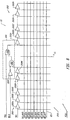
- Fig. 6 shows a detail of the delay line macrocell 16 (Fig. 1). It comprises two strings 200 and 202 of serially coupled delay elements 200a-200n and 202a-202n, respectively. Each string contains 30 of the delay elements, and each delay element represents a highly accurate compensated 5 nanosecond time delay.
- the delay line macrocell 16 further includes a connection array 210 which can programmably connect any of the taps from either of the two delay line strings 200 and 202 to any of eight delay line macrocell outputs DELAY0-DELAY7. Other numbers of outputs, for example 16, may also be provided. Taps are taken from the output of each delay element in each of the two strings 200 and 202, as well as from the input of the first delay element 200a and 202a in each of the strings.
- Each of the delay line outputs DELAY0-DELAY7 can also be connected in the connection array 210 to V cc . This feature is useful for some of the alternatives for array driving circuitry 18, described below.
- each tap from the delay lines 200 and 202 can be coupled to only one of the delay line outputs DELAY0-DELAY7, and each of the delay line outputs DELAY0-DELAY7 can be coupled to only one signal source (e.g., only one of the delay line taps or V cc ).
- more than one delay line tap can be programmably coupled to any given one of the delay line outputs. In such a situation, the selected delay line taps should be logically ORed to produce the delay line output signal. More than one delay line output can be programmably coupled to a single signal source as well in a different embodiment, but this flexibility is not needed inside the macrocell if equivalent flexibility is provided outside the macrocell.
- the output of delay element 200n in string 200 is also coupled through cascading logic 220 to provide the input signal for the second string 202.
- cascading logic 220 the output of delay element 200n is connected to one input of a two-input AND gate 222, the other input of which is connected to the output of an inverter 224.
- the input of inverter 224 is connected to the BLK input (Fig. 1) of delay line macrocell 16.
- the output of AND gate 222 is connected to one input of a two-input OR gate 226, the other input of which is connected to the TR2 input (Fig. 1) of the delay line macrocell 16.
- the output of OR gate 226 is the output of cascading logic 220, and is connected to the input of delay element 202a.
- the cascading logic 220 shown in Fig. 6 is one example of cascading logic for coupling two delay lines together, and many other designs are possible.
- another possible implementation of cascading logic 220 is as a simple multiplexer in which an external select input selects whether the input to the second delay line 202 will come from the output of the first delay line 200 or from the TR2 input of the delay line macrocell 16.
- the embodiment shown for cascading logic 220 in Fig. 6 is preferred, however, since while allowing cascading of the two delays lines, it can still potentially accept triggering pulses from another source (TR2).
- delay line macrocell 16 shown in Fig. 6 includes two delay lines optionally cascaded together, a different embodiment may include only one delay line, or may include more than two. In order to reduce risks associated with any asymmetry, all of the tap delays should be equal and the number of delay elements in each of the delay lines in the delay line macrocell 16 should be equal. However, in a different embodiment, different tap delays or different numbers of delay elements may be provided.
- the delay line elements 200a-200n and 202a-202n should be individual active delay elements so as to permit the user to start a new signal down the line before an earlier signal reaches the end of the line. This is a technique useful for pipelined asynchronous control schemes. Also, the rise and fall time for the output of each delay element should be the same, in order to prevent shrinkage or expansion of pulses as they are transmitted down the delay. Further, the delay lines should be able to accept short triggers, for high and low duration, in order to facilitate tighter pipeline timing. Finally, the time delay of the delay elements should not change as a result of either temperature variations or chip-to-chip process variations.
- each of the delay elements 200b-200n and 202b-202n are identical and are constructed according to the circuit of Fig. 7.
- the voltage references 254 and 256 for all of the delay elements 200 and 202 are generated by a programmable reference current source as shown in Fig. 8.
- the circuits of Figs. 7 and 8 are both described in detail in the related application and will not be further described here.
- the programmable reference current source of Fig. 8 is inherently temperature compensating, and each chip can be individually compensated for process variations by programming the electrically erasable fuses F1, F2 and F3. Though any of the other fuses in the device of Fig. 1 can be made mask programmable, the fuses F1, F2 and F3 would not be made mask programmable if they are to be used to compensate for process variations between different chips.
- the entire delay Iine macrocell 16 should preferably be laid out in a very regular manner, tightly coupled to avoid skews.
- the macrocell should be separated from the remainder of the circuit for noise reduction and it may be desirable further to include a noise guard around the macrocell and to incorporate large ground and V cc buses.
- the delay line macrocell 16 shown in Fig. 6 is only one example of a delay line macrocell usable with the invention. In another embodiment, only one delay line of 30 delay elements is included, and only a single trigger input is provided.
- a KILL input (shown dotted in Fig. 6) may also be provided to force any signal propagating down the delay line to a known voltage (such as zero). If provided, the KILL input should be connected to one of the outputs of the combinatorial array 12.
- the KILL capability would allow the user to speed up a system in some applications, and is most useful in delay line implementations which do not permit more than one pulse to be propagating down the line at the same time.
- the KILL feature may also be implemented in such a way that it simply blocks further propagation of a signal beyond a programmably selectable tap in the delay line.
- one of the possible inputs to the TR1 or TR2 inputs to delay line macrocell 16 comes from an output of the combinatorial array 12. If the combinatorial array 12 is organized as a programmable AND and a fixed OR array, it is desirable to derive these trigger input signals from respective sum terms.
- One (secondary) product term for the sum should be programmed to mask any glitches that might appear on another (primary) product term, thereby avoiding false triggering of the delay line macrocell 16 by the primary product term. Additional product terms are also useful if it is desired to be able to start pulses down a delay line on more than one condition.
- one of the outputs 65 of delay line macrocell 16 in addition to being coupled to the array driving circuitry 18, is also couplable through a three-state buffer 66 to a package lead.
- Such a direct output tap is usually not necessary, since all the logic to which it would otherwise be connected should now be programmable into the combinatorial array 12.
- the direct output tap is useful, however, for testing and for cascadability of multiple delay line PLDs.
- array driving circuitry 18 One option for array driving circuitry 18 is to have a simple, active-high driver coupling each delay line macrocell output to a respective input of the combinatorial array 12. This option minimizes skews, but leaves all signal processing to the combinatorial array 12.
- the array driving circuitry consists of a complementary driver coupling each delay line macrocell output to respective pairs of complementary inputs to the combinatorial array 12.
- Fig. 9b Another option, shown in Fig. 9b, comprises a plurality of 2-input XOR gates, the inputs of which are coupled to respective pairs of the delay line macrocell outputs. The outputs of each of the XOR gates are then coupled through a complementary driver to a respective pair of inputs to the combinatorial array 12.
- the arrangement of Fig. 9b is useful for generating pulses having accurate widths.
- the user would program the connection array 210 such that two of the delay line macrocell outputs (e.g., DELAY0 and DELAY1) connect to selected taps of one of the delay lines. As an edge propagates down the delay line, then, one of the delay line macrocell outputs will switch before the other.
- the XOR gate in array driving circuitry 18 will then output a logic 1 for only the time period between the two selected taps. The user must be careful, however, since a pulse will appear on the output of the XOR gate also in response to the trailing edge of a pulse propagating down the delay line.
- the embodiment shown in Fig. 9d comprises a plurality of 2-input AND gates, one input of which is inverting and the other input of which is non-inverting, and the outputs of which are coupled via respective complementary drivers into the combinatorial array 12.
- the inputs to the AND gates are connected to respective pairs of outputs of the delay line macrocell 16.
- this arrangement is also useful for generating pulses having an accurate duration. This arrangement, however, generates such pulses only on one edge of a pulse propagating down the delay line.
- the embodiment shown in Fig. 9c comprises a plurality of AND gates each having an inverting and a non-inverting input, the output of each of the AND gates driving the combinatorial array through a respective non-inverting buffer.
- Each of the delay line macrocell outputs except for DELAY0 and DELAY7, is connected both to the non-inverting input of one AND gate and the inverting input of another AND gate, such that each of the AND gates has its non-inverting input connected to one delay line macrocell output and its inverting input connected to another.
- the DELAY0 output of delay line macrocell 16 is connected only to the non-inverting input of the AND gate whose inverting input is connected to the DELAY1 output, and the DELAY7 output of the delay line macrocell 16 is connected only to the inverting input of the AND gate whose non-inverting input is connected to the DELAY6 output.
- the DELAY7 output of the delay line macrocell 16 is also coupled through its own dedicated, non-inverting buffer to an input of the combinatorial array.
- the arrangement of Fig. 9c is essentially the same as that of Fig. 9d, with the addition of some functionality provided by three additional AND gates. The outputs of the three added AND gates are provided as additional inputs to the combinatorial array 12.
- Fig. 9e shows yet another embodiment for array driving circuitry 18. It is identical to the arrangement of Fig. 9c, except that the connection between each of the delay line macrocell outputs and an inverting input of an AND gate is programmable. In particular, if the fuse is disconnected, then a logic 0 is applied to the inverting input of the AND gate, effectively causing it to pass the non-inverting input signal directly through. Thus, if the user disconnects one of the fuses, say, fuse 280, then AND gate 282 and buffer 284 will pass the DELAY1 output signal from delay line macrocell 16 directly into the combinatorial array 12.
Landscapes
- Physics & Mathematics (AREA)
- Mathematical Physics (AREA)
- Nonlinear Science (AREA)
- Engineering & Computer Science (AREA)
- Computer Hardware Design (AREA)
- Computing Systems (AREA)
- General Engineering & Computer Science (AREA)
- Logic Circuits (AREA)
- Pulse Circuits (AREA)
Claims (32)
- Dispositif logique programmable comprenant :- un circuit logique programmable (12) possédant des entrées et des sorties (14);- un macrobloc à ligne à retard (18) possédant une entrée de ligne à retard, une pluralité de prises à lignes à retard et une pluralité de sorties de ligne à retard;caractérisé par un moyen de groupement de connexion (210) destiné à coupler par programmation chacune desdites sorties de ligne à retard (RETARD 0-RETARD 7) à une prise sélectionnée parmi celles à lignes à retard; et- un moyen de commande de circuit (18) pour coupler ces sorties de ligne à retard à un sous-ensemble desdites entrées de circuit.
- Appareil selon la revendication 1, dans lequel le circuit logique programmable (12) est un circuit combinatoire, comprenant en outre une bascule RS (100a, 100b) ayant au moins une entrée de mise à 1 déclenchée par front d'impulsion, au moins une entrée de mise à zéro déclenchée par front d'impulsion et une sortie, chacune des entrées de cette bascule étant couplée à une sortie respective de circuit.
- Appareil selon la revendication 2, dans lequel la bascule RS (100a, 100b) possède deux entrées de mise à 1 et deux entrées de mise à zéro déclenchées par front d'impulsion, chacune des entrées de cette bascule étant couplée à une sertie respective de circuit, cette bascule en cours d'utilisation, mettant à 1 sa sortie si un front prédéterminé d'impulsion est reçu par l'une quelconque des entrées de mise à 1 quand ladite bascule est remise à zéro, et remettant à zéro sa sortie si un front prédéterminé d'impulsion est reçu par l'une quelconque des entrées de mise à zéro quand ladite bascule est mise à 1.
- Appareil selon la revendication 1, comprenant en outre un moyen de couplage d'entrée de ligne à retard (40, 50) pour coupler une des sorties de circuit à cette entrée de ligne à retard.
- Appareil selon la revendication 4, dans lequel le moyen de couplage d'entrée de ligne à retard (40, 50) couple de manière réversible une des sorties de circuit avec un autre signal (45, 56) à ladite entrée de ligne de retard.
- Appareil selon la revendication 1, comprenant en outre :- une sortie de boîtier (45, 55) couplée à l'une des entrées de circuits; et- un moyen de couplage d'entrée de ligne à retard (40, 50) pour coupler de manière réversible ladite entrée à cette sortie de bottier (45, 55) ou à l'une des sorties de circuit (42, 52).
- Appareil selon la revendication 1, dans lequel ledit macrobloc à ligne à retard (16) comprend :- une première pluralité de premiers éléments à retard (200) couplés en série, chacun ayant une entrée et une sortie, l'entrée du premier de ces premiers éléments étant couplée de manière à recevoir l'entrée de ligne à retard; et- ledit moyen de groupement de connexion (210) pour coupler de manière réversible chacune des sorties de ligne à retard au moins à la sortie de l'un quelconque des premiers éléments à retard.
- Appareil selon la revendication 7, dans lequel le moyen de connexion (210) est en outre destiné à coupler de manière réversible chacune des sorties de ligne à retard à l'entrée de ligne à retard.
- Appareil selon la revendication 7, dans lequel le moyen de connexion (210) est en outre destiné à coupler de manière réversible chacune des sorties de ligne à retard à une logique 1 (Vcc).
- Appareil selon la revendication 7, dans lequel le macrobloc à ligne à retard comprend en outre une seconde pluralité de seconds éléments à retard couplés en série (202), chacun ayant une entrée et une sortie, et dans lequel le moyen de connexion (210) est en outre destiné à coupler de manière réversible chacune des sorties de ligne à retard à la sortie de l'un quelconque des seconds éléments à retard.
- Appareil selon la revendication 1, dans lequel le macrobloc à ligne à retard comprend :- une première (200) et une seconde (202) pluralité d'éléments à retard couplés en série, chacun de ces éléments ayant une entrée et une sortie, l'entrée du premier élément à retard de la première pluralité étant couplée de manière à recevoir ladite entrée de ligne à retard;- ledit moyen de groupement de connexion (210) pour coupler de manière réversible chacune desdites sorties de ligne à retard à la sortie de tout élément à ligne à retard; et- un moyen de mise en cascade (220) pour coupler la sortie du dernier élément à retard de la première pluralité à l'entrée du premier élément à retard de la seconde pluralité.
- Appareil selon la revendication il, dans lequel le moyen de mise en cascade (220) couple de manière réversible la sortie du dernier élément à retard de la première pluralité avec un autre signal à l'entrée du premier élément à retard de la seconde pluralité.
- Appareil selon la revendication 11, dans lequel le macrobloc à ligne à retard (18) possède en outre une entrée de blocage (60), et le moyen de mise en cascade (220) empêche les sorties du dernier élément à retard de la première pluralité d'atteindra l'entrée du premier élément à retard de la seconde pluralité en réponse à un signal sur cette entrée de blocage.
- Apparell selon la revendication 1, dans lequel le macrobloc à ligne à retard comprend en outre :- une entrée d'interruption (KILL); et- un moyen pour forcer chacune des prises à ligne à retard à une valeur prédéterminée en réponse à un signal sur ladite entrée d'interruption.
- Appareil selon la revendication 14, dans lequel l'entrée d'interruption est couplée à l'une desdites sorties de circuit.
- Appareil selon la revendication 1, comprenant en outre une sortie de boîtier (67) et des moyens programmables (66, 68) pour coupler l'une des sorties de ligne à retard à cette sortie de boîtier.
- Appareil selon la revendication 1, dans lequel le moyen de commande de circuit comprend un moyen pour coupler chacune des sorties de ligne à retard aux entrées respectives de circuit.
- Appareil selon la revendication 1, dans lequel ledit moyen de commande de circuit (18) comprend :- une pluralité de portes logiques, chacune ayant une pluralité d'entrées et une sortie, chacune de ces entrées étant couplée à une sortie respective de ligne à retard; et- un moyen pour coupler les sorties des portes logiques audit sous-ensemble de sorties de circuit.
- Appareil selon la revendication 18, dans lequel les portes logiques sont des portes OU exclusif.
- Appareil selon la revendication 18, dans lequel chacune des portes logiques est une porte ET ayant une entrée inverseuse et une entrée non inverseuse.
- Appareil selon la revendication 1, dans lequel le moyen de commande de circuit comprend :- une pluralité de portes logiques, chacune ayant une pluralité d'entrées et une sortie, chacune desdites sorties de ligne à retard étant couplée aux sorties d'au moins deux des portes logiques; et- un moyen pour coupler les sorties de ces portes logiques audit sous-ensemble d'entrées de circuit.
- Appareil selon la revendication 21, dans lequel chacune des portes logiques est une porte ET ayant une entrée inverseuse et une entrée non inverseuse, et dans lequel chacune des sorties de ligne à retard est couplée à l'entrée non inverseuse de l'une des portes ET et l'entrée inverseuse d'une autre des portes ET,
- Appareil selon la revendication 1, dans lequel le moyen de commande de circuit comprend :- une porte logique ayant au moins deux entrées et une sortie, une de ces entrées étant couplée à l'une desdites sorties de ligne à retard et une autre de ces entrées étant couplée par programmation à une autre des sorties de ligne à retard; et- un moyen pour coupler la sortie de la porte logique à l'un des sous-ensembles d'entrées de circuit.
- Appareil selon la revendication 1, comprenant en outre un moyen de commande de circuit logique pour prétraiter au moins un sous-ensemble des prises à ligne à retard afin d'alimenter au moins un sous-ensemble d'entrées de circuit logique programmable.
- Appareil selon la revendication 24, comprenant en outre :- une pluralité de sorties de boîtier; et- un ensemble de circuits de sortie ayant des entrées et des sorties, ces sorties étant couplées à ces sorties de boîtier,dans lequel le circuit logique de groupement programmable possède en outre des entrées supplémentaires couplées aux sorties de boîtier et des sorties supplémentaires couplées aux entrées de cet ensemble de circuits de sortie.
- Appareil selon la revendication 24, dans lequel le moyen de commande de circuit logique comprend un premier moyen pour déclencher une première desdites prises avec une seconde de ces prises afin d'alimenter une première desdites entrées vers le circuit logique programmable.
- Appareil selon la revendication 26, dans lequel le moyen de commande du circuit logique comprend en outre un second moyen pour déclencher une troisième desdites prises avec une quatrième de ces prises afin d'alimenter une seconde desdites entrées, vers le circuit logique programmable.
- Appareil selon la revendication 26, dans lequel le moyen de commande de circuit logique comprend en outre un second moyen pour déclencher ladite seconde prise avec une troisième de ces prises afin d'alimenter une seconde desdites entrées vers le circuit logique programmable.
- Appareil selon la revendication 28, dans lequel le premier moyen de transmission comprend une première porte ET ayant une entrée non inverseuse, une entrée inverseuse et une sortie, cette sortie étant couplée à la première des entrées vers le circuit logique programmable l'entrée non inverseuse pouvant être couplée par programmation à la première desdites prises et l'entrée inverseuse pouvant être couplée par programmation à la seconde desdites prises ou à un zéro logique, et dans lequel le second moyen de transmission comprend une seconde porte logique ET ayant une entrée non inverseuse, une entrée inverseuse et une sortie, cette sortie étant couplée à la seconde desdites entrées vers le circuit logique programmable, l'entrée non inverseuse pouvant être couplée par programmation à la seconde desdites prises et l'entrée inverseuse pouvant être couplée par programmation à la troisième desdites prises ou à un zéro logique.
- Appareil selon la revendication 26, dans lequel le premier moyen pour déclencher une première desdites prises avec une seconde de ces prises comprend un moyen pour sélectionner par programmation cette première et cette seconde prise parmi la pluralité de prises à ligne à retard.
- Appareil selon la revendication 30, dans lequel le premier moyen de transmission comprend en outre un moyen pour sélectionner par programmation la première et la seconde prise à partir d'une entrée de la ligne à retard ou une logique 1.
- Dispositif logique programmable comprenant :- un macrobloc à ligne à retard (16) contenant une première (200) et une seconde (202) chaîne ou des premiers et seconds éléments actifs à retard couplés en série et une matrice de connexion programmable (210) ayant des entrées et des sorties, ces entrées étant couplées de manière à respectivement recevoir la sortie de chacun des éléments à retard, l'entrée du premier élément à retard de chaque chaîne, et une logique 1 (Vcc), ces sorties de matrice de connexion alimentant les sorties du macrobloc à ligne à retard;- un ensemble de circuits de commande de matrice (18) comprenant une pluralité de portes, chacune de ces portes ayant une entrée inverseuse une entrée non inverseuse et une sortie, chacune de ces entrées étant couplée de manière à recevoir une sortie du macrobloc, au moins une des sorties de ce macrobloc étant couplée à l'entrée inverseuse de l'une desdites portes et l'entrée non inverseuse d'une autre de ces portes;- un circuit logique combinatoire programmable (12) comprenant une matrice ET programmable (20) suivie par une matrice OU fixe (22), cette matrice ET ayant des sorties couplées de manière à recevoir les sorties desdites portes dans l'ensemble de circuits de commande de matrice, ce moyen logique combinatoire programmable comprenant en outre des sorties de la matrice ET et des sorties de la matrice OU;- une pluralité de sorties de boîtier (45, 55);- un premier et un second multiplexeur (10, 50) ayant chacun des première et seconde entrées respectives et une sortie, et chacun ayant en outre une entrée de sélection, ces dernières étant couplées de manière à recevoir l'une sortie respective de la matrice OU et lesdites secondes entrées étant couplées à l'une sortie respective de boîtier, la sortie du premier multlplexeur étant couplée à l'entrée de la première chaîne d'éléments à retard du macrobloc à ligne à retard et la sortie du second multlplexeur étant couplée à l'entrée de la seconde chaîne d'éléments à retard de ce macrobloc; et- un ensemble de circuits de sortie (14) comprenant une pluralité de bascules RS (100a, 100b) contenant chacune deux entrées de mise à 1 déclenchée par front d'impulsion, chacune de ces entrées étant couplée de manière à recevoir une sortie respective de matrice OR, les sorties d'au moins une de ces bascules étant couplées à des sorties respectives de boîtier (29) et les sorties d'au moins une des bascules étant couplées à des entrées respectives de matrice ET de la matrice logique combinatoire programmable.
Applications Claiming Priority (2)
| Application Number | Priority Date | Filing Date | Title |
|---|---|---|---|
| US51675290A | 1990-04-30 | 1990-04-30 | |
| US516752 | 1990-04-30 |
Publications (3)
| Publication Number | Publication Date |
|---|---|
| EP0455428A2 EP0455428A2 (fr) | 1991-11-06 |
| EP0455428A3 EP0455428A3 (en) | 1993-02-24 |
| EP0455428B1 true EP0455428B1 (fr) | 1996-11-13 |
Family
ID=24056946
Family Applications (1)
| Application Number | Title | Priority Date | Filing Date |
|---|---|---|---|
| EP91303771A Expired - Lifetime EP0455428B1 (fr) | 1990-04-30 | 1991-04-25 | Circuit logique programmable |
Country Status (4)
| Country | Link |
|---|---|
| EP (1) | EP0455428B1 (fr) |
| JP (1) | JPH04229720A (fr) |
| AT (1) | ATE145305T1 (fr) |
| DE (1) | DE69123077D1 (fr) |
Families Citing this family (2)
| Publication number | Priority date | Publication date | Assignee | Title |
|---|---|---|---|---|
| US6697957B1 (en) * | 2000-05-11 | 2004-02-24 | Quickturn Design Systems, Inc. | Emulation circuit with a hold time algorithm, logic analyzer and shadow memory |
| US8629691B2 (en) * | 2011-05-17 | 2014-01-14 | Altera Corporation | Systems and methods for interfacing between hard logic and soft logic in a hybrid integrated device |
Family Cites Families (6)
| Publication number | Priority date | Publication date | Assignee | Title |
|---|---|---|---|---|
| DE1201410B (de) * | 1963-04-04 | 1965-09-23 | Olympia Werke Ag | Verfahren und Vorrichtung zur Verzoegerung von Impulsfolgen |
| US3987410A (en) * | 1974-06-24 | 1976-10-19 | International Business Machines Corporation | Array logic fabrication for use in pattern recognition equipments and the like |
| JPS60219675A (ja) * | 1984-04-13 | 1985-11-02 | Sony Corp | 時間軸変換回路 |
| US4691302A (en) * | 1985-09-04 | 1987-09-01 | Siemens Aktiengesellschaft | Circuit arrangement comprising a matrix-shaped memory arrangement for variably adjustable delay of digital signals |
| US4746823A (en) * | 1986-07-02 | 1988-05-24 | Dallas Semiconductor Corporation | Voltage-insensitive and temperature-compensated delay circuit for a monolithic integrated circuit |
| EP0373831A3 (fr) * | 1988-12-16 | 1991-09-04 | Advanced Micro Devices, Inc. | Porte logique à autoverrouillage |
-
1991
- 1991-04-25 EP EP91303771A patent/EP0455428B1/fr not_active Expired - Lifetime
- 1991-04-25 AT AT91303771T patent/ATE145305T1/de not_active IP Right Cessation
- 1991-04-25 DE DE69123077T patent/DE69123077D1/de not_active Expired - Lifetime
- 1991-04-30 JP JP3099321A patent/JPH04229720A/ja not_active Withdrawn
Also Published As
| Publication number | Publication date |
|---|---|
| ATE145305T1 (de) | 1996-11-15 |
| EP0455428A3 (en) | 1993-02-24 |
| EP0455428A2 (fr) | 1991-11-06 |
| JPH04229720A (ja) | 1992-08-19 |
| DE69123077D1 (de) | 1996-12-19 |
Similar Documents
| Publication | Publication Date | Title |
|---|---|---|
| US5239213A (en) | Precision timing control programmable logic device | |
| CN101277109B (zh) | 可配置的时间借用触发器 | |
| US5023484A (en) | Architecture of high speed synchronous state machine | |
| US4879481A (en) | Dual I/O macrocell for high speed synchronous state machine | |
| US7642832B2 (en) | Clock generator with programmable non-overlapping-clock-edge capability | |
| US7872512B2 (en) | Robust time borrowing pulse latches | |
| Mongkolkachit et al. | Design technique for mitigation of alpha-particle-induced single-event transients in combinational logic | |
| KR0133164B1 (ko) | 반도체 소자의 입력 전이 검출회로 | |
| US6466049B1 (en) | Clock enable control circuit for flip flops | |
| EP0225715A2 (fr) | Cellule d'entrées/sorties programmable | |
| US20030048118A1 (en) | Clock divider circuit with duty cycle correction and minimal additional delay | |
| US8253463B1 (en) | Pulse width control circuitry | |
| US5289060A (en) | Programmable glitch filter | |
| US6472909B1 (en) | Clock routing circuit with fast glitchless switching | |
| US6313660B1 (en) | Programmable gate array | |
| US5977809A (en) | Programmable non-overlap clock generator | |
| CA1204171A (fr) | Reseau logique programmable | |
| US6255878B1 (en) | Dual path asynchronous delay circuit | |
| US6242941B1 (en) | Reducing I/O noise when leaving programming mode | |
| US4922137A (en) | Programmable sequence generator | |
| EP0455428A2 (fr) | Circuit logique programmable | |
| US6005416A (en) | Compiled self-resetting CMOS logic array macros | |
| US5933032A (en) | Apparatus and method for generating a pulse signal | |
| US5381551A (en) | Semiconductor integrated circuit including an arbitrate circuit for giving priority to a plurality of request signals | |
| US5638018A (en) | P-type flip-flop |
Legal Events
| Date | Code | Title | Description |
|---|---|---|---|
| PUAI | Public reference made under article 153(3) epc to a published international application that has entered the european phase |
Free format text: ORIGINAL CODE: 0009012 |
|
| AK | Designated contracting states |
Kind code of ref document: A2 Designated state(s): AT BE CH DE DK ES FR GB GR IT LI LU NL SE |
|
| PUAL | Search report despatched |
Free format text: ORIGINAL CODE: 0009013 |
|
| AK | Designated contracting states |
Kind code of ref document: A3 Designated state(s): AT BE CH DE DK ES FR GB GR IT LI LU NL SE |
|
| 17P | Request for examination filed |
Effective date: 19930527 |
|
| 17Q | First examination report despatched |
Effective date: 19950413 |
|
| GRAG | Despatch of communication of intention to grant |
Free format text: ORIGINAL CODE: EPIDOS AGRA |
|
| GRAH | Despatch of communication of intention to grant a patent |
Free format text: ORIGINAL CODE: EPIDOS IGRA |
|
| GRAH | Despatch of communication of intention to grant a patent |
Free format text: ORIGINAL CODE: EPIDOS IGRA |
|
| GRAA | (expected) grant |
Free format text: ORIGINAL CODE: 0009210 |
|
| AK | Designated contracting states |
Kind code of ref document: B1 Designated state(s): AT BE CH DE DK ES FR GB GR IT LI LU NL SE |
|
| PG25 | Lapsed in a contracting state [announced via postgrant information from national office to epo] |
Ref country code: IT Free format text: LAPSE BECAUSE OF FAILURE TO SUBMIT A TRANSLATION OF THE DESCRIPTION OR TO PAY THE FEE WITHIN THE PRE;WARNING: LAPSES OF ITALIAN PATENTS WITH EFFECTIVE DATE BEFORE 2007 MAY HAVE OCCURRED AT ANY TIME BEFORE 2007. THE CORRECT EFFECTIVE DATE MAY BE DIFFERENT FROM THE ONE RECORDED.SCRIBED TIME-LIMIT Effective date: 19961113 Ref country code: CH Effective date: 19961113 Ref country code: ES Free format text: THE PATENT HAS BEEN ANNULLED BY A DECISION OF A NATIONAL AUTHORITY Effective date: 19961113 Ref country code: GR Free format text: LAPSE BECAUSE OF FAILURE TO SUBMIT A TRANSLATION OF THE DESCRIPTION OR TO PAY THE FEE WITHIN THE PRESCRIBED TIME-LIMIT Effective date: 19961113 Ref country code: LI Effective date: 19961113 Ref country code: BE Effective date: 19961113 Ref country code: DK Effective date: 19961113 Ref country code: AT Effective date: 19961113 Ref country code: FR Effective date: 19961113 Ref country code: NL Free format text: LAPSE BECAUSE OF FAILURE TO SUBMIT A TRANSLATION OF THE DESCRIPTION OR TO PAY THE FEE WITHIN THE PRESCRIBED TIME-LIMIT Effective date: 19961113 |
|
| REF | Corresponds to: |
Ref document number: 145305 Country of ref document: AT Date of ref document: 19961115 Kind code of ref document: T |
|
| REF | Corresponds to: |
Ref document number: 69123077 Country of ref document: DE Date of ref document: 19961219 |
|
| PG25 | Lapsed in a contracting state [announced via postgrant information from national office to epo] |
Ref country code: SE Effective date: 19970213 |
|
| PG25 | Lapsed in a contracting state [announced via postgrant information from national office to epo] |
Ref country code: DE Effective date: 19970214 |
|
| NLV1 | Nl: lapsed or annulled due to failure to fulfill the requirements of art. 29p and 29m of the patents act | ||
| EN | Fr: translation not filed | ||
| PG25 | Lapsed in a contracting state [announced via postgrant information from national office to epo] |
Ref country code: GB Effective date: 19970425 |
|
| PG25 | Lapsed in a contracting state [announced via postgrant information from national office to epo] |
Ref country code: LU Free format text: LAPSE BECAUSE OF NON-PAYMENT OF DUE FEES Effective date: 19970430 |
|
| REG | Reference to a national code |
Ref country code: CH Ref legal event code: PL |
|
| PLBE | No opposition filed within time limit |
Free format text: ORIGINAL CODE: 0009261 |
|
| STAA | Information on the status of an ep patent application or granted ep patent |
Free format text: STATUS: NO OPPOSITION FILED WITHIN TIME LIMIT |
|
| 26N | No opposition filed | ||
| GBPC | Gb: european patent ceased through non-payment of renewal fee |
Effective date: 19970425 |