EP0455438A2 - Magnetisches Aufzeichnungssystem - Google Patents
Magnetisches Aufzeichnungssystem Download PDFInfo
- Publication number
- EP0455438A2 EP0455438A2 EP91303831A EP91303831A EP0455438A2 EP 0455438 A2 EP0455438 A2 EP 0455438A2 EP 91303831 A EP91303831 A EP 91303831A EP 91303831 A EP91303831 A EP 91303831A EP 0455438 A2 EP0455438 A2 EP 0455438A2
- Authority
- EP
- European Patent Office
- Prior art keywords
- magnetic recording
- current
- write
- recording head
- magnetic
- Prior art date
- Legal status (The legal status is an assumption and is not a legal conclusion. Google has not performed a legal analysis and makes no representation as to the accuracy of the status listed.)
- Granted
Links
- 230000007704 transition Effects 0.000 claims description 9
- 239000003990 capacitor Substances 0.000 claims description 8
- 230000001939 inductive effect Effects 0.000 claims description 7
- 239000010409 thin film Substances 0.000 claims description 5
- 238000013500 data storage Methods 0.000 claims description 4
- 238000000034 method Methods 0.000 claims description 4
- 230000009977 dual effect Effects 0.000 claims description 3
- 229910000859 α-Fe Inorganic materials 0.000 claims description 3
- 238000001514 detection method Methods 0.000 claims description 2
- 230000003534 oscillatory effect Effects 0.000 claims 4
- 230000007423 decrease Effects 0.000 claims 1
- 230000005330 Barkhausen effect Effects 0.000 abstract description 4
- 230000035945 sensitivity Effects 0.000 abstract description 3
- 238000010586 diagram Methods 0.000 description 18
- 230000000694 effects Effects 0.000 description 9
- 230000002411 adverse Effects 0.000 description 4
- 230000003993 interaction Effects 0.000 description 4
- 230000006872 improvement Effects 0.000 description 2
- 230000005381 magnetic domain Effects 0.000 description 2
- 230000005415 magnetization Effects 0.000 description 2
- 230000008569 process Effects 0.000 description 2
- 230000001154 acute effect Effects 0.000 description 1
- 230000004888 barrier function Effects 0.000 description 1
- 230000001419 dependent effect Effects 0.000 description 1
- 230000003292 diminished effect Effects 0.000 description 1
- 238000007599 discharging Methods 0.000 description 1
- 238000005516 engineering process Methods 0.000 description 1
- 230000004907 flux Effects 0.000 description 1
- 230000001771 impaired effect Effects 0.000 description 1
- 238000005184 irreversible process Methods 0.000 description 1
- 239000000463 material Substances 0.000 description 1
- 238000005259 measurement Methods 0.000 description 1
- 230000000704 physical effect Effects 0.000 description 1
- 230000009467 reduction Effects 0.000 description 1
- 230000004044 response Effects 0.000 description 1
- 230000001960 triggered effect Effects 0.000 description 1
Images


Classifications
-
- G—PHYSICS
- G11—INFORMATION STORAGE
- G11B—INFORMATION STORAGE BASED ON RELATIVE MOVEMENT BETWEEN RECORD CARRIER AND TRANSDUCER
- G11B5/00—Recording by magnetisation or demagnetisation of a record carrier; Reproducing by magnetic means; Record carriers therefor
- G11B5/02—Recording, reproducing, or erasing methods; Read, write or erase circuits therefor
- G11B5/022—H-Bridge head driver circuit, the "H" configuration allowing to inverse the current direction in the head
-
- G—PHYSICS
- G11—INFORMATION STORAGE
- G11B—INFORMATION STORAGE BASED ON RELATIVE MOVEMENT BETWEEN RECORD CARRIER AND TRANSDUCER
- G11B5/00—Recording by magnetisation or demagnetisation of a record carrier; Reproducing by magnetic means; Record carriers therefor
- G11B5/02—Recording, reproducing, or erasing methods; Read, write or erase circuits therefor
-
- G—PHYSICS
- G11—INFORMATION STORAGE
- G11B—INFORMATION STORAGE BASED ON RELATIVE MOVEMENT BETWEEN RECORD CARRIER AND TRANSDUCER
- G11B19/00—Driving, starting, stopping record carriers not specifically of filamentary or web form, or of supports therefor; Control thereof; Control of operating function ; Driving both disc and head
- G11B19/02—Control of operating function, e.g. switching from recording to reproducing
- G11B19/04—Arrangements for preventing, inhibiting, or warning against double recording on the same blank or against other recording or reproducing malfunctions
-
- G—PHYSICS
- G11—INFORMATION STORAGE
- G11B—INFORMATION STORAGE BASED ON RELATIVE MOVEMENT BETWEEN RECORD CARRIER AND TRANSDUCER
- G11B5/00—Recording by magnetisation or demagnetisation of a record carrier; Reproducing by magnetic means; Record carriers therefor
- G11B5/02—Recording, reproducing, or erasing methods; Read, write or erase circuits therefor
- G11B5/09—Digital recording
-
- G—PHYSICS
- G11—INFORMATION STORAGE
- G11B—INFORMATION STORAGE BASED ON RELATIVE MOVEMENT BETWEEN RECORD CARRIER AND TRANSDUCER
- G11B5/00—Recording by magnetisation or demagnetisation of a record carrier; Reproducing by magnetic means; Record carriers therefor
- G11B5/465—Arrangements for demagnetisation of heads
-
- G—PHYSICS
- G11—INFORMATION STORAGE
- G11B—INFORMATION STORAGE BASED ON RELATIVE MOVEMENT BETWEEN RECORD CARRIER AND TRANSDUCER
- G11B5/00—Recording by magnetisation or demagnetisation of a record carrier; Reproducing by magnetic means; Record carriers therefor
- G11B5/48—Disposition or mounting of heads or head supports relative to record carriers ; arrangements of heads, e.g. for scanning the record carrier to increase the relative speed
- G11B5/54—Disposition or mounting of heads or head supports relative to record carriers ; arrangements of heads, e.g. for scanning the record carrier to increase the relative speed with provision for moving the head into or out of its operative position or across tracks
- G11B5/55—Track change, selection or acquisition by displacement of the head
- G11B5/5521—Track change, selection or acquisition by displacement of the head across disk tracks
- G11B5/5526—Control therefor; circuits, track configurations or relative disposition of servo-information transducers and servo-information tracks for control thereof
- G11B5/553—Details
- G11B5/5534—Initialisation, calibration, e.g. cylinder "set-up"
Definitions
- This invention relates in general to magnetic recording systems, and in particular to magnetic recording heads used in such systems.
- the relaxation of the magnetic recording head after a WRITE cycle is a highly hysteretic, magnetically irreversible process. This is because when the WRITE ENABLE input deactivates the WRITE DRIVER and thereby abruptly removes the WRITE current from the magnetic recording head, metastable magnetic domain patterns (i.e., marginally stable magnetic patterns) are created in the head which can transition to lower energy states (i.e. relax further) at random points in time after termination of the WRITE process. The associated abrupt transitions in the magnetization of the magnetic recording head results in flux changes threading the magnetic recording head and thereby creating voltage glitches in the head output. These relaxation glitches, known as Barkhausen noise, can occur for several hundred microseconds following a WRITE cycle, and can cause errors in any data or servo signal read during that time.
- Barkhausen noise can occur for several hundred microseconds following a WRITE cycle, and can cause errors in any data or servo signal read during that time.
- the domain walls which define the boundaries between the domain patterns, form at different locations and lead to a different, nonzero, final remanence of the head every time the WRITE current is removed from the magnetic recording head.
- the final remanence state of the magnetic recording head is nonzero.
- prior art magnetic recording systems exhibit non-reproducible data and servo read performance (due to randomness of the final micro- magnetic domain pattern), impaired READ sensitivity following a WRITE cycle (due to nonzero final remanence), and noise-after-WRITE which can produce errors in data and servo READ cycles immediately following a WRITE cycle.
- the present invention provides a magnetic recording system for providing controlled magnetic recording head relaxation at the conclusion of a WRITE cycle, comprising a magnetic recording head for carrying a current for use in writing to a magnetic storage medium, said magnetic recording head having domain patterns with a characteristic relaxation time; a WRITE DRIVER, coupled to said magnetic recording head, said WRITE DRIVER including means, responsive to the completion of said WRITE cycle, for controlling the fall time of said current in said magnetic recording head such that the magnitude of said current falls over a time interval of an order of magnitude equal to said relaxation time of said domain patterns.
- the invention also provides data storage apparatus comprising a magnetic recording system as described above; one or more magnetic storage media; and logic circuitry for controlling the transfer of data to and from the data storage apparatus.
- the invention further provides a method for controlling magnetic relaxation following a WRITE cycle of a magnetic recording head, said magnetic recording head having domain patterns with a characteristic relaxation time, comprising applying a WRITE current to said magnetic recording head to perform a WRITE operation; detecting the completion of said WRITE operation; and upon said detection, reducing the magnitude of said WRITE current in said magnetic recording head over a time interval of an order of magnitude equal to said relaxation time of said domain patterns.
- a magnetic recording system includes a current tapering circuit which gradually reduces the magnitude of the WRITE current in a magnetic recording head to zero over a time interval on the same order of magnitude (i.e., within a factor of ten) as the characteristic relaxation time of the domain walls in the magnetic recording head (usually approximately 100-300ns), rather than abruptly (approximately 1-10ns).
- the "characteristic relaxation time" of the domain walls is the time required for the magnetic patterns in the magnetic recording head to reach their final (lowest) energy state. This time is dependent on the physical properties (material, geometry, etc.) associated with a particular magnetic recording head design, and may be empirically measured from a given magnetic recording head.
- magnitude should be interpreted as the amplitude or envelope of the current. In the d.c. case, the term relates simply to the scalar value of the current.
- a second effect of controlled relaxation is that after the WRITE current is reduced to zero the magnetic recording head creates far fewer Barkhausen noise glitches than otherwise, and thus causes far fewer errors in data servo information read directly after a WRITE cycle.
- a third effect of controlled relaxation is that the magnetic recording head relaxes into a final micro-magnetic domain state that is reproducible from one WRITE cycle to the next, and thus provides constant data read performance from one WRITE cycle to the next.
- a fourth effect of controlled relaxation is that the magnetic recording head relaxes into a final remanence state of zero, and thus provides improved READ sensitivity directly after a WRITE cycle.
- the current-tapering circuit extends the fall-time of the WRITE current through the magnetic recording head according to a smoothly decaying function.
- Preferred embodiments include monotonically decaying functions such as a down-sloping ramp and a decaying exponential curve.
- Alternative embodiments include a high frequency (i.e. a frequency above the recording frequency band) burst function such as a square wave burst or a sinusoidal wave burst whose amplitudes have a smoothly decaying function. The high frequency of the burst prevents the magnetic recording head from writing to the magnetic storage medium while the WRITE current is gradually falling.
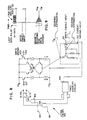
- FIG. 1 is a block diagram showing a magnetic recording system of the prior art.
- FIG. 2 is a schematic diagram showing circuit details of a WRITE DRIVER of the prior art.
- FIG. 3 is a timing diagram showing the interaction of inputs and outputs in a WRITE DRIVER of the prior art.
- FIG. 4 is a block diagram showing a magnetic recording system embodying the present invention.
- FIG. 5 is a schematic diagram showing circuit details of a WRITE DRIVER embodying the present invention.
- FIG. 5A and FIG. 5B show circuit details of current tapering circuits that may be incorporated into the WRITE DRIVER of FIG. 5.
- FIG. 6 is a timing diagram showing the interaction of inputs and outputs in a WRITE DRIVER embodying the present invention.
- FIG. 7 is a block diagram showing a magnetic recording system with an alternative embodiment of the present invention.
- FIG. 8 is a schematic diagram showing circuit details of a WRITE DRIVER with an alternative embodiment of the present invention.
- FIG. 9 is a timing diagram showing the interaction of inputs and outputs in a WRITE DRIVER with an alternative embodiment of the present invention.
- FIGs. 1 - 3 which illustrate in block diagram, schematic diagram, and timing diagram form respectively a typical prior art magnetic recording head and WRITE DRIVER, wherein the WRITE current at the completion of a WRITE cycle is abruptly terminated, resulting in adverse magnetic relaxation effects as described in the background of the invention.
- FIG. 4 illustrates in block diagram form a magnetic recording system embodying the present invention.
- the system comprises a magnetic recording head 140, a WRITE DRIVER 120, a current tapering circuit 100, and a READ AMPLIFIER 160.
- a typical data transfer sequence begins when external circuitry raises the WRITE ENABLE input 101 from logic state 0 to logic state 1.
- the current tapering circuit 100 passes the WRITE ENABLE input 101 with negligible delay to the WRITE DRIVER 120.
- external circuitry supplies logic levels representing binary data to the D+ and D- (121 and 122 respectively) inputs of the WRITE DRIVER 120.
- the WRITE DRIVER 120 translates the D+ and D- logic states into current pulses through the magnetic recording head 140.
- the current flowing through the magnetic recording head 140 creates a magnetic field which magnetizes the appropriate portion of a magnetic recording medium (not shown) adjacent to the magnetic recording head 140.
- the WRITE cycle then continues, with the WRITE ENABLE input 101 maintained at logic state 1 and the D+ and D- inputs toggling to create the appropriate magnetic recording head current and associated magnetic field, thus writing perhaps millions of bits of data to the magnetic storage medium.
- the current delivered from the WRITE DRIVER 120 to the magnetic recording head 140 likewise decays smoothly to 0 over the same time interval, which time interval, previously derived from measurement of the characteristic relaxation time of the domain walls in the magnetic recording head, results in greatly diminished Barkhausen noise, relaxation into a reproducible micro-magnetic domain state, and a final remanence state of zero.
- the data transfer sequence may also be complete, or alternatively it may continue in the form of a subsequent WRITE cycle or READ cycle.
- the data transfer sequence continues with external circuitry gating the READ AMP 160 data outputs to begin reading data from the magnetic storage medium as appropriate. Data integrity is assured throughout the READ cycle, since the adverse magnetic relaxation effects which would otherwise be generated by the magnetic recording head at the completion of the WRITE cycle have been corrected by the ramped termination of the WRITE DRIVER 120 current.
- the READ cycle is complete and the data transfer sequence may likewise be concluded. The entire process may then repeat itself by way of another data transfer sequence.
- FIGs. 5, 5A, and 5B illustrate in schematic diagram form a WRITE DRIVER embodying the present invention.
- the system comprises a WRITE DRIVER 120 with an embedded current tapering circuit including either a means for reducing the current in the magnetic recording head 140 according to an exponentially decaying function (e.g., an exponential taper circuit 105 as in FIG. 5B) or a means for reducing the current in the magnetic recording head according to a linear ramp function (e.g., a ramp taper circuit 112 as in FIG. 5A).
- an exponentially decaying function e.g., an exponential taper circuit 105 as in FIG. 5B
- a linear ramp function e.g., a ramp taper circuit 112 as in FIG. 5A
- a WRITE cycle begins when the WRITE ENABLE input 101 transitions from logic state 0 to logic state 1.
- the diode (114 or 107, respectively) begins conducting, rapidly charging the capacitor (116 or 110, respectively) and turning the transistor (113 or 106, respectively) ON.
- the WRITE DRIVER 120 is enabled, and the D+ and D- (121 and 122) inputs begin to control the WRITE current applied to the magnetic recording head 140.
- D+ is at logic 1 (and hence D- at logic 0)
- transistors 126 and 127 are ON, while transistors 136 and 137 are OFF.
- the WRITE current Iw flows through the magnetic recording head 140 from (-) to (+).
- transistors 136 and 137 are ON, while transistors 126 and 127 are OFF.
- the WRITE current Iw flows through the magnetic recording head 140 from (+) to (-).
- Transistors 125 and 135 are emitter followers biased by a constant rail current and as such they are always on. The output of each emitter follower tracks the input signal (D+ or D-, respectively), with an offset equal to the base emitter voltage.
- the WRITE ENABLE input 101 drops abruptly from logic state 1 to logic state 0 in response to an externally generated completion signal indicating completion of the WRITE operation.
- the diode 114 ceases to conduct.
- the capacitor 116 begins discharging through the constant current source 117.
- the voltage on the base of transistor 113 ramps linearly to 0 according to the time constant determined by the values of capacitor 116 and constant current source 117, which values are set to create a ramp reaching 0 potential at a time approximately equal to the characteristic relaxation time associated with the domain walls of the magnetic recording head 140 used in the WRITE DRIVER 120.
- the capacitor 116 connected to the base of transistor 113 discharges, the WRITE current Iw through transistor 113 likewise ramps linearly to 0, thereby providing controlled relaxation of the magnetic recording head 140.
- the completion of the WRITE cycle occurs in substantially the same manner as described above.
- the capacitor 110 discharges along a decaying exponential curve through resistor 109 according to a time constant determined so as to create an exponential function decaying to approximately 0 potential at a time approximately equal to the characteristic relaxation time associated with the domain walls of the magnetic recording head 140 used in the WRITE DRIVER 120.
- FIG. 6 illustrates in timing diagram form the interaction of inputs and outputs in a WRITE DRIVER embodying the present invention.
- the critical period of time with respect to magnetic relaxation occurs when the WRITE ENABLE transitions from logic state 1 to logic state 0.
- the current tapering circuit 100 of the present invention creates a smooth, elongated fall time to the WRITE current through the magnetic recording head 140.
- current is tapered according to either a linear ramp function or a decaying exponential function.
- FIGs. 7, 8, and 9 show respectively in block diagram, schematic diagram, and timing diagram form a magnetic recording system comprising an alternative embodiment of the present invention.
- this alternative embodiment includes a WRITE DRIVER 120 and a current tapering circuit 100 such as either of those described above in the preferred embodiments and illustrated in FIG 5A or FIG 5B.
- the alternative embodiment employs a timed enabling circuit 190 and a gating circuit 180.
- the final enabling circuit 190 is triggered by the negative-going transition of the WRITE ENABLE input 101 to provide an enabling signal to the gating circuit 180 for a predetermined period of time.
- the gating circuit provides a high frequency data termination burst signal on the D+ and D- inputs (121 and 122) to the WRITE DRIVER 120.
- FIG. 8 shows the particulars of the timed enabling circuit 190 and the gating circuit 180.
- the timed enabling circuit 190 (a monostable multivibrator, for instance) causes the gating circuit 180 to degate the data inputs 181 and 182 and gates the high frequency clock 183 to the D+ and D- inputs (121 and 122) of the WRITE DRIVER 120.
- the burst signal from the high frequency clock 183 is maintained on the D+ and D- inputs 121 and 122 for a period of time determined by the timed enabling circuit 190, which period is set such that the high frequency burst signal is gated to the WRITE DRIVER 120 during the same period of time the WRITE current Iw is ramping (or decaying) to 0.
- the timed enabling circuit 190 causes the gating circuit 180 to degate the high frequency clock 183 and regate the data input 181 to the D+ and D- inputs 121 and 122 of the WRITE DRIVER 120.
- the high frequency data termination burst signal coacts with the smooth ramp (or decaying exponential) of the current tapering circuit to provide a high frequency linearly (or exponentially) terminating WRITE current through the magnetic recording head.
- the timed enabling circuit 190 may be a monostable multivibrator, or, it may be a counter that counts the number of pulses in the burst signal and degates the high frequency clock after a given count is reached.
- the high frequency clock 183 may be replaced with a high frequency sinusoidal wave.
- either the high frequency clock or the high frequency sinusoidal wave may be replaced with a low frequency-to-high frequency square wave or sinusoidal wave. Any of these functions, in coaction with monotonically (i.e. linearly or exponentially) decaying taper circuit whose time constant is approximately as long as the characteristic relaxation time of the domain walls in the driven magnetic recording head, will provide a dramatic improvement in the adverse magnetic relaxation effects created by the magnetic recording head at WRITE cycle completion.
- the present invention is readily applicable to a wide variety of magnetic recording systems. For instance, it can be used in systems having ferrite inductive heads, in systems having thin film inductive heads, and in systems having thin film inductive-magnetoresistive in systems implementing single element READ/WRITE heads and in systems implementing dual element READ/WRITE heads.
- a system for controlling magnetic recording head relaxation in a magnetic recording system and to reduce READ/WRITE magnetic recording head noise following a WRITE cycle in a magnetic recording system.
- the system described allows a reproducible final micro-magnetic domain state following a WRITE cycle in a magnetic recording system and a final remanence state of zero in a magnetic recording head to be obtained.
Landscapes
- Digital Magnetic Recording (AREA)
Applications Claiming Priority (2)
| Application Number | Priority Date | Filing Date | Title |
|---|---|---|---|
| US07/517,783 US5168395A (en) | 1990-05-02 | 1990-05-02 | Controlled magnetic recording head relaxation in a magnetic recording system |
| US517783 | 1995-08-22 |
Publications (3)
| Publication Number | Publication Date |
|---|---|
| EP0455438A2 true EP0455438A2 (de) | 1991-11-06 |
| EP0455438A3 EP0455438A3 (en) | 1992-08-05 |
| EP0455438B1 EP0455438B1 (de) | 1996-07-03 |
Family
ID=24061212
Family Applications (1)
| Application Number | Title | Priority Date | Filing Date |
|---|---|---|---|
| EP91303831A Expired - Lifetime EP0455438B1 (de) | 1990-05-02 | 1991-04-26 | Magnetisches Aufzeichnungssystem |
Country Status (6)
| Country | Link |
|---|---|
| US (1) | US5168395A (de) |
| EP (1) | EP0455438B1 (de) |
| JP (1) | JPH04228103A (de) |
| KR (1) | KR960015919B1 (de) |
| DE (1) | DE69120600T2 (de) |
| TW (1) | TW316310B (de) |
Cited By (4)
| Publication number | Priority date | Publication date | Assignee | Title |
|---|---|---|---|---|
| EP0581705A1 (de) * | 1992-07-31 | 1994-02-02 | STMicroelectronics S.A. | Lese-/Schreibeumschaltvorrichtung des Kopfes eines Video-Aufzeichnungsgerätes |
| GB2308717A (en) * | 1995-12-27 | 1997-07-02 | Samsung Electronics Co Ltd | Magnetic head control circuit and method |
| WO2002025240A1 (en) * | 2000-09-21 | 2002-03-28 | Mts Systems Corporation | Multiple region convolver with tapering |
| EP1971921A4 (de) * | 2005-12-30 | 2009-07-15 | Texas Instruments Inc | Entmagnetisierung für einen schreibkopf |
Families Citing this family (34)
| Publication number | Priority date | Publication date | Assignee | Title |
|---|---|---|---|---|
| JP2857506B2 (ja) * | 1991-03-13 | 1999-02-17 | 株式会社日立製作所 | 磁気記録装置 |
| JPH0573817A (ja) * | 1991-06-24 | 1993-03-26 | Sony Corp | 磁気抵抗効果素子を有する磁気記録再生装置 |
| US5359470A (en) * | 1991-06-24 | 1994-10-25 | Sony Corporation | Magnetic recording/reproducing apparatus |
| US5455816A (en) * | 1992-05-18 | 1995-10-03 | At&T Global Information Solutions Company | MOS amplifier with gain control |
| US5323278A (en) * | 1992-09-17 | 1994-06-21 | International Business Machines Corporation | Low noise amplifier circuit for magnetoresistive sensors for fast read-write switching in low supply voltage applications |
| US5287231A (en) * | 1992-10-06 | 1994-02-15 | Vtc Inc. | Write circuit having current mirrors between predriver and write driver circuits for maximum head voltage swing |
| DE69316304T2 (de) * | 1992-10-09 | 1998-07-23 | Koninkl Philips Electronics Nv | Aufzeichnungsvorrichtung mit temperaturabhängiger Schreibstromsteuerung |
| JP2559966B2 (ja) * | 1993-03-08 | 1996-12-04 | インターナショナル・ビジネス・マシーンズ・コーポレイション | 磁気記録装置の読取り/書込み回路 |
| US5386328A (en) * | 1993-06-18 | 1995-01-31 | Silicon Systems, Inc. | Current mirror based write driver |
| JPH07134804A (ja) * | 1993-09-17 | 1995-05-23 | Fujitsu Ltd | 記録再生装置及び記録再生方法 |
| US5544135A (en) * | 1994-10-11 | 1996-08-06 | Quantum Corporation | Fault tolerant servo address mark for disk drive |
| US5696641A (en) * | 1995-05-10 | 1997-12-09 | Maxtor Corporation | Method using a biasing pattern on a magnetic storage media to reduce MR head noise |
| US6388476B1 (en) | 1995-06-07 | 2002-05-14 | Texas Instruments Incorporated | Self-switched cascode write driver |
| US5877911A (en) * | 1996-03-13 | 1999-03-02 | International Business Machines Corporation | Magneto-resistive head pre-amplifying circuit for avoiding output voltage transients |
| US5774505A (en) * | 1996-04-04 | 1998-06-30 | Hewlett-Packard Company | Intersymbol interference cancellation with reduced complexity |
| JP2923907B2 (ja) * | 1996-05-30 | 1999-07-26 | 日本電気株式会社 | 磁気ディスク装置 |
| KR100458753B1 (ko) * | 1996-12-05 | 2005-04-13 | 삼성전자주식회사 | 기록전류안정화회로 |
| US5994951A (en) * | 1997-01-21 | 1999-11-30 | Vtc Inc. | Automatic-tuning circuit for integrated continuous-time MOSFET-C filters |
| US6201653B1 (en) | 1998-06-12 | 2001-03-13 | International Business Machines Corporation | By-pass write drivers for high-performance data recording |
| US6252736B1 (en) * | 1998-12-28 | 2001-06-26 | Stmicroelectronics N.V. | System for preventing crosstalk noise in a disk drive |
| US6271978B1 (en) * | 1999-05-07 | 2001-08-07 | Texas Instruments Incorporated | Power efficient overshoot control for magnetic recording write driver |
| JP3522614B2 (ja) * | 1999-12-13 | 2004-04-26 | Tdk株式会社 | 薄膜磁気ヘッドの特性改善方法および装置 |
| US6724553B2 (en) * | 2001-03-26 | 2004-04-20 | Samsung Electronics Co., Ltd. | Method and apparatus for generating the optimum read timing for read and write offset of a magneto resistive head |
| JP2005222684A (ja) * | 2004-02-06 | 2005-08-18 | Agere Systems Inc | 書込みヘッド消磁方法および装置 |
| US7088537B2 (en) * | 2004-03-09 | 2006-08-08 | Seagate Technology Llc | Removing residual magnetization in a data transducer |
| US7092186B1 (en) | 2004-11-23 | 2006-08-15 | Western Digital Technologies, Inc. | Demagnetizing a head in a disk drive by increasing the frequency of an AC write signal while maintaining the write current amplitude |
| US7280294B2 (en) * | 2004-11-30 | 2007-10-09 | International Business Machines Corporation | Tri-state servowriter driver with slow return to zero |
| JP4250589B2 (ja) * | 2004-12-28 | 2009-04-08 | 株式会社東芝 | 記録ヘッドの残留磁化消磁機能を有するヘッドアンプ回路及び同回路を備えた磁気ディスク装置 |
| JP2006196107A (ja) * | 2005-01-14 | 2006-07-27 | Hitachi Global Storage Technologies Netherlands Bv | 磁気記録装置及び記録方法 |
| US7515371B1 (en) * | 2005-05-19 | 2009-04-07 | Maxtor Corporation | Channel postamble extension to de-gauss pole tips |
| US7280388B2 (en) * | 2005-12-07 | 2007-10-09 | Nahas Joseph J | MRAM with a write driver and method therefor |
| US7206223B1 (en) | 2005-12-07 | 2007-04-17 | Freescale Semiconductor, Inc. | MRAM memory with residual write field reset |
| US8310780B2 (en) | 2010-07-20 | 2012-11-13 | International Business Machines Corporation | Method and apparatus for bipolar servo marks writing with high output |
| US9978401B1 (en) | 2016-08-19 | 2018-05-22 | Seagate Technology Llc | Chirped current profile with undershoot feature |
Family Cites Families (14)
| Publication number | Priority date | Publication date | Assignee | Title |
|---|---|---|---|---|
| CH235672A (de) * | 1941-11-27 | 1944-12-15 | Licentia Gmbh | Verfahren zum magnetischen Aufzeichnen von durch Kombinationen einer Anzahl Elemente gebildeten Impulsfolgen. |
| US3009637A (en) * | 1959-10-30 | 1961-11-21 | Ibm | Locating end of file |
| US3618119A (en) * | 1970-03-13 | 1971-11-02 | Storage Technology Corp | Compensation in a magentic write circuit |
| JPS519417A (en) * | 1974-07-12 | 1976-01-26 | Fujitsu Ltd | Jikihetsudono shojihoshiki |
| JPS5465102A (en) * | 1977-11-04 | 1979-05-25 | Taiheiyo Eng | Treating of coal post for preservation of public in long wall type coal mining method |
| US4428008A (en) * | 1982-04-02 | 1984-01-24 | Ampex Corporation | Electronic switching circuit for use in magnetic head drives |
| JPS6047223A (ja) * | 1983-08-25 | 1985-03-14 | Sony Corp | 磁気抵抗効果型磁気ヘツド |
| JPH0610845B2 (ja) * | 1984-02-18 | 1994-02-09 | ティアツク株式会社 | デジタル磁気記録再生装置 |
| JPS6234308A (ja) * | 1985-08-07 | 1987-02-14 | Sankyo Seiki Mfg Co Ltd | デ−タ書き込み回路 |
| US4649447A (en) * | 1985-08-15 | 1987-03-10 | International Business Machines | Combed MR sensor |
| JPH0264903A (ja) * | 1988-08-30 | 1990-03-05 | Toshiba Corp | 磁気記録再生装置のデータ書込み回路 |
| US4970621A (en) * | 1988-09-09 | 1990-11-13 | Hewlett-Packard Company | Demagnetization of thin film magnetic recording transducers utilizing a decreasing AC current |
| JPH02158903A (ja) * | 1988-12-09 | 1990-06-19 | Mitsubishi Electric Corp | ヘッドドライバー |
| JPH02199604A (ja) * | 1989-01-30 | 1990-08-08 | Nec Corp | 磁気ディスク装置の書込み回路 |
-
1990
- 1990-05-02 US US07/517,783 patent/US5168395A/en not_active Expired - Lifetime
-
1991
- 1991-04-09 JP JP3103460A patent/JPH04228103A/ja active Pending
- 1991-04-26 EP EP91303831A patent/EP0455438B1/de not_active Expired - Lifetime
- 1991-04-26 KR KR1019910006747A patent/KR960015919B1/ko not_active Expired - Fee Related
- 1991-04-26 DE DE69120600T patent/DE69120600T2/de not_active Expired - Fee Related
-
1992
- 1992-01-31 TW TW081100828A patent/TW316310B/zh active
Cited By (9)
| Publication number | Priority date | Publication date | Assignee | Title |
|---|---|---|---|---|
| EP0581705A1 (de) * | 1992-07-31 | 1994-02-02 | STMicroelectronics S.A. | Lese-/Schreibeumschaltvorrichtung des Kopfes eines Video-Aufzeichnungsgerätes |
| FR2694469A1 (fr) * | 1992-07-31 | 1994-02-04 | Sgs Thomson Microelectronics | Dispositif de commutation écriture/lecture d'une tête de magnétoscope. |
| US5724201A (en) * | 1992-07-31 | 1998-03-03 | Sgs-Thomson Microelectronics S.A. | Method and apparatus for reducing transition time for a magnetic head to switch from a write made to a read mode by reducing a maximum current value at different rates |
| GB2308717A (en) * | 1995-12-27 | 1997-07-02 | Samsung Electronics Co Ltd | Magnetic head control circuit and method |
| DE19642375A1 (de) * | 1995-12-27 | 1997-07-03 | Samsung Electronics Co Ltd | Schaltkreis zum Steuern der Schreibströme eines Magnetplattenaufzeichnungsgeräts und Verfahren dazu |
| US5910861A (en) * | 1995-12-27 | 1999-06-08 | Samsung Electronics Co., Ltd. | Technique for controlling the write currents of a magnetic disk recording apparatus |
| WO2002025240A1 (en) * | 2000-09-21 | 2002-03-28 | Mts Systems Corporation | Multiple region convolver with tapering |
| US7062357B2 (en) | 2000-09-21 | 2006-06-13 | Mts Systems Corporation | Multiple region convolver with tapering |
| EP1971921A4 (de) * | 2005-12-30 | 2009-07-15 | Texas Instruments Inc | Entmagnetisierung für einen schreibkopf |
Also Published As
| Publication number | Publication date |
|---|---|
| US5168395A (en) | 1992-12-01 |
| EP0455438A3 (en) | 1992-08-05 |
| JPH04228103A (ja) | 1992-08-18 |
| DE69120600D1 (de) | 1996-08-08 |
| EP0455438B1 (de) | 1996-07-03 |
| KR960015919B1 (ko) | 1996-11-23 |
| DE69120600T2 (de) | 1997-01-23 |
| KR910020647A (ko) | 1991-12-20 |
| TW316310B (de) | 1997-09-21 |
Similar Documents
| Publication | Publication Date | Title |
|---|---|---|
| EP0455438B1 (de) | Magnetisches Aufzeichnungssystem | |
| US4970621A (en) | Demagnetization of thin film magnetic recording transducers utilizing a decreasing AC current | |
| US8260568B2 (en) | Moving direction detector | |
| US5780828A (en) | Interactive video systems | |
| US3252099A (en) | Waveform shaping system for slimming filter control and symmetrizing | |
| EP0027547B1 (de) | Gerät zur Datensignal-Detektion | |
| JPH04500285A (ja) | 磁気光学メモリに記録するために磁界を変調するための制御回路 | |
| US10095263B1 (en) | Apparatus and method for calibrating signal synchronization | |
| US6175319B1 (en) | Power-tailored write-current method | |
| US6952316B2 (en) | Open head detection circuit and method in a voltage or current mode driver | |
| EP0325491B1 (de) | Vorrichtung zur automatischen Verstärkungskontrolle in einem optischen Speichergerät | |
| US7515371B1 (en) | Channel postamble extension to de-gauss pole tips | |
| CN87107898A (zh) | 缩减光检波器的存储效应的装置和方法 | |
| EP0203786A2 (de) | Drehzahlregelungsgerät für Aufzeichnungsträger | |
| EP0555865B1 (de) | Servospurfolgekreis für Gerät für optische Scheiben | |
| JP2556574B2 (ja) | 光メモリ装置 | |
| US3526901A (en) | Nrz digital magnetic recording | |
| US4177521A (en) | Output timing arrangement for single-wall magnetic domain apparatus | |
| US3668665A (en) | Apparatus for ensuring timing track accuracy | |
| JPS597157B2 (ja) | 磁気バブル装置の試験方法 | |
| RU2038693C1 (ru) | Троичный триггер | |
| SU1695411A1 (ru) | Устройство дл контрол времени срабатывани электромагнитного механизма | |
| KR910006630Y1 (ko) | 광자기 디스크장치의 실시간 기록 검증회로 | |
| JP2518931B2 (ja) | フロッピ―ディスク装置の書込回路 | |
| US3934235A (en) | Reactive coupled drive circuit for magnetic bubble memories |
Legal Events
| Date | Code | Title | Description |
|---|---|---|---|
| PUAI | Public reference made under article 153(3) epc to a published international application that has entered the european phase |
Free format text: ORIGINAL CODE: 0009012 |
|
| AK | Designated contracting states |
Kind code of ref document: A2 Designated state(s): DE FR GB |
|
| 17P | Request for examination filed |
Effective date: 19911219 |
|
| PUAL | Search report despatched |
Free format text: ORIGINAL CODE: 0009013 |
|
| AK | Designated contracting states |
Kind code of ref document: A3 Designated state(s): DE FR GB |
|
| 17Q | First examination report despatched |
Effective date: 19940912 |
|
| GRAH | Despatch of communication of intention to grant a patent |
Free format text: ORIGINAL CODE: EPIDOS IGRA |
|
| GRAH | Despatch of communication of intention to grant a patent |
Free format text: ORIGINAL CODE: EPIDOS IGRA |
|
| GRAA | (expected) grant |
Free format text: ORIGINAL CODE: 0009210 |
|
| AK | Designated contracting states |
Kind code of ref document: B1 Designated state(s): DE FR GB |
|
| REF | Corresponds to: |
Ref document number: 69120600 Country of ref document: DE Date of ref document: 19960808 |
|
| ET | Fr: translation filed | ||
| PGFP | Annual fee paid to national office [announced via postgrant information from national office to epo] |
Ref country code: DE Payment date: 19970422 Year of fee payment: 7 |
|
| PLBE | No opposition filed within time limit |
Free format text: ORIGINAL CODE: 0009261 |
|
| STAA | Information on the status of an ep patent application or granted ep patent |
Free format text: STATUS: NO OPPOSITION FILED WITHIN TIME LIMIT |
|
| 26N | No opposition filed | ||
| PG25 | Lapsed in a contracting state [announced via postgrant information from national office to epo] |
Ref country code: FR Free format text: LAPSE BECAUSE OF NON-PAYMENT OF DUE FEES Effective date: 19971231 |
|
| REG | Reference to a national code |
Ref country code: FR Ref legal event code: ST |
|
| PG25 | Lapsed in a contracting state [announced via postgrant information from national office to epo] |
Ref country code: DE Free format text: LAPSE BECAUSE OF NON-PAYMENT OF DUE FEES Effective date: 19990202 |
|
| PGFP | Annual fee paid to national office [announced via postgrant information from national office to epo] |
Ref country code: GB Payment date: 19990330 Year of fee payment: 9 |
|
| PG25 | Lapsed in a contracting state [announced via postgrant information from national office to epo] |
Ref country code: GB Free format text: LAPSE BECAUSE OF NON-PAYMENT OF DUE FEES Effective date: 20000426 |
|
| GBPC | Gb: european patent ceased through non-payment of renewal fee |
Effective date: 20000426 |