EP0455483A2 - Schwache parasitische FET-Topologie für leistungs- und Niedrig-Rauschfaktor-GaAs-FET - Google Patents
Schwache parasitische FET-Topologie für leistungs- und Niedrig-Rauschfaktor-GaAs-FET Download PDFInfo
- Publication number
- EP0455483A2 EP0455483A2 EP91303962A EP91303962A EP0455483A2 EP 0455483 A2 EP0455483 A2 EP 0455483A2 EP 91303962 A EP91303962 A EP 91303962A EP 91303962 A EP91303962 A EP 91303962A EP 0455483 A2 EP0455483 A2 EP 0455483A2
- Authority
- EP
- European Patent Office
- Prior art keywords
- source
- gate
- contacts
- pad
- drain
- Prior art date
- Legal status (The legal status is an assumption and is not a legal conclusion. Google has not performed a legal analysis and makes no representation as to the accuracy of the status listed.)
- Granted
Links
- 229910001218 Gallium arsenide Inorganic materials 0.000 title claims abstract description 12
- 230000003071 parasitic effect Effects 0.000 title description 11
- JBRZTFJDHDCESZ-UHFFFAOYSA-N AsGa Chemical compound [As]#[Ga] JBRZTFJDHDCESZ-UHFFFAOYSA-N 0.000 claims abstract description 11
- 239000000758 substrate Substances 0.000 claims description 19
- 239000010931 gold Substances 0.000 claims description 7
- 239000004020 conductor Substances 0.000 claims description 6
- PCHJSUWPFVWCPO-UHFFFAOYSA-N gold Chemical compound [Au] PCHJSUWPFVWCPO-UHFFFAOYSA-N 0.000 claims description 5
- 229910052737 gold Inorganic materials 0.000 claims description 5
- BASFCYQUMIYNBI-UHFFFAOYSA-N platinum Chemical compound [Pt] BASFCYQUMIYNBI-UHFFFAOYSA-N 0.000 claims description 5
- BYDQGSVXQDOSJJ-UHFFFAOYSA-N [Ge].[Au] Chemical compound [Ge].[Au] BYDQGSVXQDOSJJ-UHFFFAOYSA-N 0.000 claims description 4
- 239000010936 titanium Substances 0.000 claims description 4
- RTAQQCXQSZGOHL-UHFFFAOYSA-N Titanium Chemical compound [Ti] RTAQQCXQSZGOHL-UHFFFAOYSA-N 0.000 claims description 3
- 229910052719 titanium Inorganic materials 0.000 claims description 3
- 229910000927 Ge alloy Inorganic materials 0.000 claims description 2
- 229910052697 platinum Inorganic materials 0.000 claims description 2
- 230000008878 coupling Effects 0.000 claims 1
- 238000010168 coupling process Methods 0.000 claims 1
- 238000005859 coupling reaction Methods 0.000 claims 1
- 239000000463 material Substances 0.000 claims 1
- 239000004065 semiconductor Substances 0.000 claims 1
- 230000010355 oscillation Effects 0.000 description 5
- 241000239290 Araneae Species 0.000 description 3
- 238000012986 modification Methods 0.000 description 3
- 230000004048 modification Effects 0.000 description 3
- 230000009467 reduction Effects 0.000 description 3
- 229910045601 alloy Inorganic materials 0.000 description 2
- 239000000956 alloy Substances 0.000 description 2
- 238000010276 construction Methods 0.000 description 2
- 238000001465 metallisation Methods 0.000 description 2
- 230000004888 barrier function Effects 0.000 description 1
- 230000008859 change Effects 0.000 description 1
- 230000001419 dependent effect Effects 0.000 description 1
- 230000000694 effects Effects 0.000 description 1
- 230000005669 field effect Effects 0.000 description 1
- 238000002513 implantation Methods 0.000 description 1
- 238000002955 isolation Methods 0.000 description 1
- 229910052710 silicon Inorganic materials 0.000 description 1
- 239000010703 silicon Substances 0.000 description 1
- 238000010561 standard procedure Methods 0.000 description 1
Images


Classifications
-
- H—ELECTRICITY
- H10—SEMICONDUCTOR DEVICES; ELECTRIC SOLID-STATE DEVICES NOT OTHERWISE PROVIDED FOR
- H10D—INORGANIC ELECTRIC SEMICONDUCTOR DEVICES
- H10D64/00—Electrodes of devices having potential barriers
- H10D64/20—Electrodes characterised by their shapes, relative sizes or dispositions
- H10D64/27—Electrodes not carrying the current to be rectified, amplified, oscillated or switched, e.g. gates
- H10D64/311—Gate electrodes for field-effect devices
- H10D64/411—Gate electrodes for field-effect devices for FETs
Definitions
- This invention relates to field effect transistors (FETs) and, more specifically, to power and low noise FETs.
- Gallium Arsenide (GaAs) FETs are generally formed by providing a substrate of semi-insulating GaAs having a doped region at a surface region thereof with metallization on the doped surface region which makes an ohmic contact with the doped region to form source and drain regions and further metallization on the doped surface region which forms a Schottky barrier diode with the doped region to form the gate region, the channel extending between the source and drain in the doped region of the substrate and under the gate.
- GaAs Gallium Arsenide
- the layout topology of the FET and its effect on device performance is an area that is very weakly addressed in the literature.
- the interdigitated and pi gate feed structures have been industry standards for the last ten years with only minor modifications.
- the interdigitated FET has served well in low noise and power applications where a large gate periphery is required in a compact form.
- the pi FET has typically served in low noise designs where a small gate periphery is desired.
- the source is formed as many separate spaced apart segments with the gate being a thin line between the source segments and drain, the gate also including fingers extending therefrom between the source segment.
- both the source and drain are formed as many separate spaced apart segments, the source and drain segments being interleaved or alternating and the gate being a thin line having fingers which extend between each opposing pair of source and drain elements.
- Both of these topologies limit the size of the FET periphery on MMIC chips and have parasitic components that increase the noise figure and limit the high frequency performance of the FET.
- the spider FET allows more FET area on the MMIC chip and allows the parasitics to be minimized by its topology.
- GaAs FET which overcomes or minimizes the above noted problems of the prior art. This is accomplished by providing a substantial change in the topology of the source, gate and drain regions over the doped region of the substratre.
- a semi-insulating GaAs substrate having a doped region at a surface thereof.
- a central gate pad preferably of layers of titanium, platinum and gold (Ti/Pt/Au) in that order, having a plurality of fingers extending therefrom is disposed over the doped region and forms a Schottky diode therewith.
- On opposing sides of said gate pad and over the doped region are disposed alternate source and drain regions with the fingers from the central gate pad extending between each adjacent source and drain pair.
- the source regions on one side of the gate pad region are coupled to a first source pad and the source regions on the other side of the gate pad region are coupled to a second source pad.
- the drain regions are all coupled to a drain pad, preferably via a air bridge over the source regions.
- the source and drain pads can be over the doped region, but need not be.
- the source and drain pads and regions make an ohmic contact with the substrate thereunder and are preferably a gold-germanium (Au-Ge) alloy.
- the gate fingers are preferably offset toward the source.
- the source pads optionally include a via therein extending to the underside of the substrate and having a conductor, preferbly of gold (Au) extending from the source pad along the via to the backside of the substrate for connecting the source pad to a ground plane, connecting plural source pads together or for connection to other circuitry at or by way of the underside of the substrate.
- Au gold
- the FET topology of the present invention achieves lower minimum noise figure (Fmins) in a more compact structure than either the pi-gate or interdigitated FETs and provides many more gate feeds than are available with the prior art topologies without increasing the gate pad area to reduce gate resistance.
- the improved FET performance in accordance with the present invention is achieved by reducing the gate feed resistance and minimizing the parasitic gate to source capacitance in the region of the gate feed.
- the gate bond pad of the FET also contributes to parasitic gate capacitance and, for the FET in accordance with the present invention, is of minimum producible dimensions.
- the FET topology in accordance with the present invention also makes effective use of the gate bond bad by combining it with the gate feeds. This allows the gate feeds to be plated to reduce gate feed resistance.
- the combination of the drain regions, drain air bridges and drain pad form a "U-shaped" stub wherein oscillations can be set up at certain frequencies, depending upon dimensions and other conditions. These oscillations may be undesirable and can be eliminated by providing a conductive strap across the open end of the "U".
- the above described topology allows larger devices to be implemented in substantially the same area.
- the gate feed structure incorporates the gate pad to minimize parasitics.
- the topology of the subject invention reduces the gate rsistance by offering a plated gate feed and a large number of gate feeds, while minimizing the parasitics. These advantages are achieved by an increase in the output capacitance (Cds).
- the source to gate capacitance does not directly affect the noise figure of the FET.
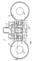
- FIGURES 1 and 2 there is shown a first embodiment of a GaAs FET structure in accordance with the present invention.
- the structure includes a semi-insulating GaAs substrate 1 having a surface region 3 which is doped N-type, preferably with silicon.
- a source pad 5 of electrically conductive material, preferably a gold-germanium (Au-Ge) alloy, which makes ohmic contact with the doped region 3 is disposed over a portion of the region 3 and includes an aperture 6 therein which conforms with a via 7 in and extending through the substrate.
- Au-Ge gold-germanium
- a plurality of source regions 11 identical to the source pad 5 in construction extend from the source pad and are spaced apart.
- a drain pad 13 of electrically conductive material, preferably the same gold-germanium alloy as used to form the source pad 5, which makes ohmic contact with the doped region 3 is disposed over a portion of the region 3 spaced from the source pad 5.
- a plurality of drain regions 15 identical to the drain pad 13 in construction are interleaved between the source regions 11 and are coupled to the drain pad 13 via an air bridge 17.
- identical source and drain structures are provided on opposite sides of the gate pad 19, the structure being symmetrical relative to a line drawn through the center of the gate pad and the drain pad.
- the gate pad 19 is formed of electrically conductive material, preferably plural layers of titanium and gold in that order from the substrate 1.
- a plurality of electrically conductive fingers 21 are coupled to the gate pad 19 and extend between each opposing pair of a source region 11 and a drain region 15. It can be seen that the structure of the gate pad 19 with its fingers 21 takes the shape of a spider or the like.
- drain pad 13, drain regions 15 and air bridge 17 form a U-shaped structure.
- This physical arrangements can cause oscillations at high frequencies, the particular frequency of oscillation being dependent upon various physical factors which are well known. In the event these oscillations become undesirable, they are eliminated or minimized by providing a strap 23 which couples together the two remote drain regions 15 at the far ends of the "U" to provide a continuous electrically conductive loop.
- FIGURE 3 there is shown a second embodiment of the present invention which is a power FET and wherein like numbers represent the same or similar structure to that of FIGURES 1 and 2.
- a pair of source pads 5 having source regions 11 extending therefrom and a drain pad 13 having a portion 25 thereof extending between the two rows of source regions.
- the drain regions 15 extend from the drain portion 25 and are interleaved between the source regions 11.
- Two gate pads 19 are provided for providing two different gate structures. It should be understood that the gate pads 19 could be coupled together or be provided as a single gate pad, if appropriate.
- a plurality of gate fingers 21 are positioned between opposing source regions 11 and drain regions 15 as in the embodiment of FIGURES 1 and 2. However, in this embodiment, the source regions 11 are coupled together and to the source pad 5 via an air bridge 27.
- FIGURE 4 there is shown a third embodiment in accordance with the present invention.
- This embodiment is identical to the embodiment of FIGURES 1 and 2 except that each of the source pads 5 except the two end source pads 5a of the structure is coupled to source regions 11 on both opposing sides thereof as shown in source region 5b with one via 7 in each of the source pads.
- the drain pad 13a is elongated so that it can be coupled to drain regions 15 at two or more banks 29 of drain regions wherein a bank is defined as one grouping of gate, source and drain components between an adjacent pair of vias as seen in FIGURE 4. It is also apparent that there can be plural gate pads 19, one for each bank 29 or the gate pad could be elongated in the same manner as the drain pad 13a to provide an interconnected gate structure.
Landscapes
- Junction Field-Effect Transistors (AREA)
Applications Claiming Priority (2)
| Application Number | Priority Date | Filing Date | Title |
|---|---|---|---|
| US07/518,349 US5023677A (en) | 1990-05-02 | 1990-05-02 | Low parasitic FET topology for power and low noise GaAs FETs |
| US518349 | 1990-05-02 |
Publications (3)
| Publication Number | Publication Date |
|---|---|
| EP0455483A2 true EP0455483A2 (de) | 1991-11-06 |
| EP0455483A3 EP0455483A3 (en) | 1993-06-30 |
| EP0455483B1 EP0455483B1 (de) | 2002-03-27 |
Family
ID=24063550
Family Applications (1)
| Application Number | Title | Priority Date | Filing Date |
|---|---|---|---|
| EP91303962A Expired - Lifetime EP0455483B1 (de) | 1990-05-02 | 1991-05-01 | Schwach parasitäre FET-Topologie für Leistungs- und Niedrig-Rauschfaktor-GaAs-FET |
Country Status (5)
| Country | Link |
|---|---|
| US (1) | US5023677A (de) |
| EP (1) | EP0455483B1 (de) |
| JP (1) | JPH04229629A (de) |
| KR (1) | KR910020922A (de) |
| DE (1) | DE69132966T2 (de) |
Cited By (3)
| Publication number | Priority date | Publication date | Assignee | Title |
|---|---|---|---|---|
| EP0494625A1 (de) * | 1991-01-10 | 1992-07-15 | Fujitsu Limited | Halbleiteranordnung zur Verbesserung der Hochfrequenzcharakteristiken und zur Vermeidung von Rissen im Chip |
| EP0862224A1 (de) * | 1997-02-28 | 1998-09-02 | Nec Corporation | Halbleiteranordnung |
| GB2444159B (en) * | 2006-11-22 | 2011-04-20 | Filtronic Compound Semiconductors Ltd | A multigate schottky diode |
Families Citing this family (14)
| Publication number | Priority date | Publication date | Assignee | Title |
|---|---|---|---|---|
| JP2557561B2 (ja) * | 1990-10-09 | 1996-11-27 | 三菱電機株式会社 | 半導体装置 |
| JPH04171734A (ja) * | 1990-11-02 | 1992-06-18 | Mitsubishi Electric Corp | 半導体装置 |
| JP2758531B2 (ja) * | 1992-04-22 | 1998-05-28 | 三菱電機株式会社 | 半導体装置 |
| US5659267A (en) * | 1995-11-03 | 1997-08-19 | Motorola, Inc. | High gain K-band power amplifier with unconditionally stable MMIC FET cells |
| US5734189A (en) * | 1996-12-09 | 1998-03-31 | Itt Industries, Inc. | Low parasitic source inductance field-effect transistor device having via connections disposed along an outer periphery thereof |
| JP3499103B2 (ja) * | 1997-02-21 | 2004-02-23 | 三菱電機株式会社 | 半導体装置 |
| US6081006A (en) * | 1998-08-13 | 2000-06-27 | Cisco Systems, Inc. | Reduced size field effect transistor |
| JP2000138236A (ja) | 1998-08-26 | 2000-05-16 | Mitsubishi Electric Corp | 半導体装置 |
| WO2002025810A2 (en) | 2000-09-22 | 2002-03-28 | U.S. Monolithics, L.L.C. | Mmic folded power amplifier |
| US6362689B1 (en) | 2000-09-22 | 2002-03-26 | U.S. Monolithics, L.L.C. | MMIC folded power amplifier |
| US6664855B2 (en) * | 2001-06-04 | 2003-12-16 | U.S. Monolithics, L.L.C. | MMIC driver amplifier having zig-zag RF signal flow |
| US6545543B2 (en) | 2001-07-06 | 2003-04-08 | Remec, Inc. | Small aspect ratio MMIC power amplifier layout |
| US6774416B2 (en) * | 2001-07-16 | 2004-08-10 | Nanowave, Inc | Small area cascode FET structure operating at mm-wave frequencies |
| US10629526B1 (en) * | 2018-10-11 | 2020-04-21 | Nxp Usa, Inc. | Transistor with non-circular via connections in two orientations |
Family Cites Families (5)
| Publication number | Priority date | Publication date | Assignee | Title |
|---|---|---|---|---|
| US3969745A (en) * | 1974-09-18 | 1976-07-13 | Texas Instruments Incorporated | Interconnection in multi element planar structures |
| JPS55108775A (en) * | 1979-02-09 | 1980-08-21 | Fujitsu Ltd | Semiconductor device |
| JPS6163062A (ja) * | 1984-09-03 | 1986-04-01 | Sanyo Electric Co Ltd | 電界効果トランジスタ |
| DE3504662A1 (de) * | 1985-02-12 | 1986-08-14 | ANT Nachrichtentechnik GmbH, 7150 Backnang | In eine wellenleitung eingefuegtes halbleiterbauelement |
| US4935805A (en) * | 1988-05-16 | 1990-06-19 | Eaton Corporation | T-type undercut electrical contact on a semiconductor substrate |
-
1990
- 1990-05-02 US US07/518,349 patent/US5023677A/en not_active Expired - Lifetime
-
1991
- 1991-05-01 JP JP3100140A patent/JPH04229629A/ja active Pending
- 1991-05-01 KR KR1019910007044A patent/KR910020922A/ko not_active Withdrawn
- 1991-05-01 DE DE69132966T patent/DE69132966T2/de not_active Expired - Fee Related
- 1991-05-01 EP EP91303962A patent/EP0455483B1/de not_active Expired - Lifetime
Cited By (6)
| Publication number | Priority date | Publication date | Assignee | Title |
|---|---|---|---|---|
| EP0494625A1 (de) * | 1991-01-10 | 1992-07-15 | Fujitsu Limited | Halbleiteranordnung zur Verbesserung der Hochfrequenzcharakteristiken und zur Vermeidung von Rissen im Chip |
| US5287072A (en) * | 1991-01-10 | 1994-02-15 | Fujitsu Limited | Semiconductor device for improving high-frequency characteristics and avoiding chip cracking |
| EP0862224A1 (de) * | 1997-02-28 | 1998-09-02 | Nec Corporation | Halbleiteranordnung |
| KR100292904B1 (ko) * | 1997-02-28 | 2001-07-12 | 가네꼬 히사시 | 반도체장치 |
| CN1123933C (zh) * | 1997-02-28 | 2003-10-08 | Nec化合物半导体器件株式会社 | 半导体器件 |
| GB2444159B (en) * | 2006-11-22 | 2011-04-20 | Filtronic Compound Semiconductors Ltd | A multigate schottky diode |
Also Published As
| Publication number | Publication date |
|---|---|
| EP0455483B1 (de) | 2002-03-27 |
| DE69132966D1 (de) | 2002-05-02 |
| JPH04229629A (ja) | 1992-08-19 |
| US5023677A (en) | 1991-06-11 |
| DE69132966T2 (de) | 2002-10-17 |
| EP0455483A3 (en) | 1993-06-30 |
| KR910020922A (ko) | 1991-12-20 |
Similar Documents
| Publication | Publication Date | Title |
|---|---|---|
| US5023677A (en) | Low parasitic FET topology for power and low noise GaAs FETs | |
| KR102586156B1 (ko) | 내부-급전 핑거들을 갖는 고전력 트랜지스터 | |
| US8169008B2 (en) | Semiconductor device | |
| US5025296A (en) | Center tapped FET | |
| US6081006A (en) | Reduced size field effect transistor | |
| US4359754A (en) | Semiconductor device | |
| US4298879A (en) | Field effect transistor | |
| US4298846A (en) | Semiconductor device | |
| JP2004039657A (ja) | 半導体装置 | |
| US6891267B2 (en) | Semiconductor switching circuit device | |
| US4549197A (en) | Common-gate GaAs FET design for monolithic microwave integrated circuits | |
| US6313512B1 (en) | Low source inductance compact FET topology for power amplifiers | |
| CN116420217B (zh) | 晶体管 | |
| JP3185441B2 (ja) | 高周波高出力電界効果トランジスタ | |
| US12599008B2 (en) | Transistor with source manifold in non-active die region | |
| JP2679781B2 (ja) | 半導体装置 | |
| JPH05335487A (ja) | 伝送回路素子 | |
| US6297700B1 (en) | RF power transistor having cascaded cells with phase matching between cells | |
| JPS6228788Y2 (de) | ||
| JP2000101067A (ja) | 半導体装置および集積回路装置 | |
| US4786881A (en) | Amplifier with integrated feedback network | |
| JPH11265983A (ja) | 半導体装置 | |
| JPH07226489A (ja) | マイクロ波半導体装置 | |
| JPH065636A (ja) | マイクロ波半導体装置 | |
| JP3468851B2 (ja) | モノリシックマイクロ波ic |
Legal Events
| Date | Code | Title | Description |
|---|---|---|---|
| PUAI | Public reference made under article 153(3) epc to a published international application that has entered the european phase |
Free format text: ORIGINAL CODE: 0009012 |
|
| AK | Designated contracting states |
Kind code of ref document: A2 Designated state(s): DE FR GB IT NL |
|
| PUAL | Search report despatched |
Free format text: ORIGINAL CODE: 0009013 |
|
| AK | Designated contracting states |
Kind code of ref document: A3 Designated state(s): DE FR GB IT NL |
|
| 17P | Request for examination filed |
Effective date: 19931221 |
|
| 17Q | First examination report despatched |
Effective date: 19950309 |
|
| RIC1 | Information provided on ipc code assigned before grant |
Free format text: 7H 01L 29/417 A, 7H 01L 29/812 B |
|
| GRAG | Despatch of communication of intention to grant |
Free format text: ORIGINAL CODE: EPIDOS AGRA |
|
| GRAG | Despatch of communication of intention to grant |
Free format text: ORIGINAL CODE: EPIDOS AGRA |
|
| GRAH | Despatch of communication of intention to grant a patent |
Free format text: ORIGINAL CODE: EPIDOS IGRA |
|
| REG | Reference to a national code |
Ref country code: GB Ref legal event code: IF02 |
|
| GRAH | Despatch of communication of intention to grant a patent |
Free format text: ORIGINAL CODE: EPIDOS IGRA |
|
| GRAA | (expected) grant |
Free format text: ORIGINAL CODE: 0009210 |
|
| AK | Designated contracting states |
Kind code of ref document: B1 Designated state(s): DE FR GB IT NL |
|
| PG25 | Lapsed in a contracting state [announced via postgrant information from national office to epo] |
Ref country code: IT Free format text: LAPSE BECAUSE OF FAILURE TO SUBMIT A TRANSLATION OF THE DESCRIPTION OR TO PAY THE FEE WITHIN THE PRESCRIBED TIME-LIMIT;WARNING: LAPSES OF ITALIAN PATENTS WITH EFFECTIVE DATE BEFORE 2007 MAY HAVE OCCURRED AT ANY TIME BEFORE 2007. THE CORRECT EFFECTIVE DATE MAY BE DIFFERENT FROM THE ONE RECORDED. Effective date: 20020327 |
|
| REF | Corresponds to: |
Ref document number: 69132966 Country of ref document: DE Date of ref document: 20020502 |
|
| ET | Fr: translation filed | ||
| PLBE | No opposition filed within time limit |
Free format text: ORIGINAL CODE: 0009261 |
|
| STAA | Information on the status of an ep patent application or granted ep patent |
Free format text: STATUS: NO OPPOSITION FILED WITHIN TIME LIMIT |
|
| 26N | No opposition filed |
Effective date: 20021230 |
|
| PGFP | Annual fee paid to national office [announced via postgrant information from national office to epo] |
Ref country code: NL Payment date: 20040413 Year of fee payment: 14 |
|
| PGFP | Annual fee paid to national office [announced via postgrant information from national office to epo] |
Ref country code: DE Payment date: 20040528 Year of fee payment: 14 |
|
| PG25 | Lapsed in a contracting state [announced via postgrant information from national office to epo] |
Ref country code: NL Free format text: LAPSE BECAUSE OF NON-PAYMENT OF DUE FEES Effective date: 20051201 Ref country code: DE Free format text: LAPSE BECAUSE OF NON-PAYMENT OF DUE FEES Effective date: 20051201 |
|
| NLV4 | Nl: lapsed or anulled due to non-payment of the annual fee |
Effective date: 20051201 |
|
| PGFP | Annual fee paid to national office [announced via postgrant information from national office to epo] |
Ref country code: GB Payment date: 20070410 Year of fee payment: 17 |
|
| PGFP | Annual fee paid to national office [announced via postgrant information from national office to epo] |
Ref country code: FR Payment date: 20070503 Year of fee payment: 17 |
|
| GBPC | Gb: european patent ceased through non-payment of renewal fee |
Effective date: 20080501 |
|
| REG | Reference to a national code |
Ref country code: FR Ref legal event code: ST Effective date: 20090119 |
|
| PG25 | Lapsed in a contracting state [announced via postgrant information from national office to epo] |
Ref country code: FR Free format text: LAPSE BECAUSE OF NON-PAYMENT OF DUE FEES Effective date: 20080602 |
|
| PG25 | Lapsed in a contracting state [announced via postgrant information from national office to epo] |
Ref country code: GB Free format text: LAPSE BECAUSE OF NON-PAYMENT OF DUE FEES Effective date: 20080501 |