EP0455857A1 - Appareil et procédés améliorés d'inspection de surface et de mesure des distortions de manière rétroréflective - Google Patents
Appareil et procédés améliorés d'inspection de surface et de mesure des distortions de manière rétroréflective Download PDFInfo
- Publication number
- EP0455857A1 EP0455857A1 EP90108857A EP90108857A EP0455857A1 EP 0455857 A1 EP0455857 A1 EP 0455857A1 EP 90108857 A EP90108857 A EP 90108857A EP 90108857 A EP90108857 A EP 90108857A EP 0455857 A1 EP0455857 A1 EP 0455857A1
- Authority
- EP
- European Patent Office
- Prior art keywords
- light
- image
- elements
- retroreflective
- test
- Prior art date
- Legal status (The legal status is an assumption and is not a legal conclusion. Google has not performed a legal analysis and makes no representation as to the accuracy of the status listed.)
- Withdrawn
Links
- 238000000034 method Methods 0.000 title claims abstract description 24
- 238000007689 inspection Methods 0.000 title description 4
- 238000005259 measurement Methods 0.000 title description 3
- 238000005286 illumination Methods 0.000 claims abstract description 13
- 230000035945 sensitivity Effects 0.000 claims abstract description 9
- 230000003287 optical effect Effects 0.000 claims description 10
- 230000008859 change Effects 0.000 claims description 4
- 238000004519 manufacturing process Methods 0.000 claims description 2
- 230000002730 additional effect Effects 0.000 claims 1
- 238000003384 imaging method Methods 0.000 claims 1
- 230000007547 defect Effects 0.000 description 36
- 230000000694 effects Effects 0.000 description 16
- 239000011324 bead Substances 0.000 description 4
- 239000006185 dispersion Substances 0.000 description 4
- 239000002184 metal Substances 0.000 description 4
- 239000011521 glass Substances 0.000 description 3
- 108020003564 Retroelements Proteins 0.000 description 2
- 230000009471 action Effects 0.000 description 2
- 230000008901 benefit Effects 0.000 description 2
- 238000010276 construction Methods 0.000 description 2
- 238000006073 displacement reaction Methods 0.000 description 2
- 230000005855 radiation Effects 0.000 description 2
- JEYCTXHKTXCGPB-UHFFFAOYSA-N Methaqualone Chemical compound CC1=CC=CC=C1N1C(=O)C2=CC=CC=C2N=C1C JEYCTXHKTXCGPB-UHFFFAOYSA-N 0.000 description 1
- 206010070834 Sensitisation Diseases 0.000 description 1
- 206010000496 acne Diseases 0.000 description 1
- 239000003086 colorant Substances 0.000 description 1
- 238000004590 computer program Methods 0.000 description 1
- 230000003247 decreasing effect Effects 0.000 description 1
- 238000005516 engineering process Methods 0.000 description 1
- 239000012530 fluid Substances 0.000 description 1
- 230000006870 function Effects 0.000 description 1
- 238000007373 indentation Methods 0.000 description 1
- 230000010354 integration Effects 0.000 description 1
- 230000001795 light effect Effects 0.000 description 1
- 239000000463 material Substances 0.000 description 1
- 239000011159 matrix material Substances 0.000 description 1
- 239000003607 modifier Substances 0.000 description 1
- 239000003921 oil Substances 0.000 description 1
- 230000008569 process Effects 0.000 description 1
- 230000009291 secondary effect Effects 0.000 description 1
- 230000008313 sensitization Effects 0.000 description 1
- 238000000926 separation method Methods 0.000 description 1
- 230000005476 size effect Effects 0.000 description 1
- 238000010408 sweeping Methods 0.000 description 1
- XLYOFNOQVPJJNP-UHFFFAOYSA-N water Substances O XLYOFNOQVPJJNP-UHFFFAOYSA-N 0.000 description 1
Images


Classifications
-
- G—PHYSICS
- G01—MEASURING; TESTING
- G01N—INVESTIGATING OR ANALYSING MATERIALS BY DETERMINING THEIR CHEMICAL OR PHYSICAL PROPERTIES
- G01N21/00—Investigating or analysing materials by the use of optical means, i.e. using sub-millimetre waves, infrared, visible or ultraviolet light
- G01N21/84—Systems specially adapted for particular applications
- G01N21/88—Investigating the presence of flaws or contamination
- G01N21/8806—Specially adapted optical and illumination features
-
- G—PHYSICS
- G01—MEASURING; TESTING
- G01N—INVESTIGATING OR ANALYSING MATERIALS BY DETERMINING THEIR CHEMICAL OR PHYSICAL PROPERTIES
- G01N21/00—Investigating or analysing materials by the use of optical means, i.e. using sub-millimetre waves, infrared, visible or ultraviolet light
- G01N21/84—Systems specially adapted for particular applications
- G01N21/88—Investigating the presence of flaws or contamination
- G01N21/95—Investigating the presence of flaws or contamination characterised by the material or shape of the object to be examined
- G01N21/9515—Objects of complex shape, e.g. examined with use of a surface follower device
-
- G—PHYSICS
- G01—MEASURING; TESTING
- G01N—INVESTIGATING OR ANALYSING MATERIALS BY DETERMINING THEIR CHEMICAL OR PHYSICAL PROPERTIES
- G01N21/00—Investigating or analysing materials by the use of optical means, i.e. using sub-millimetre waves, infrared, visible or ultraviolet light
- G01N21/84—Systems specially adapted for particular applications
- G01N21/88—Investigating the presence of flaws or contamination
- G01N21/8806—Specially adapted optical and illumination features
- G01N2021/8812—Diffuse illumination, e.g. "sky"
- G01N2021/8819—Diffuse illumination, e.g. "sky" by using retroreflecting screen
-
- G—PHYSICS
- G01—MEASURING; TESTING
- G01N—INVESTIGATING OR ANALYSING MATERIALS BY DETERMINING THEIR CHEMICAL OR PHYSICAL PROPERTIES
- G01N21/00—Investigating or analysing materials by the use of optical means, i.e. using sub-millimetre waves, infrared, visible or ultraviolet light
- G01N21/84—Systems specially adapted for particular applications
- G01N21/88—Investigating the presence of flaws or contamination
- G01N21/8851—Scan or image signal processing specially adapted therefor, e.g. for scan signal adjustment, for detecting different kinds of defects, for compensating for structures, markings, edges
- G01N2021/8887—Scan or image signal processing specially adapted therefor, e.g. for scan signal adjustment, for detecting different kinds of defects, for compensating for structures, markings, edges based on image processing techniques
Definitions
- Retroreflection Surface Image also called a “D SightTM image
- D SightTM image the term “Retroreflection Surface Image” is utilized to describe the image produced when a light source illuminates a surface, and light from the surface strikes a myriad of small retroreflective elements, which reflect the light back to the surface and thence on reflection again from the surface, back to an observation point (or plane).
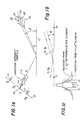
- Figure 1 illustrates creation of a retroreflection surface image and the generation of "primary" and “secondary” image signatures which are further described in the referenced paper by Reynolds and Hageniers.
- the "point" light source 10 which illuminates surface 11 with radiation which is reflected and then retroreflected by retroreflecting member (typically a screen) 12, containing a large number of small retroreflecting elements which are generally small relative to the extension of surface that is being measured (e.g. 50 micron diameter elements and surface areas 50mm or more).
- retroreflecting member typically a screen
- the light from the sloped protuding portion of the surface is directed to other points (e.g. P A , P B ) of the retroreflective screen than would normally have been illuminated by light reflected from that portion of the surface, had the surface not been distorted.
- the light from this and all portions of the screen returns to the general region of the surface from whence it came, however covering an area generally larger than the up-dent, due to a typical divergence ⁇ of ⁇ 1/2 degree of returned light from the screen.
- there may be little or no returned light realizing that if the slope of the up-dent is sufficiently great (relative to the screen extension), light (e.g. proceeding to point P A ) can completely exit the system (i.e. not able to hit the screen at all or at a suitable angle for retroreflection).
- the primary signature of an up-ding for example, however appears to be shifted from the true location of the defect. It appears to lie farther from (or closer to) the observer depending on whether the light source is at a smaller (or larger) angle from the surface than the observer.
- the amount of displacement is proportional to the angular separation in the illumination and observation axes. For "off-axis" operation ( ⁇ ), this makes it difficult to use the primary signature when one wants to determine a defect position on the surface (and say correct it using a grinder or whatever to grind off the area of defect, e.g. on a sheet metal panel).
- the point source creates the sharpest contrast defect and makes the process of finding small defects of sharper slope easiest (at least where few other defects are present).
- a point light source generally should not be used. The same holds true in "off-axis" mode where one wishes to know accurately where on the panel the defect indication is from.
- Illustrated in Figure 4 is a novel method for assisting operators to utilize the invention. It is often desirable to take a test part and position it back where an original master part for example had been, with the master part retroreflection surface image digitally stored on a disk 405 for example, used as a reference.
Landscapes
- Physics & Mathematics (AREA)
- Health & Medical Sciences (AREA)
- Life Sciences & Earth Sciences (AREA)
- Chemical & Material Sciences (AREA)
- Analytical Chemistry (AREA)
- Biochemistry (AREA)
- General Health & Medical Sciences (AREA)
- General Physics & Mathematics (AREA)
- Immunology (AREA)
- Pathology (AREA)
- Investigating Materials By The Use Of Optical Means Adapted For Particular Applications (AREA)
Priority Applications (1)
| Application Number | Priority Date | Filing Date | Title |
|---|---|---|---|
| EP90108857A EP0455857A1 (fr) | 1990-05-11 | 1990-05-11 | Appareil et procédés améliorés d'inspection de surface et de mesure des distortions de manière rétroréflective |
Applications Claiming Priority (1)
| Application Number | Priority Date | Filing Date | Title |
|---|---|---|---|
| EP90108857A EP0455857A1 (fr) | 1990-05-11 | 1990-05-11 | Appareil et procédés améliorés d'inspection de surface et de mesure des distortions de manière rétroréflective |
Publications (1)
| Publication Number | Publication Date |
|---|---|
| EP0455857A1 true EP0455857A1 (fr) | 1991-11-13 |
Family
ID=8203968
Family Applications (1)
| Application Number | Title | Priority Date | Filing Date |
|---|---|---|---|
| EP90108857A Withdrawn EP0455857A1 (fr) | 1990-05-11 | 1990-05-11 | Appareil et procédés améliorés d'inspection de surface et de mesure des distortions de manière rétroréflective |
Country Status (1)
| Country | Link |
|---|---|
| EP (1) | EP0455857A1 (fr) |
Cited By (6)
| Publication number | Priority date | Publication date | Assignee | Title |
|---|---|---|---|---|
| KR20030060243A (ko) * | 2002-01-07 | 2003-07-16 | 엘지전자 주식회사 | 평판 디스플레이 자동 검사장치 |
| DE102004029212A1 (de) * | 2004-06-16 | 2006-01-12 | Leica Microsystems Semiconductor Gmbh | Vorrichtung und Verfahren zur optischen Auf- und/oder Durchlichtinspektion von Mikrostrukturen im IR |
| US7268867B2 (en) | 2004-03-30 | 2007-09-11 | Vistec Semiconductor Systems Gmbh | Apparatus and method for inspecting a semiconductor component |
| US7292328B2 (en) | 2003-12-19 | 2007-11-06 | Vistec Semiconductor Systems Gmbh | Method for inspection of a wafer |
| US7489394B2 (en) | 2005-03-31 | 2009-02-10 | Vistec Semiconductor Systems Gmbh | Apparatus for inspecting a disk-like object |
| DE102008028869A1 (de) | 2008-06-19 | 2009-12-24 | Vistec Semiconductor Systems Gmbh | Verfahren und Vorrichtung zur Inspektion eines scheibenförmigen Gegenstandes |
Citations (2)
| Publication number | Priority date | Publication date | Assignee | Title |
|---|---|---|---|---|
| WO1986005588A1 (fr) * | 1985-03-14 | 1986-09-25 | Diffracto Ltd. | Perfectionnements apportes au procede ''diffractosight'' |
| WO1987000629A1 (fr) * | 1985-07-15 | 1987-01-29 | Sira Limited | Appareil de controle |
-
1990
- 1990-05-11 EP EP90108857A patent/EP0455857A1/fr not_active Withdrawn
Patent Citations (2)
| Publication number | Priority date | Publication date | Assignee | Title |
|---|---|---|---|---|
| WO1986005588A1 (fr) * | 1985-03-14 | 1986-09-25 | Diffracto Ltd. | Perfectionnements apportes au procede ''diffractosight'' |
| WO1987000629A1 (fr) * | 1985-07-15 | 1987-01-29 | Sira Limited | Appareil de controle |
Cited By (8)
| Publication number | Priority date | Publication date | Assignee | Title |
|---|---|---|---|---|
| KR20030060243A (ko) * | 2002-01-07 | 2003-07-16 | 엘지전자 주식회사 | 평판 디스플레이 자동 검사장치 |
| US7292328B2 (en) | 2003-12-19 | 2007-11-06 | Vistec Semiconductor Systems Gmbh | Method for inspection of a wafer |
| US7268867B2 (en) | 2004-03-30 | 2007-09-11 | Vistec Semiconductor Systems Gmbh | Apparatus and method for inspecting a semiconductor component |
| DE102004029212A1 (de) * | 2004-06-16 | 2006-01-12 | Leica Microsystems Semiconductor Gmbh | Vorrichtung und Verfahren zur optischen Auf- und/oder Durchlichtinspektion von Mikrostrukturen im IR |
| DE102004029212B4 (de) * | 2004-06-16 | 2006-07-13 | Leica Microsystems Semiconductor Gmbh | Vorrichtung und Verfahren zur optischen Auf- und/oder Durchlichtinspektion von Mikrostrukturen im IR |
| US8154718B2 (en) | 2004-06-16 | 2012-04-10 | Vistec Semiconductor Systems Gmbh | Apparatus and method for inspecting micro-structured devices on a semiconductor substrate |
| US7489394B2 (en) | 2005-03-31 | 2009-02-10 | Vistec Semiconductor Systems Gmbh | Apparatus for inspecting a disk-like object |
| DE102008028869A1 (de) | 2008-06-19 | 2009-12-24 | Vistec Semiconductor Systems Gmbh | Verfahren und Vorrichtung zur Inspektion eines scheibenförmigen Gegenstandes |
Similar Documents
| Publication | Publication Date | Title |
|---|---|---|
| EP0174939B2 (fr) | Detection de defauts a la surface de panneaux | |
| US3781110A (en) | Optical range finding system | |
| US4732473A (en) | Apparatus for, and methods of, determining the characteristics of semi-conductor wafers | |
| EP1582854B1 (fr) | Système et procédé pour messurer des obstructions optique | |
| US4838679A (en) | Apparatus for, and method of, examining eyes | |
| EP0571431B1 (fr) | Capteur optique | |
| JP4425351B2 (ja) | 反射表面の経路を測定する方法及び装置 | |
| EP1061329A2 (fr) | Procédé et système de mesure automatique et sans contact des propriétés optiques des objets optiques | |
| EP1505425A1 (fr) | Dispositif et méthode pour réduire le Speckle | |
| DE19944354A1 (de) | Verfahren und Vorrichtung zur Ermittlung der Form oder der Abbildungseigenschaften von spiegelnden oder transparenten Objekten | |
| KR20110029057A (ko) | 영상촬영장치 | |
| WO2006038196A1 (fr) | Examen optique de surfaces d'essai | |
| US8081840B2 (en) | Appliance for controlling transparent or reflective elements | |
| US5074661A (en) | Methods and apparatus for retroreflective surface inspection and distortion measurement | |
| US5206700A (en) | Methods and apparatus for retroreflective surface inspection and distortion measurement | |
| CN104359424B (zh) | 一种椭球镜面形检测装置及方法 | |
| JPH10513287A (ja) | 物体のイメージ、画像を記録、撮像のための方法及び装置 | |
| KR100849921B1 (ko) | 목적물의 스펙트럼 방사의 공간 분포를 측정하는 장치 | |
| EP0455857A1 (fr) | Appareil et procédés améliorés d'inspection de surface et de mesure des distortions de manière rétroréflective | |
| JP2001281101A (ja) | 空間分解能により屈折力を決定するための装置および方法 | |
| EP0502162B1 (fr) | Mesures de distance selon la technique moire utilisant un reseau imprime ou fixe a une surface | |
| JP2932307B2 (ja) | 逆反射を利用した表面検査及び歪み測定のための方法及び装置 | |
| EP4246087B1 (fr) | Procédé et dispositif de caractérisation d'une surface d'un objet | |
| EP0901639B1 (fr) | Procede et dispositif pour la determination de la direction dans laquelle se trouve un objet | |
| KR101555542B1 (ko) | 평판패널 검사장치 |
Legal Events
| Date | Code | Title | Description |
|---|---|---|---|
| PUAI | Public reference made under article 153(3) epc to a published international application that has entered the european phase |
Free format text: ORIGINAL CODE: 0009012 |
|
| AK | Designated contracting states |
Kind code of ref document: A1 Designated state(s): BE DE FR GB NL SE |
|
| 17P | Request for examination filed |
Effective date: 19911205 |
|
| 17Q | First examination report despatched |
Effective date: 19940127 |
|
| STAA | Information on the status of an ep patent application or granted ep patent |
Free format text: STATUS: THE APPLICATION IS DEEMED TO BE WITHDRAWN |
|
| 18D | Application deemed to be withdrawn |
Effective date: 19940607 |