EP0456207A2 - Circuit d'entrée d'adaptation et méthode pour l'ajuster - Google Patents
Circuit d'entrée d'adaptation et méthode pour l'ajuster Download PDFInfo
- Publication number
- EP0456207A2 EP0456207A2 EP91107478A EP91107478A EP0456207A2 EP 0456207 A2 EP0456207 A2 EP 0456207A2 EP 91107478 A EP91107478 A EP 91107478A EP 91107478 A EP91107478 A EP 91107478A EP 0456207 A2 EP0456207 A2 EP 0456207A2
- Authority
- EP
- European Patent Office
- Prior art keywords
- amplifier
- open stub
- input matching
- matching network
- electrical length
- Prior art date
- Legal status (The legal status is an assumption and is not a legal conclusion. Google has not performed a legal analysis and makes no representation as to the accuracy of the status listed.)
- Granted
Links
Images




Classifications
-
- H—ELECTRICITY
- H01—ELECTRIC ELEMENTS
- H01P—WAVEGUIDES; RESONATORS, LINES, OR OTHER DEVICES OF THE WAVEGUIDE TYPE
- H01P5/00—Coupling devices of the waveguide type
- H01P5/02—Coupling devices of the waveguide type with invariable factor of coupling
Definitions
- the present invention relates to an input matching network (circuit) in an input circuit of a low noise amplifier used in a down-converter for use in a direct broadcast satellite (DBS) system.
- DBS direct broadcast satellite
- a noise figure (NF) of an amplifier which uses a field effect transistor (FET) varies with a source impedance as viewed from the FET into the signal source and it is minimum at a certain source impedance.
- This source impedance is called an optimum source impedance Z opt .
- an input matching network in an input circuit of the FET is adjusted such that the source impedance as viewed from the FET is equal to the optimum source impedance Z opt .
- the input matching network in the input circuit of the FET is adjusted such that a source reflection coefficient as viewed from the FET is equal to an optimum source reflection coefficient ⁇ opt .
- the optimum source reflection coefficient ⁇ opt varies with a manufacturing variation of the FET.
- design was made such that the reflection coefficient of the signal source as viewed from the FET is equal to a mean value of the manufacturing variations of the optimum source reflection coefficient ⁇ opt .
- the NF of the amplifier includes a variation and a high manufacturing yield cannot be attained.
- the length and the width of the microstrip line which forms the input matching network may be cut by a YAG laser to adjust the characteristic of the amplifier.
- the prior art technique to adjust the characteristic of the amplifier by forming the adjusting circuit on the ceramic substrate is riched in flexibility but provides a very low productivity.
- the Technique to cut the length or the width of the microstrip line on the monolithic IC by the laser it is not possible to increase the length or the width.
- the input matching network of the present invention uses an open stub as a circuit component.
- a source reflection coefficient as viewed from an input end of an amplifier connected to the stub varies such that a phase angle increases along a constant resistance circle on a Smith Chart.
- the electrical length of the open stub is set such that the phase angle of the source reflection coefficient as viewed from the amplifier is smaller than a mean value of manufacturing variations of the phase angle of the optimum source reflection coefficient of the amplifier, a matching point can be adjusted by reducing the electrical length of the open stub such that it is applicable over a substantially entire distribution of the manufacturing variation of the optimum source reflection coefficient of the amplifier.
- a pulse doped structure GaAs MESFET is used in an amplifier circuit of a low noise amplifier.
- a pulse doped GaAs layer having carriers confined therein is used as an activation layer of the MESFET.
- of an optimum source reflection coefficient ⁇ opt at which the NF is minimum and a phase angle ⁇ opt in the ⁇ opt is shown in Fig. 1.
- the manufacturing variation is due to a manufacturing variation of the FET.
- black dots represent distribution and straight line represents an approximate line of the distribution.
- and angle ⁇ opt there is a strong correlation between
- the input matching network of the low noise amplifier of the present embodiment is designed such that a matching point for impedance-converting an external impedance (50 ⁇ ) moves along the narrow band distribution. More specifically, an open stub is provided in the input matching network, and an electrical length of the open stub is selected such that the matching point by the input matching network is positioned at a point in the distribution of the manufacturing variation of ⁇ opt which assures a minimum angle. In the present embodiment, the minimum angle point is shown by an arrow 40 in Fig. 3.
- the input matching network is constructed such that as the electrical length of the open stub is reduced, the matching point moves substantially along a constant resistance circle of Fig. 3.
- the matching point of the external impedance by the input matching network can move over the entire range of the manufacturing variation of ⁇ opt . Accordingly, the conversion of the external impedance can be adjusted to the minimum NF point by cutting the open stub by a laser for tuning.
- the characteristic of the amplifier can be adjusted by merely shortening the electrical length of the open stub, and the process is most practical and significantly improves a manufacturing yield of a wafer.
- a specific design method of such input matching network is now explained in sequence.
- a circuit configuration to move the matching point substantially along the constant resistance circle of Fig. 3 may be attained by a combination of components but it is preferable to attain it with a minimum number of components, as is done in the present embodiment.
- the open stub functions as a parallel capacitance when the electrical length is smaller than ⁇ /4 (l ⁇ ⁇ ⁇ /4). Accordingly, an impedance Z match as views from the load of the basic input matching network 50 to the signal source varies with the electrical length l ⁇ of the open stub S1.
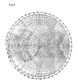
- the impedance Z match moves along an arrow shown on the Smith Chart of Fig. 6 by the change of length.
- the electrical length l ⁇ increase substantially along the direction of the arrow.
- the optimum source reflection coefficient ⁇ opt has a small angle where the amplitude is large, and has a large angle where the amplitude is small. Accordingly, ⁇ opt distribute substantially along the constant resistance circle on the Smith Charts shown in Figs.2 and 3, but distribute inwardly of the circle where the angle is large.
- the input matching network is configured as shown in Fig. 7.
- a serial inductance S2 is connected to the basic input matching network 50.
- the movement on the constant resistance circle may be attained only by the serial inductance, but the series inductance S2 is formed by a strip line having an electrical length of approximately ⁇ /4 in order to convert the parallel capacitance by the open stub S1 to a serial inductance.
- a manner in which the impedance Z open moves by the electrical length l ⁇ of the open stub S1 shown Fig. 7 differs with the impedance Z start .
- the impedances Z open and Z start are impedances as viewed from the chain line position to the signal source. In the Smith Chart shown in Fig. 8, the movement of the impedance Z open changes with the values B, C, D and E of the impedance Z start .
- the electrical length l ⁇ of the open stub S1 increases along the direction of the arrow. As shown in Fig.
- the movement of impedance Z match which are impedances as viewed from a load position to the signal source, also changes with the values F, G, H and I of the impedance Z start .
- the electrical length l ⁇ of the open stub S1 also increases along the direction of the allow.
- serial inductance S3 corresponds to a basic input matching network 50 of Fig. 7 and the impedance Z start moves along the bold arrows shown in Figs.8 and 9 by the adjustment of the length of the serial inductance S3.
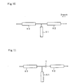
- a capacitor C is inserted between the serial inductances S2 and S3.
- the serial capacitance may be formed by a MIM capacitor (overlay structure). Where a nitride film (Si3N4) having a firm thickness of 3000 ⁇ is used as an interlayer insulation film, the capacitance is approximately 0.2 fF/ ⁇ m2. Thus, when the capacitor C having 0.3 pF is to be formed by this structure, the area is approximately 1500 ⁇ m2.
- the capacitor C may be formed by an interdigital capacitor having comb-shaped electrodes instead of the MIM capacitor.
- the open stub S1 and the serial inductances S2 and S3 may be formed by microstrip lines.
- the series inductance S3 is connected to the signal source, and the serial inductance S2 is connected to the load, that is, the pulse doped structure GaAs MESFET.
- the optimum source reflection coefficient ⁇ opt moves as initially intended as shown in Fig. 3. Accordingly, ⁇ opt moves over the entire range of the manufacturing variation by cutting the electrical length l ⁇ of the open stub set at the minimum angle position by the laser.
- the low noise amplifier having the optimum characteristic is attained by stopping the cutting of the open stub S1 at the minimum NF point. The cutting of the open stub S1 is effected after the wafer manufacturing process.
- Figs.12-15 are Smith Charts for illustrating the movement of ⁇ opt when the electrical length of the open stub S1 is cut at various values of constants of the components of the input matching network shown in Fig. 11.
- the statistical property of the amplitude and the angle of the optimum source power supply reflection coefficient ⁇ opt of the pulse doped structure FET is utilized and the length of the open stub S1 in the input matching network is shortened by the laser cutter so that the NF is optimized to cope with the manufacturing variation of ⁇ opt of the FET. As a result, the low noise amplifier with a high manufacturing yield is attained.
Landscapes
- Microwave Amplifiers (AREA)
Applications Claiming Priority (2)
| Application Number | Priority Date | Filing Date | Title |
|---|---|---|---|
| JP11953390A JPH0414904A (ja) | 1990-05-09 | 1990-05-09 | 低雑音アンプ |
| JP119533/90 | 1990-05-09 |
Publications (3)
| Publication Number | Publication Date |
|---|---|
| EP0456207A2 true EP0456207A2 (fr) | 1991-11-13 |
| EP0456207A3 EP0456207A3 (en) | 1992-11-25 |
| EP0456207B1 EP0456207B1 (fr) | 1995-10-25 |
Family
ID=14763642
Family Applications (1)
| Application Number | Title | Priority Date | Filing Date |
|---|---|---|---|
| EP91107478A Expired - Lifetime EP0456207B1 (fr) | 1990-05-09 | 1991-05-08 | Circuit d'entrée d'adaptation et méthode pour l'ajuster |
Country Status (4)
| Country | Link |
|---|---|
| EP (1) | EP0456207B1 (fr) |
| JP (1) | JPH0414904A (fr) |
| CA (1) | CA2041729A1 (fr) |
| DE (1) | DE69114046T2 (fr) |
Cited By (1)
| Publication number | Priority date | Publication date | Assignee | Title |
|---|---|---|---|---|
| US12525920B2 (en) | 2023-04-28 | 2026-01-13 | Analog Devices, Inc. | Input matching network with harmonic trap for frequency multiplier |
Families Citing this family (1)
| Publication number | Priority date | Publication date | Assignee | Title |
|---|---|---|---|---|
| RU2313867C1 (ru) * | 2006-05-06 | 2007-12-27 | Открытое акционерное общество Центральный научно-исследовательский институт измерительной аппаратуры (ЦНИИИА) | Малогабаритный ступенчатый трансформатор волновых сопротивлений |
-
1990
- 1990-05-09 JP JP11953390A patent/JPH0414904A/ja active Pending
-
1991
- 1991-05-02 CA CA 2041729 patent/CA2041729A1/fr not_active Abandoned
- 1991-05-08 DE DE1991614046 patent/DE69114046T2/de not_active Expired - Fee Related
- 1991-05-08 EP EP91107478A patent/EP0456207B1/fr not_active Expired - Lifetime
Cited By (1)
| Publication number | Priority date | Publication date | Assignee | Title |
|---|---|---|---|---|
| US12525920B2 (en) | 2023-04-28 | 2026-01-13 | Analog Devices, Inc. | Input matching network with harmonic trap for frequency multiplier |
Also Published As
| Publication number | Publication date |
|---|---|
| JPH0414904A (ja) | 1992-01-20 |
| CA2041729A1 (fr) | 1991-11-10 |
| DE69114046D1 (de) | 1995-11-30 |
| EP0456207A3 (en) | 1992-11-25 |
| DE69114046T2 (de) | 1996-04-11 |
| EP0456207B1 (fr) | 1995-10-25 |
Similar Documents
| Publication | Publication Date | Title |
|---|---|---|
| EP0592002B1 (fr) | Circuit intégré à microonde | |
| US4658220A (en) | Dual-gate, field-effect transistor low noise amplifier | |
| US5832376A (en) | Coplanar mixer assembly | |
| US5270667A (en) | Impedance matching and bias feed network | |
| US7173502B2 (en) | Reflection loss suppression circuit | |
| EP1003277B1 (fr) | Multiplicateur de fréquence fournissant des harmoniques supérieures au quatrième ordre de manière efficace et stable | |
| US6946934B2 (en) | Transmission line and semiconductor integrated circuit device | |
| US5289142A (en) | Transmit/receive switch for phased array antenna | |
| US4423388A (en) | RF Amplifier circuit employing FET devices | |
| US5075645A (en) | Matching circuit for high frequency transistor | |
| Hori et al. | GaAs monolithic MIC's for direct broadcast satellite receivers | |
| US5546049A (en) | Frequency scalable pre-matched transistor | |
| CA2067047C (fr) | Circuit oscillant | |
| EP0456207B1 (fr) | Circuit d'entrée d'adaptation et méthode pour l'ajuster | |
| Watkins et al. | A 60 GHz GaAs FET Amplifier | |
| US6522221B1 (en) | Phase shifter, attenuator, and nonlinear signal generator | |
| US4878033A (en) | Low noise microwave amplifier having optimal stability, gain, and noise control | |
| Tserng et al. | Design, fabrication, and characterization of monolithic microwave GaAs power FET amplifiers | |
| Rigby et al. | Broadband monolithic low-noise feedback amplifiers | |
| Komaru et al. | 1 watt compact Ka-band MMIC power amplifiers using lumped element matching circuits | |
| KR100961370B1 (ko) | 고주파용 전송선로 및 이를 이용한 임피던스 변환기 | |
| US7199667B2 (en) | Integrated power amplifier arrangement | |
| JP2654248B2 (ja) | 共平面アンテナ | |
| US4118672A (en) | Attenuation equalizer having constant resistance | |
| Gamand | A complete small size 2 to 30 GHz hybrid distributed amplifier using a novel design technique |
Legal Events
| Date | Code | Title | Description |
|---|---|---|---|
| PUAI | Public reference made under article 153(3) epc to a published international application that has entered the european phase |
Free format text: ORIGINAL CODE: 0009012 |
|
| AK | Designated contracting states |
Kind code of ref document: A2 Designated state(s): DE FR GB NL SE |
|
| PUAL | Search report despatched |
Free format text: ORIGINAL CODE: 0009013 |
|
| AK | Designated contracting states |
Kind code of ref document: A3 Designated state(s): DE FR GB NL SE |
|
| 17P | Request for examination filed |
Effective date: 19930127 |
|
| 17Q | First examination report despatched |
Effective date: 19950113 |
|
| GRAA | (expected) grant |
Free format text: ORIGINAL CODE: 0009210 |
|
| AK | Designated contracting states |
Kind code of ref document: B1 Designated state(s): DE FR GB NL SE |
|
| REF | Corresponds to: |
Ref document number: 69114046 Country of ref document: DE Date of ref document: 19951130 |
|
| ET | Fr: translation filed | ||
| PGFP | Annual fee paid to national office [announced via postgrant information from national office to epo] |
Ref country code: GB Payment date: 19960429 Year of fee payment: 6 |
|
| PGFP | Annual fee paid to national office [announced via postgrant information from national office to epo] |
Ref country code: FR Payment date: 19960510 Year of fee payment: 6 |
|
| PGFP | Annual fee paid to national office [announced via postgrant information from national office to epo] |
Ref country code: DE Payment date: 19960513 Year of fee payment: 6 |
|
| PGFP | Annual fee paid to national office [announced via postgrant information from national office to epo] |
Ref country code: SE Payment date: 19960517 Year of fee payment: 6 |
|
| PGFP | Annual fee paid to national office [announced via postgrant information from national office to epo] |
Ref country code: NL Payment date: 19960529 Year of fee payment: 6 |
|
| PLBE | No opposition filed within time limit |
Free format text: ORIGINAL CODE: 0009261 |
|
| STAA | Information on the status of an ep patent application or granted ep patent |
Free format text: STATUS: NO OPPOSITION FILED WITHIN TIME LIMIT |
|
| 26N | No opposition filed | ||
| PG25 | Lapsed in a contracting state [announced via postgrant information from national office to epo] |
Ref country code: GB Effective date: 19970508 |
|
| PG25 | Lapsed in a contracting state [announced via postgrant information from national office to epo] |
Ref country code: SE Effective date: 19970509 |
|
| PG25 | Lapsed in a contracting state [announced via postgrant information from national office to epo] |
Ref country code: NL Effective date: 19971201 |
|
| GBPC | Gb: european patent ceased through non-payment of renewal fee |
Effective date: 19970508 |
|
| PG25 | Lapsed in a contracting state [announced via postgrant information from national office to epo] |
Ref country code: FR Free format text: LAPSE BECAUSE OF NON-PAYMENT OF DUE FEES Effective date: 19980130 |
|
| EUG | Se: european patent has lapsed |
Ref document number: 91107478.9 |
|
| NLV4 | Nl: lapsed or anulled due to non-payment of the annual fee |
Effective date: 19971201 |
|
| PG25 | Lapsed in a contracting state [announced via postgrant information from national office to epo] |
Ref country code: DE Free format text: LAPSE BECAUSE OF NON-PAYMENT OF DUE FEES Effective date: 19980203 |
|
| REG | Reference to a national code |
Ref country code: FR Ref legal event code: ST |