EP0456857A1 - Circuit numérique avec compensation de potentiel entre deux conducteurs de signaux - Google Patents
Circuit numérique avec compensation de potentiel entre deux conducteurs de signaux Download PDFInfo
- Publication number
- EP0456857A1 EP0456857A1 EP90109255A EP90109255A EP0456857A1 EP 0456857 A1 EP0456857 A1 EP 0456857A1 EP 90109255 A EP90109255 A EP 90109255A EP 90109255 A EP90109255 A EP 90109255A EP 0456857 A1 EP0456857 A1 EP 0456857A1
- Authority
- EP
- European Patent Office
- Prior art keywords
- digital signal
- conductors
- potential
- circuit
- equalization
- Prior art date
- Legal status (The legal status is an assumption and is not a legal conclusion. Google has not performed a legal analysis and makes no representation as to the accuracy of the status listed.)
- Granted
Links
- 239000004020 conductor Substances 0.000 title claims abstract description 58
- 230000000295 complement effect Effects 0.000 claims abstract description 9
- 230000008859 change Effects 0.000 claims description 10
- 238000001208 nuclear magnetic resonance pulse sequence Methods 0.000 claims description 8
- 230000007704 transition Effects 0.000 claims description 7
- 230000000694 effects Effects 0.000 abstract 1
- 230000008901 benefit Effects 0.000 description 3
- 238000011161 development Methods 0.000 description 3
- 230000018109 developmental process Effects 0.000 description 3
- 238000005516 engineering process Methods 0.000 description 3
- 239000008186 active pharmaceutical agent Substances 0.000 description 2
- 108010076504 Protein Sorting Signals Proteins 0.000 description 1
- 230000000903 blocking effect Effects 0.000 description 1
- 230000008878 coupling Effects 0.000 description 1
- 238000010168 coupling process Methods 0.000 description 1
- 238000005859 coupling reaction Methods 0.000 description 1
- 230000003111 delayed effect Effects 0.000 description 1
- 239000011159 matrix material Substances 0.000 description 1
- 238000005457 optimization Methods 0.000 description 1
- 230000009467 reduction Effects 0.000 description 1
Images
Classifications
-
- H—ELECTRICITY
- H04—ELECTRIC COMMUNICATION TECHNIQUE
- H04L—TRANSMISSION OF DIGITAL INFORMATION, e.g. TELEGRAPHIC COMMUNICATION
- H04L25/00—Baseband systems
- H04L25/02—Details ; arrangements for supplying electrical power along data transmission lines
- H04L25/0264—Arrangements for coupling to transmission lines
- H04L25/0272—Arrangements for coupling to multiple lines, e.g. for differential transmission
Definitions
- the invention relates to a digital signal circuit to be implemented in CMOS technology, the circuit arrangement being acted upon by an input digital signal and provided on the output side with two complementary signal conductors which can be loaded by line capacitances and / or load capacitances, a potential equalization being achievable between these conductors via a controllable switching element in an equalization path is.
- the invention now shows a way in which, in the case of a digital signal circuit of the type mentioned at the outset, equipotential bonding can also be achieved without great effort between two lines located at different operating potential sources.
- a digital signal circuit which is supplied with an input digital signal and is provided on the output side with two complementary signal conductors which can be loaded by line capacitances and / or load capacitances, a potential equalization being achievable between these conductors via a controllable switching element in an equalization path, according to the invention achieved in that the potential equalization depends on on the direction of the potential transitions of the output digital signals on the conductors, either via a first or a second compensation path of two mutually antiparallel, controllable and in each case self-locking compensation paths when the potential equalization is reached.
- the invention brings in connection with the advantage that when changing the respective digital signal state a potential equalization between the two conductors via the respective equalization path and further reloading of the two conductors to the respective new operating potential is made possible, the further advantage of reducing the otherwise power dissipation required for conductor reloading, and at the same time a blocking of the relevant compensation path occurs in the event of equipotential bonding, without the need for a special control device.
- the potential swing required to achieve the potential corresponding to the respective output digital signal state is reduced by half.
- the power loss requirement of the digital signal circuit is reduced by 50% compared to the power loss requirement of a digital signal circuit without such a potential equalization option. Due to the short-circuit-like equipotential bonding via the respective equalization path, a higher edge steepness of the output digital signal is also achieved.
- the two equalization paths each consist of a series circuit which is formed with a switching transistor and a self-locking diode, the two switching transistors in the two equalization paths as CMOS transistors of opposite channel type can be formed.
- the compensation paths are controlled in accordance with the input digital signal which is used at the same time for driving conductor-specific driver circuits; this has the advantage of a simple synchronization between the respective control of the conductor-specific driver circuits and the control of the switching transistors in the compensation paths without special power requirements and without special space requirements when integrating the components of the digital signal circuit.
- the conductor-specific driver circuits can each be subdivided into a main driver and an auxiliary driver, the main drivers being controlled by control pulse sequences formed in a gate circuit in such a way that the main drivers each come into the same operating state immediately after a change of state of the auxiliary drivers after reaching the new operating potential on the respective conductor, they reach the tristate state, while the auxiliary drivers are controlled directly in accordance with the input digital signal, which is advantageous in that the division of the conductor-specific driver circuits into main drivers and auxiliary drivers enables to keep the dimensioning of the auxiliary drivers many times smaller than that of the main drivers, thereby reducing the power loss.
- the main drivers each contribute in accordance with the control pulse sequences of the gate circuit to a further reduction in the recharging time of the conductor potentials of the conductors loaded by line capacitances and / or load capacitances in such a way that for the duration of the control pulses via the transistors of the main drivers on the conductors in each case an output digital signal state corresponding complementary operating potential is created.
- the control pulse train forming gate circuit is advantageous without major circuitry out of digital Switching elements such as inverters and logic elements are composed, different signal delay times of the input digital signal and of the output digital signal being achieved by series connection of inverters and linked to control pulse sequences via switching elements.
- Linking the output digital signal to the input digital signal by the gate circuit forming the control pulse sequences and the switching behavior of the logic elements of the gate circuit result in a delayed switch-on of the main drivers and thereby a cross-current-free connection of the respective operating potential sources via the main drivers to the conductors loaded with line capacities and / or load capacities.
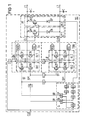
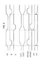
- FIG. 1 schematically shows, in the scope necessary for understanding the invention, a digital signal circuit DS provided on the input side with an input digital signal CL0 ⁇ (FIG. 2, line 1) and on the output side with two conductors L1, L2 which can be loaded by line capacitances and / or load capacitances C; Potential equalization can be achieved via a controllable switching element (S) in an equalization path (PF) between these conductors L1, L2.
- the two conductors L1, L2 are provided with individual driver circuits TR, TRN, which in turn may each be divided into a main driver and an auxiliary driver, as will be explained in more detail below;
- a gate circuit G is provided to form control pulse sequences for the conductor-specific driver circuits.
- two conductors L1, L2 which lead to complementary signal potentials are two antiparallel to one another, controllable and each self-locking compensation paths provided when equipotential bonding is reached.
- the equalization paths can be designed in such a way that in a first equalization path PF1 to a switching element S, which can be an N-channel CMOS switching transistor SN, a normally-off component, e.g. a diode DN, connected in series;
- a switching element S In a second equalization path PF2, the switching element S may be a P-channel CMOS switching transistor SP and the normally-off, series-connected component may be a diode DP.
- the cathode of the diode DN in the first equalization path PF1 and the anode of the diode DP in the second equalization path PF2 are connected directly to the conductor L2 in the embodiment shown in the drawing.
- the gate connections of the CMOS switching transistors SN, SP are acted upon by the negated input digital signal CL0 ⁇ N and cause the switching transistors to be switched through with the result of equipotential bonding between the complementary potential states on the conductors L1, L2 which change in time with the input digital signal.
- the driver circuits TR, TRN which are each divided into a main driver HA1, HA2 and an auxiliary driver HL1, HL2, are acted upon with different signal sequences gp, gnn, gn, gpn, CL0 ⁇ , CL0 ⁇ N (see FIG. 1).
- the main drivers HA1, HA2, each formed with a P-channel transistor HA1P, HA2P and an N-channel transistor HA1N, HA2N, are connected with the control pulse sequences gn, gp formed in a gate circuit G, as shown in FIG.
- the operating potential sources are in each case connected to the source connections of the CMOS switching transistors of the main and auxiliary drivers, the operating potential source VDD being connected to the source connections of the P-channel CMOS transistors HA1P, HL1P, HA2P, HL2P and to the source connections of the N-channel CMOS transistors HA1N, HL1N, HA2N, HL2N the operating potential source DG is present.
- An output digital signal CLN (FIG. 2, line 5) on the line L2, which is complementary to the output digital signal CL (FIG. 2, line 4) on the conductor L1, is in each case effected by complementary control signals of the driver circuits TR, TRN. As can be seen from the signal waveforms in FIG.
- the negated input digital signal CL0 ⁇ N makes the N-channel CMOS switching transistor SN conductive, with the result that the first equalization path PF1 becomes conductive and thus equipotential bonding between the conductor L1 and the conductor L2.
- the diode DN located in the equalization path PF1 causes it to self-lock; then the potential transition continues on each conductor L1, L2 until the new operating potential is reached.
- the diode DP in the equalization path PF2 causes it to self-lock; then the potential transition continues on each conductor L1, L2 until the new operating potential is reached.
Landscapes
- Engineering & Computer Science (AREA)
- Power Engineering (AREA)
- Computer Networks & Wireless Communication (AREA)
- Signal Processing (AREA)
- Electronic Switches (AREA)
- Logic Circuits (AREA)
- Arrangements For Transmission Of Measured Signals (AREA)
Priority Applications (3)
| Application Number | Priority Date | Filing Date | Title |
|---|---|---|---|
| EP90109255A EP0456857B1 (fr) | 1990-05-16 | 1990-05-16 | Circuit numérique avec compensation de potentiel entre deux conducteurs de signaux |
| AT90109255T ATE114098T1 (de) | 1990-05-16 | 1990-05-16 | Digitalschaltung mit potentialausgleich zwischen zwei signalleitern. |
| DE59007700T DE59007700D1 (de) | 1990-05-16 | 1990-05-16 | Digitalschaltung mit Potentialausgleich zwischen zwei Signalleitern. |
Applications Claiming Priority (1)
| Application Number | Priority Date | Filing Date | Title |
|---|---|---|---|
| EP90109255A EP0456857B1 (fr) | 1990-05-16 | 1990-05-16 | Circuit numérique avec compensation de potentiel entre deux conducteurs de signaux |
Publications (2)
| Publication Number | Publication Date |
|---|---|
| EP0456857A1 true EP0456857A1 (fr) | 1991-11-21 |
| EP0456857B1 EP0456857B1 (fr) | 1994-11-09 |
Family
ID=8203987
Family Applications (1)
| Application Number | Title | Priority Date | Filing Date |
|---|---|---|---|
| EP90109255A Expired - Lifetime EP0456857B1 (fr) | 1990-05-16 | 1990-05-16 | Circuit numérique avec compensation de potentiel entre deux conducteurs de signaux |
Country Status (3)
| Country | Link |
|---|---|
| EP (1) | EP0456857B1 (fr) |
| AT (1) | ATE114098T1 (fr) |
| DE (1) | DE59007700D1 (fr) |
Cited By (3)
| Publication number | Priority date | Publication date | Assignee | Title |
|---|---|---|---|---|
| EP0547814A3 (en) * | 1991-12-18 | 1995-04-12 | American Telephone & Telegraph | Balanced line driver for local area networks or the like |
| WO2003096753A1 (fr) * | 2002-05-08 | 2003-11-20 | Siemens Aktiengesellschaft | Ensemble circuit destine au fonctionnement d'un voyant lumineux |
| CN112753199A (zh) * | 2018-09-10 | 2021-05-04 | 伊诺瓦半导体有限责任公司 | 用于数据流控制的高效线路驱动器装置 |
Citations (3)
| Publication number | Priority date | Publication date | Assignee | Title |
|---|---|---|---|---|
| US4525836A (en) * | 1982-12-27 | 1985-06-25 | The Grass Valley Group, Inc. | Circuit for converting a logical signal into two balanced logical signals |
| US4783636A (en) * | 1987-10-02 | 1988-11-08 | Motorola, Inc. | Amplifiers providing balanced output signals |
| EP0345623A2 (fr) * | 1988-06-08 | 1989-12-13 | Siemens Aktiengesellschaft | Dispositif de commutation pour signaux à large bande |
-
1990
- 1990-05-16 AT AT90109255T patent/ATE114098T1/de not_active IP Right Cessation
- 1990-05-16 EP EP90109255A patent/EP0456857B1/fr not_active Expired - Lifetime
- 1990-05-16 DE DE59007700T patent/DE59007700D1/de not_active Expired - Fee Related
Patent Citations (3)
| Publication number | Priority date | Publication date | Assignee | Title |
|---|---|---|---|---|
| US4525836A (en) * | 1982-12-27 | 1985-06-25 | The Grass Valley Group, Inc. | Circuit for converting a logical signal into two balanced logical signals |
| US4783636A (en) * | 1987-10-02 | 1988-11-08 | Motorola, Inc. | Amplifiers providing balanced output signals |
| EP0345623A2 (fr) * | 1988-06-08 | 1989-12-13 | Siemens Aktiengesellschaft | Dispositif de commutation pour signaux à large bande |
Non-Patent Citations (1)
| Title |
|---|
| IEEE INTERNATIONAL CONFERENCE ON COMPUTER DESIGN: VLSI IN COMPUTERS & PROCESSORS, 3. - 5. Oktober 1988, New York, Seiten 344-347, IEEE, New York, US; T.J. GABARA et al.: "High speed, low power CMOS transmitter-receiver system" * |
Cited By (3)
| Publication number | Priority date | Publication date | Assignee | Title |
|---|---|---|---|---|
| EP0547814A3 (en) * | 1991-12-18 | 1995-04-12 | American Telephone & Telegraph | Balanced line driver for local area networks or the like |
| WO2003096753A1 (fr) * | 2002-05-08 | 2003-11-20 | Siemens Aktiengesellschaft | Ensemble circuit destine au fonctionnement d'un voyant lumineux |
| CN112753199A (zh) * | 2018-09-10 | 2021-05-04 | 伊诺瓦半导体有限责任公司 | 用于数据流控制的高效线路驱动器装置 |
Also Published As
| Publication number | Publication date |
|---|---|
| EP0456857B1 (fr) | 1994-11-09 |
| ATE114098T1 (de) | 1994-11-15 |
| DE59007700D1 (de) | 1994-12-15 |
Similar Documents
| Publication | Publication Date | Title |
|---|---|---|
| DE69418020T2 (de) | Ausgangspufferkreis, Eingangspufferkreis und Zweirichtungspufferkreis für mehrere Spannungssysteme | |
| DE69412667T2 (de) | Überspannungstolerante Ausgangspufferschaltung | |
| DE2544974C3 (de) | Schaltkreis zur Realisierung logischer Funktionen | |
| EP0504470B1 (fr) | Circuit translateurs de niveau | |
| DE3342336A1 (de) | Schnittstellenschaltung | |
| DE3743969A1 (de) | Ausgabepuffer | |
| DE2657948C3 (de) | Logikschaltung | |
| DE3228013A1 (de) | Treiberschaltung fuer eine sammelleitung | |
| DE2647982A1 (de) | Logische schaltungsanordnung in integrierter mos-schaltkreistechnik | |
| EP0122946A1 (fr) | Additionneur binaire en CMOS | |
| EP0424554A1 (fr) | Convertisseur série-parallèle et/ou parallèle-série à plusieurs étages | |
| DE19700045A1 (de) | CMOS-Ausgangspuffer mit hoher Stromsteuerfähgikeit bei niedrigem Rauschen | |
| EP0589221B1 (fr) | Dispositif à circuit intégré semi-conducteur | |
| DE68920208T2 (de) | Konfiguration für TTL-Ausgangstreibergatter. | |
| DE4010145C1 (fr) | ||
| EP0456857B1 (fr) | Circuit numérique avec compensation de potentiel entre deux conducteurs de signaux | |
| DE69426720T2 (de) | Halbleiterschaltungsanordnung mit einer Kombination von CMOS- und bipolaren Schaltungen | |
| DE3741913C2 (de) | CMOS-Logikschaltung | |
| EP0345623A2 (fr) | Dispositif de commutation pour signaux à large bande | |
| EP0176909B1 (fr) | Porte ET pour circuits ECL | |
| DE19743347C2 (de) | RS-Flip-Flop mit Enable-Eingängen | |
| EP0689291B1 (fr) | Circuit d'attaque du type MOS | |
| EP0249837A1 (fr) | Dispositif de commutation pour signaux à large bande | |
| EP0766399B1 (fr) | Circuit d'attaque bidirectionnel pour système de bus PCI | |
| DE2448099A1 (de) | Dekodierschaltung mit komplementaeren feldeffekttransistoren |
Legal Events
| Date | Code | Title | Description |
|---|---|---|---|
| PUAI | Public reference made under article 153(3) epc to a published international application that has entered the european phase |
Free format text: ORIGINAL CODE: 0009012 |
|
| 17P | Request for examination filed |
Effective date: 19901205 |
|
| AK | Designated contracting states |
Kind code of ref document: A1 Designated state(s): AT BE CH DE FR GB IT LI NL SE |
|
| 17Q | First examination report despatched |
Effective date: 19940217 |
|
| GRAA | (expected) grant |
Free format text: ORIGINAL CODE: 0009210 |
|
| AK | Designated contracting states |
Kind code of ref document: B1 Designated state(s): AT BE CH DE FR GB IT LI NL SE |
|
| REF | Corresponds to: |
Ref document number: 114098 Country of ref document: AT Date of ref document: 19941115 Kind code of ref document: T |
|
| REF | Corresponds to: |
Ref document number: 59007700 Country of ref document: DE Date of ref document: 19941215 |
|
| ITF | It: translation for a ep patent filed | ||
| ET | Fr: translation filed | ||
| GBT | Gb: translation of ep patent filed (gb section 77(6)(a)/1977) |
Effective date: 19950113 |
|
| PLBE | No opposition filed within time limit |
Free format text: ORIGINAL CODE: 0009261 |
|
| STAA | Information on the status of an ep patent application or granted ep patent |
Free format text: STATUS: NO OPPOSITION FILED WITHIN TIME LIMIT |
|
| 26N | No opposition filed | ||
| PGFP | Annual fee paid to national office [announced via postgrant information from national office to epo] |
Ref country code: GB Payment date: 19970418 Year of fee payment: 8 |
|
| PGFP | Annual fee paid to national office [announced via postgrant information from national office to epo] |
Ref country code: AT Payment date: 19970512 Year of fee payment: 8 |
|
| PGFP | Annual fee paid to national office [announced via postgrant information from national office to epo] |
Ref country code: SE Payment date: 19970516 Year of fee payment: 8 |
|
| PGFP | Annual fee paid to national office [announced via postgrant information from national office to epo] |
Ref country code: FR Payment date: 19970521 Year of fee payment: 8 |
|
| PGFP | Annual fee paid to national office [announced via postgrant information from national office to epo] |
Ref country code: NL Payment date: 19970523 Year of fee payment: 8 |
|
| PGFP | Annual fee paid to national office [announced via postgrant information from national office to epo] |
Ref country code: BE Payment date: 19970527 Year of fee payment: 8 |
|
| PGFP | Annual fee paid to national office [announced via postgrant information from national office to epo] |
Ref country code: DE Payment date: 19970721 Year of fee payment: 8 |
|
| PGFP | Annual fee paid to national office [announced via postgrant information from national office to epo] |
Ref country code: CH Payment date: 19970819 Year of fee payment: 8 |
|
| PG25 | Lapsed in a contracting state [announced via postgrant information from national office to epo] |
Ref country code: GB Free format text: LAPSE BECAUSE OF NON-PAYMENT OF DUE FEES Effective date: 19980516 Ref country code: AT Free format text: LAPSE BECAUSE OF NON-PAYMENT OF DUE FEES Effective date: 19980516 |
|
| PG25 | Lapsed in a contracting state [announced via postgrant information from national office to epo] |
Ref country code: SE Free format text: LAPSE BECAUSE OF NON-PAYMENT OF DUE FEES Effective date: 19980517 |
|
| PG25 | Lapsed in a contracting state [announced via postgrant information from national office to epo] |
Ref country code: LI Free format text: LAPSE BECAUSE OF NON-PAYMENT OF DUE FEES Effective date: 19980531 Ref country code: FR Free format text: LAPSE BECAUSE OF NON-PAYMENT OF DUE FEES Effective date: 19980531 Ref country code: CH Free format text: LAPSE BECAUSE OF NON-PAYMENT OF DUE FEES Effective date: 19980531 Ref country code: BE Free format text: LAPSE BECAUSE OF NON-PAYMENT OF DUE FEES Effective date: 19980531 |
|
| BERE | Be: lapsed |
Owner name: SIEMENS A.G. Effective date: 19980531 |
|
| PG25 | Lapsed in a contracting state [announced via postgrant information from national office to epo] |
Ref country code: NL Free format text: LAPSE BECAUSE OF NON-PAYMENT OF DUE FEES Effective date: 19981201 |
|
| GBPC | Gb: european patent ceased through non-payment of renewal fee |
Effective date: 19980516 |
|
| REG | Reference to a national code |
Ref country code: CH Ref legal event code: PL |
|
| EUG | Se: european patent has lapsed |
Ref document number: 90109255.1 |
|
| NLV4 | Nl: lapsed or anulled due to non-payment of the annual fee |
Effective date: 19981201 |
|
| PG25 | Lapsed in a contracting state [announced via postgrant information from national office to epo] |
Ref country code: DE Free format text: LAPSE BECAUSE OF NON-PAYMENT OF DUE FEES Effective date: 19990302 |
|
| REG | Reference to a national code |
Ref country code: FR Ref legal event code: ST |
|
| PG25 | Lapsed in a contracting state [announced via postgrant information from national office to epo] |
Ref country code: IT Free format text: LAPSE BECAUSE OF NON-PAYMENT OF DUE FEES;WARNING: LAPSES OF ITALIAN PATENTS WITH EFFECTIVE DATE BEFORE 2007 MAY HAVE OCCURRED AT ANY TIME BEFORE 2007. THE CORRECT EFFECTIVE DATE MAY BE DIFFERENT FROM THE ONE RECORDED. Effective date: 20050516 |