EP0456923B1 - Système d'affichage - Google Patents
Système d'affichage Download PDFInfo
- Publication number
- EP0456923B1 EP0456923B1 EP19900305158 EP90305158A EP0456923B1 EP 0456923 B1 EP0456923 B1 EP 0456923B1 EP 19900305158 EP19900305158 EP 19900305158 EP 90305158 A EP90305158 A EP 90305158A EP 0456923 B1 EP0456923 B1 EP 0456923B1
- Authority
- EP
- European Patent Office
- Prior art keywords
- display
- display device
- logic
- control
- adapter
- Prior art date
- Legal status (The legal status is an assumption and is not a legal conclusion. Google has not performed a legal analysis and makes no representation as to the accuracy of the status listed.)
- Revoked
Links
- 230000004044 response Effects 0.000 claims description 22
- 238000004891 communication Methods 0.000 claims description 13
- 230000000007 visual effect Effects 0.000 claims description 7
- 238000010586 diagram Methods 0.000 description 2
- 238000012546 transfer Methods 0.000 description 2
- 230000009118 appropriate response Effects 0.000 description 1
- 238000004590 computer program Methods 0.000 description 1
- 238000013500 data storage Methods 0.000 description 1
- 238000002405 diagnostic procedure Methods 0.000 description 1
- 239000004973 liquid crystal related substance Substances 0.000 description 1
- 238000004519 manufacturing process Methods 0.000 description 1
- 238000000034 method Methods 0.000 description 1
- 230000002093 peripheral effect Effects 0.000 description 1
- 238000012545 processing Methods 0.000 description 1
- 230000001360 synchronised effect Effects 0.000 description 1
- 238000012360 testing method Methods 0.000 description 1
Images

Classifications
-
- G—PHYSICS
- G09—EDUCATION; CRYPTOGRAPHY; DISPLAY; ADVERTISING; SEALS
- G09G—ARRANGEMENTS OR CIRCUITS FOR CONTROL OF INDICATING DEVICES USING STATIC MEANS TO PRESENT VARIABLE INFORMATION
- G09G5/00—Control arrangements or circuits for visual indicators common to cathode-ray tube indicators and other visual indicators
- G09G5/003—Details of a display terminal, the details relating to the control arrangement of the display terminal and to the interfaces thereto
- G09G5/006—Details of the interface to the display terminal
-
- G—PHYSICS
- G09—EDUCATION; CRYPTOGRAPHY; DISPLAY; ADVERTISING; SEALS
- G09G—ARRANGEMENTS OR CIRCUITS FOR CONTROL OF INDICATING DEVICES USING STATIC MEANS TO PRESENT VARIABLE INFORMATION
- G09G2370/00—Aspects of data communication
- G09G2370/04—Exchange of auxiliary data, i.e. other than image data, between monitor and graphics controller
-
- G—PHYSICS
- G09—EDUCATION; CRYPTOGRAPHY; DISPLAY; ADVERTISING; SEALS
- G09G—ARRANGEMENTS OR CIRCUITS FOR CONTROL OF INDICATING DEVICES USING STATIC MEANS TO PRESENT VARIABLE INFORMATION
- G09G2370/00—Aspects of data communication
- G09G2370/04—Exchange of auxiliary data, i.e. other than image data, between monitor and graphics controller
- G09G2370/042—Exchange of auxiliary data, i.e. other than image data, between monitor and graphics controller for monitor identification
Definitions
- the present invention is related to a display system in which control data is communicated between a computer system and a display device.
- the control data includes parameters for specifying the geometry and resolution of an image presented on the display device.
- a display system comprising a raster-scanned display device such as a Cathode Ray Tube (CRT) display device
- these parameters are determined by the rates and amplitudes of horizontal and vertical scan signals generated for producing the raster scan by electrical circuits in the display device.
- the scan signals are synchronised to video signals from a video source such as a computer system by synchronisation (sync) pulses also generated by the video source.
- Some display devices can only operate in a single display mode in accordance with a single set of parameters. Other display devices can be configured to operate in any one of a number of display modes characterised by different sets of parameters. The latter will hereinafter be referred to as multiple mode display devices.
- a display device controlled by a computer system it is desirable for the computer system to identify the type of the display device so that appropriate video and sync signals can be generated.
- Many examples of such computer systems including the IBM PS 2 range, comprise a video graphics adapter (VGA adapter) having an output port for connecting video and sync signals to a display device.
- the VGA adapter also has logic responsive to the manner in which identification pins in the output port are terminated when connected to the display device. The logic identifies the type of display device connected to the VGA adapter from these terminations.
- UK Patent No.2,162,026 describes an example of a display system employing a multiple-mode display device receiving video and sync signals from a computer system display adapter.
- the display device can operate in any one of four display modes.
- the computer system can be instructed to provide sync pulses of either positive or negative polarities. Each polarity combination indicates a different display mode.
- the display device includes decoding logic for configuring the display device to operate in a particular display mode in response to predetermined sync pulse polarities.
- the display systems of the prior art have the disadvantage that the display interfaces of the prior art can identify, and therefore generate appropriate control signals for, only a limited number different display devices. This limitation arises because the number of pins available for display device identification and control is limited by the physical form of the output port.
- An object of the present invention is therefore to provide a display system having a display adapter which is potentially compatible with an unlimited variety of display devices.
- a display system comprising a display device for generating a visual output in response to a plurality of data signals defining the data to be displayed, a display adapter circuit for generating the data signals in a form specified by control data, the control data being unique to the display device, an output port for transmitting the data signals from the display adapter circuit to the display device and for transmitting the control data from the display device to the display adapter circuit, characterised in that the display system further comprises a non-volatile memory located in the display device for storing the extended control data in the form of a plurality of control codes, and communication logic for communicating the control codes between the memory and the output port in response to command signals generated by the display adapter circuit.
- the communication logic comprises a serial data link for communicating the control code between the display device and the output port, device control logic for communicating the control code between the memory and the serial data link, and adapter control logic for communicating the control code between the serial data link and the display adapter circuit.
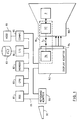
- the computer system includes a central processing unit (CPU) 80 for executing programmed instructions.
- a bus architecture 86 provides a data communication path between the CPU 80 and other components of the display system.
- a read only memory (ROS) 81 provides secure storage of data.
- a random access memory 82 provides temporary data storage.
- Data communication with a host computer system 93 is provided by a communication adapter 85.
- An I/O adapter 84 enables data to pass between the bus architecture 86 and a peripheral device such as a disk file 83.
- a user can operate the computer system using a keyboard 91 which is connected to the bus architecture 86 by a keyboard adapter 90.
- the CRT display device 88 provides a visual output from the display system.
- a display adapter 92 generates video and sync signals at an output port 94 for enabling the display device 88 to generate the visual output.
- the display device 88 comprises a Non-Volatile Memory (NVM) 9 for storing display information in the form of digital codes.
- NVM Non-Volatile Memory
- the display information is communicated between the display device 88 and the display adapter 92 along a serial link 3 which is controlled by communication logic 95.
- the serial link 3 is separate from the lines carrying the video and sync signals from the display adapter 92 to the display device.
- the communication logic 95 is divided into adapter logic 96 and device logic 97. In operation, the adapter logic 96 initiates commands for both reading and writing data to the NVM 9 and the device logic 97 responds accordingly.
- the adapter logic 96 comprises a device driver 1 for generating a command code 21 in response to a program instruction.
- a first serialiser 2 translates the command code 21 into a command bit stream 22 for a first line driver 4 to communicate to the device logic 97 along the serial link 3.
- the device logic 97 comprises a second receiver 5 for detecting the command bit stream 22.
- a second deserialiser 6 translates the command bit stream 22 back into the command code 21.
- a command decoder 7 decodes the command code 21 into an NVM address 8. Address space in the NVM 9 is divided into a personality NVM 10 and a program NVM 11.
- the personality NVM 10 contains identification codes for providing the display system with a specification of the display device 88 connected to the display adapter 92. Each identification code is stored in a different address location.
- the identification codes include coded timing parameters for enabling the display adapter 92 to generate appropriate video and sync signals. Specifically, the timing parameters include sync pulse widths, active video periods, and blanking intervals.
- the identification codes also include a coded transfer parameter for indicating the maximum rate at which the device logic 97 can read or write data to the serial link 3. By reading the transfer parameter before issuing any further commands, the adapter logic 96 can ensure that data is subsequently transferred between the display device 88 and the display adapter 92 at a rate which is compatible with both the adapter logic 96 and the device logic 97.
- Each timing parameter is stored in the form of a sixteen bit identification code. Fifteen bits of the code specify the value of the timing parameter and the sixteenth bit specifies the polarity. It will be appreciated that less critical timing parameters may be stored in the form of eight bit codes or less.
- the personality NVM stores several sets of timing parameters corresponding to different display modes of the display device.
- the program NVM 11 stores control codes for instructing a display input/output (I/O) circuit 12 to adjust drive signals generated by drive circuitry 13 in the display device. Examples of such drive signals directly affect the height, width, and brightness of the visual ouput from the display device 88. Each control code is stored in a different address location. By instructing the display I/O circuit 12 with appropriate control codes, the visual output of the display device 88 can be switched between different display modes under the control of a computer program.
- the program NVM 11 also stores control codes for instructing the display I/O circuit 12 to generate sample codes representative of drive signal magnitudes at predetermined nodes of the drive circuitry 13. It will be appreciated that such control codes may be used to automate diagnostic methods for testing the operation of the display device 88 after manufacture or repair.
- the device logic 97 When the adapter logic 96 issues a read command, the device logic 97 responds by placing an appropriate response code 23 on the serial link 3.
- the response code 23 may either be an identification code 20 from the personality NVM or a sampled data code 19 from the display I/O circuit 12 depending on the nature of the read command.
- the device logic 97 comprises parity logic 14 for adding a parity bit to the response code 23.
- a second serialiser 15 translates the response code 23 into a response bit stream 24.
- the response bit stream 24 is placed on the serial link 3 by a second line driver 16.
- a first receiver 17 detects the response bit stream 24 on the serial link 3.
- a first deserialiser 18 translates the detected response bit stream 24 back into the response code 23 which is decoded by the device driver 1.
- the first serialiser and the first deserialiser of the adapter logic can be combined in a single integrated circuit module, and a similar module can be used to implement the second serialiser and the second deserialiser.
- the first line driver and the first receiver can also be incorporated in a single integrated module, and a similar driver/receiver module can be used to implement the second line driver and the second receiver.
- the adapter logic 96 can be configured to receive a response from the device logic 97 in either a "Handshaking" mode or a "Data-streaming” mode.
- the device logic 97 waits for the adaptor logic to place an acknowledgement code on the serial link 3 before sending the next byte of the response.
- the device logic 97 waits for the adapter logic 96 to acknowledge receiving a block of bytes of the response before sending the next block.
- display information is communicated between the display adapter 92 and the display device 88 by communication logic 95 comprising a serial link 3 which is separate from the lines carrying the video and sync signal from the display adapter 92 to the display device. It will be appreciated however that other communication links and coding methods may be used. Furthermore, the example of the present invention includes a raster-scanned display device. It will be appreciated that the present invention is equally applicable to other display devices such as Liquid Crystal Display device or vector-scanned display devices.
Landscapes
- Engineering & Computer Science (AREA)
- Physics & Mathematics (AREA)
- Computer Hardware Design (AREA)
- General Physics & Mathematics (AREA)
- Theoretical Computer Science (AREA)
- Controls And Circuits For Display Device (AREA)
- Control Of Indicators Other Than Cathode Ray Tubes (AREA)
- Digital Computer Display Output (AREA)
Claims (11)
- Système d'affichage comprenant
un dispositif d'affichage (88) pour générer une sortie visuelle en réponse à une pluralité de signaux de données définissant les données à afficher,
un circuit adaptateur d'affichage (92) pour générer les signaux de données sous une forme spécifiée par des données de contrôle identifiant le dispositif d'affichage (88),
un port de sortie (94) pour transmettre les signaux de données du circuit adaptateur d'affichage (92) au dispositif d'affichage (88) et pour transmettre les données de contrôle du dispositif d'affichage (88) au circuit adaptateur d'affichage (92),
caractérisé en ce que le système d'affichage comporte en outre
une mémoire non volatile (9) disposée dans le dispositif d'affichage (88) pour mémoriser les données de contrôle sous la forme d'une pluralité de codes de contrôle, et
une logique de communication (95) pour communiquer un code de contrôle entre la mémoire et le port de sortie (94) en réponse à un signal de commande (21) généré par le circuit adaptateur d'affichage (92). - Système d'affichage tel que revendiqué dans la revendication 1, dans lequel la logique de communication comprend un lien de données série (3) pour communiquer le code de contrôle entre le dispositif d'affichage et le port de sortie,
une logique de dispositif (97) disposée dans le dispositif d'affichage pour communiquer le code de contrôle entre la mémoire et le lien de données série et
une logique d'adaptateur (96) disposée dans le circuit adaptateur d'affichage pour communiquer le code de contrôle entre le lien de données série et le circuit adaptateur d'affichage. - Système d'affichage tel que revendiqué dans la revendication 2, dans lequel la logique d'adaptateur comprend un premier sérialiseur pour traduire un signal de commande (21) en un flux de bits de commande (22), un premier circuit de pilotage de ligne connecté au port de sortie pour communiquer le flux de bits de commande (22) à la logique de dispositif sur le lien série, un premier récepteur connecté au port de sortie pour recevoir un flux de bits de contrôle de la logique de dispositif sur le lien série, et un premier désérialiseur pour traduire le flux de bits de contrôle en un code de contrôle correspondant au signal de commande (21),
et dans lequel le dispositif logique comprend un second récepteur pour recevoir le flux de bits de commande (22) du port de sortie sur le lien série, un second désérialiseur pour traduire le flux de bits de commande (22) en un signal de commande (21), un décodeur de commande pour traduire le signal de commande (21) en une adresse mémoire pour accéder au code de contrôle mémorisé, un second sérialiseur pour traduire le code de contrôle en flux de bits de contrôle, un second circuit de pilotage de ligne connecté pour communiquer le flux de bits de contrôle au port de sortie sur le lien série. - Système d'affichage tel que revendiqué dans la revendication 3, dans lequel le premier sérialiseur et le premier désérialiseur sont combinés en un module de circuit intégré unique, et dans lequel le second sérialiseur et le second désérialiseur sont combinés en un module de circuit intégré unique.
- Système d'affichage tel que revendiqué dans la revendication 4 ou la revendication 5, dans lequel le premier circuit de pilotage de ligne et le premier récepteur sont incorporés dans un module de circuit intégré unique, et dans lequel le second circuit de pilotage de ligne et le second récepteur sont incorporés dans un module de circuit intégré unique.
- Système d'affichage tel que revendiqué dans la revendication 2, comprenant en outre des moyens pour configurer le dispositif d'affichage pour fonctionner dans des modes d'affichage différents en réponse à des signaux de contrôle de mode communiqués par la logique d'adaptateur à la logique de dispositif sur le lien série.
- Dispositif d'affichage tel que revendiqué dans la revendication 2 ou la revendication 6, comprenant en outre des moyens pour ajuster les paramètres de fonctionnement du circuit de pilotage du dispositif d'affichage en réponse à des signaux de contrôle de paramètre communiqués par la logique d'adaptateur à la logique de dispositif sur le lien série.
- Dispositif d'affichage tel que revendiqué dans la revendication 7, et comprenant en outre des moyens pour obtenir des échantillons numériques de signaux à des noeuds du circuit de pilotage et pour communiquer les échantillons de la logique de dispositif à la logique d'adaptateur sur le lien série en réponse à un signal de demande de données communiqué par la logique d'adaptateur à la logique de dispositif sur le lien série.
- Système d'affichage tel que revendiqué dans l'une quelconque des revendications précédentes, dans lequel les codes de contrôle stockés dans la mémoire incluent des paramètres de synchronisation de signal de données numériquement encodés pour le dispositif d'affichage.
- Système d'ordinateur comprenant un système d'affichage tel que revendiqué dans l'une quelconque des revendications précédentes.
- Système d'ordinateur pour la connexion à un dispositif d'affichage (88), le système d'ordinateur comprenant :
un circuit adaptateur d'affichage (92) pour générer des signaux de données sous une forme spécifiée par des données de contrôle identifiant le dispositif d'affichage pour produire une sortie visuelle sur le dispositif d'affichage (88) ; et
un port de sortie (94) pour transmettre les signaux de données du circuit adaptateur d'affichage (92) au dispositif d'affichage (88) et pour transmettre des données de contrôle du dispositif d'affichage (88) au circuit adaptateur d'affichage (92) ; caractérisé en ce que le circuit adaptateur d'affichage (92) inclut : des moyens de logique d'adaptateur (96) pour envoyer, par l'intermédiaire du port de sortie (94), un signal de commande au dispositif d'affichage (88), et pour recevoir du dispositif d'affichage (88), par l'intermédiaire du port de sortie (94), les données de contrôle, sous la forme d'une pluralité de codes de contrôle, envoyés à partir du dispositif d'affichage (88) en réponse au signal de commande.
Priority Applications (8)
| Application Number | Priority Date | Filing Date | Title |
|---|---|---|---|
| DE1990625776 DE69025776T2 (de) | 1990-05-14 | 1990-05-14 | Anzeigesystem |
| DE1990613674 DE69013674T2 (de) | 1990-05-14 | 1990-05-14 | Anzeigesystem. |
| ES94200912T ES2084525T3 (es) | 1990-05-14 | 1990-05-14 | Sistema de visualizacion. |
| EP19900305158 EP0456923B1 (fr) | 1990-05-14 | 1990-05-14 | Système d'affichage |
| EP94200912A EP0618561B1 (fr) | 1990-05-14 | 1990-05-14 | Système d'affichage |
| JP3080246A JP2635837B2 (ja) | 1990-05-14 | 1991-04-12 | ディスプレイシステム |
| US08/060,675 US5276458A (en) | 1990-05-14 | 1993-05-13 | Display system |
| JP8212277A JP2815339B2 (ja) | 1990-05-14 | 1996-08-12 | ディスプレイ装置 |
Applications Claiming Priority (1)
| Application Number | Priority Date | Filing Date | Title |
|---|---|---|---|
| EP19900305158 EP0456923B1 (fr) | 1990-05-14 | 1990-05-14 | Système d'affichage |
Related Child Applications (1)
| Application Number | Title | Priority Date | Filing Date |
|---|---|---|---|
| EP94200912.7 Division-Into | 1994-04-05 |
Publications (2)
| Publication Number | Publication Date |
|---|---|
| EP0456923A1 EP0456923A1 (fr) | 1991-11-21 |
| EP0456923B1 true EP0456923B1 (fr) | 1994-10-26 |
Family
ID=8205420
Family Applications (2)
| Application Number | Title | Priority Date | Filing Date |
|---|---|---|---|
| EP19900305158 Revoked EP0456923B1 (fr) | 1990-05-14 | 1990-05-14 | Système d'affichage |
| EP94200912A Revoked EP0618561B1 (fr) | 1990-05-14 | 1990-05-14 | Système d'affichage |
Family Applications After (1)
| Application Number | Title | Priority Date | Filing Date |
|---|---|---|---|
| EP94200912A Revoked EP0618561B1 (fr) | 1990-05-14 | 1990-05-14 | Système d'affichage |
Country Status (4)
| Country | Link |
|---|---|
| EP (2) | EP0456923B1 (fr) |
| JP (2) | JP2635837B2 (fr) |
| DE (2) | DE69013674T2 (fr) |
| ES (1) | ES2084525T3 (fr) |
Cited By (2)
| Publication number | Priority date | Publication date | Assignee | Title |
|---|---|---|---|---|
| US7089342B2 (en) | 1993-02-10 | 2006-08-08 | Hitachi, Ltd. | Method enabling display unit to bi-directionally communicate with video source |
| CN1873769B (zh) * | 2002-02-19 | 2010-06-09 | 株式会社东芝 | 数据显示系统、数据中继设备、数据中继方法及数据系统 |
Families Citing this family (26)
| Publication number | Priority date | Publication date | Assignee | Title |
|---|---|---|---|---|
| EP0624272B1 (fr) * | 1992-01-31 | 1995-10-25 | Siemens Nixdorf Informationssysteme Aktiengesellschaft | Unite fonctionelle electrique et ecran a tube cathodique commutable sur des etats d'economie d'energie |
| JP2935307B2 (ja) | 1992-02-20 | 1999-08-16 | 株式会社日立製作所 | ディスプレイ |
| US5262759A (en) | 1992-07-27 | 1993-11-16 | Cordata Incorporated | Removable computer display interface |
| KR970006477B1 (ko) * | 1992-09-07 | 1997-04-28 | 가부시기가이샤 도시바 | 텔레비젼 신호 처리 장치 |
| SG83114A1 (en) * | 1992-09-29 | 2001-09-18 | Nanao Corp | Crt display unit and power supply control method therefor |
| DE4404104C2 (de) * | 1993-02-10 | 2003-05-15 | Hitachi Ltd | Anzeigeeinheit |
| JPH06259050A (ja) * | 1993-02-16 | 1994-09-16 | Internatl Business Mach Corp <Ibm> | ビデオ・モニタ、ビデオ・アダプタ及びこれらの間の動的通信リンク生成方法並びにシステム |
| JPH07160213A (ja) * | 1993-12-08 | 1995-06-23 | Canon Inc | 画像表示システム |
| GB2286322A (en) * | 1994-01-29 | 1995-08-09 | Ibm | Computer display system |
| GB2291770A (en) * | 1994-07-23 | 1996-01-31 | Ibm | Display apparatus with data communication channel to control monitor settings |
| GB2294135A (en) * | 1994-10-14 | 1996-04-17 | Ibm | Apparatus for adding display data channel to existing display |
| US5880702A (en) * | 1994-10-20 | 1999-03-09 | Canon Kabushiki Kaisha | Display control apparatus and method |
| US6188378B1 (en) * | 1995-06-02 | 2001-02-13 | Canon Kabushiki Kaisha | Display apparatus, display system, and display control method for display system |
| US6140985A (en) * | 1995-06-05 | 2000-10-31 | Canon Kabushiki Kaisha | Image display apparatus |
| US5742273A (en) * | 1996-02-16 | 1998-04-21 | International Business Machines Corp. | Video monitor/adapter interconnect extension architecture |
| KR100196691B1 (en) * | 1996-06-18 | 1999-06-15 | Lg Electronics Inc | Monitor communicated with PC |
| KR100239119B1 (ko) | 1996-11-29 | 2000-01-15 | 구자홍 | 피씨와 통신하는 모니터 |
| KR100373668B1 (ko) | 1997-11-13 | 2003-02-26 | 가부시키가이샤 히타치세이사쿠쇼 | 디스플레이 장치 |
| JP3304895B2 (ja) | 1998-10-08 | 2002-07-22 | 日本電気株式会社 | 補助記録装置の接続方法およびその装置 |
| JP2000347637A (ja) * | 1999-06-03 | 2000-12-15 | Matsushita Electric Ind Co Ltd | ディスプレイ装置、及びコンピュータ、並びにコンピュータシステム |
| KR100327369B1 (ko) | 1999-07-31 | 2002-03-06 | 구자홍 | 컴퓨터 시스템의 영상정보 인터페이스 장치 및 방법 |
| KR100782965B1 (ko) * | 2002-02-19 | 2007-12-07 | 가부시끼가이샤 도시바 | 데이터 표시 시스템, 데이터 중계 장치, 데이터 중계 방법,데이터 시스템, 및 싱크 장치 |
| JP4551729B2 (ja) | 2004-09-30 | 2010-09-29 | 株式会社東芝 | 冷却装置および冷却装置を有する電子機器 |
| JP2008276067A (ja) | 2007-05-02 | 2008-11-13 | Canon Inc | 映像表示装置及びその制御方法 |
| JP2010107989A (ja) * | 2009-11-27 | 2010-05-13 | Sharp Corp | ディスプレイシステム |
| JP2015079078A (ja) | 2013-10-16 | 2015-04-23 | セイコーエプソン株式会社 | 表示制御装置及び方法、半導体集積回路装置、並びに、表示装置 |
Family Cites Families (3)
| Publication number | Priority date | Publication date | Assignee | Title |
|---|---|---|---|---|
| US4727362A (en) * | 1984-07-16 | 1988-02-23 | International Business Machines Corporation | Digital display system |
| JPS61290529A (ja) * | 1985-06-19 | 1986-12-20 | Fujitsu Ltd | 表示制御装置 |
| JPH0227190U (fr) * | 1988-03-14 | 1990-02-22 |
-
1990
- 1990-05-14 EP EP19900305158 patent/EP0456923B1/fr not_active Revoked
- 1990-05-14 DE DE1990613674 patent/DE69013674T2/de not_active Revoked
- 1990-05-14 ES ES94200912T patent/ES2084525T3/es not_active Expired - Lifetime
- 1990-05-14 DE DE1990625776 patent/DE69025776T2/de not_active Revoked
- 1990-05-14 EP EP94200912A patent/EP0618561B1/fr not_active Revoked
-
1991
- 1991-04-12 JP JP3080246A patent/JP2635837B2/ja not_active Expired - Lifetime
-
1996
- 1996-08-12 JP JP8212277A patent/JP2815339B2/ja not_active Expired - Lifetime
Cited By (4)
| Publication number | Priority date | Publication date | Assignee | Title |
|---|---|---|---|---|
| US7089342B2 (en) | 1993-02-10 | 2006-08-08 | Hitachi, Ltd. | Method enabling display unit to bi-directionally communicate with video source |
| US7475181B2 (en) | 1993-02-10 | 2009-01-06 | Mondis Technology Ltd. | Display unit with processor and communication controller which communicates information to the processor |
| US7475180B2 (en) | 1993-02-10 | 2009-01-06 | Mondis Technology Ltd. | Display unit with communication controller and memory for storing identification number for identifying display unit |
| CN1873769B (zh) * | 2002-02-19 | 2010-06-09 | 株式会社东芝 | 数据显示系统、数据中继设备、数据中继方法及数据系统 |
Also Published As
| Publication number | Publication date |
|---|---|
| EP0618561B1 (fr) | 1996-03-06 |
| DE69013674T2 (de) | 1995-05-04 |
| DE69013674D1 (de) | 1994-12-01 |
| EP0618561A2 (fr) | 1994-10-05 |
| DE69025776T2 (de) | 1996-09-26 |
| JP2815339B2 (ja) | 1998-10-27 |
| EP0456923A1 (fr) | 1991-11-21 |
| EP0618561A3 (fr) | 1994-11-02 |
| ES2084525T3 (es) | 1996-05-01 |
| JP2635837B2 (ja) | 1997-07-30 |
| JPH07302068A (ja) | 1995-11-14 |
| JPH09128182A (ja) | 1997-05-16 |
| DE69025776D1 (de) | 1996-04-11 |
Similar Documents
| Publication | Publication Date | Title |
|---|---|---|
| EP0618561B1 (fr) | Système d'affichage | |
| US5276458A (en) | Display system | |
| US7358928B2 (en) | Image display system | |
| US7138989B2 (en) | Display capable of displaying images in response to signals of a plurality of signal formats | |
| US5802327A (en) | Device for SCSI expansion | |
| EP3411872A2 (fr) | Système d'affichage destiné à un réseau d'écrans vidéo | |
| US4779190A (en) | Communication bus interface | |
| US6295053B1 (en) | System for reprogramming monitor function | |
| US6057860A (en) | Synchronous serial display monitor control and communications bus interface | |
| CN110045974B (zh) | 一种显示器固件的升级方法、升级装置及终端 | |
| KR20050029615A (ko) | 디스플레이장치 및 그 제어방법 | |
| US6560659B1 (en) | Unicode-based drivers, device configuration interface and methodology for configuring similar but potentially incompatible peripheral devices | |
| US6131051A (en) | Interface between a base module and a detachable faceplate in an in-dash automotive accessory | |
| US5742273A (en) | Video monitor/adapter interconnect extension architecture | |
| EP2055081B1 (fr) | Module de communication ddc | |
| US6807629B1 (en) | Apparatus and method for accessing POST 80h codes via a computer port | |
| KR970003088B1 (ko) | 비디오 모니터/어댑터 상호접속 확장 아키텍처 | |
| WO1992001281A1 (fr) | Synchronisation selective du contenu de tampons d'images multiples | |
| US6121949A (en) | Method and apparatus for automatically maintaining a predetermined image quality in a display system | |
| US6697058B2 (en) | Device and method for repeatedly updating the function of a LCD monitor | |
| US5410679A (en) | Method and apparatus for concurrently supporting multiple levels of keyboard display terminal functionality on a single physical input/output controller interface in an information handling system | |
| USRE45860E1 (en) | Device and method for reprogramming the function of a display system | |
| EP0385703A2 (fr) | Contrôle d'interface de clavier | |
| US6577301B1 (en) | Method and apparatus for rewriting functions and fonts of a monitor | |
| KR100465752B1 (ko) | 모니터의 기능을 반복하여 갱신하기 위한 장치 및 방법 |
Legal Events
| Date | Code | Title | Description |
|---|---|---|---|
| PUAI | Public reference made under article 153(3) epc to a published international application that has entered the european phase |
Free format text: ORIGINAL CODE: 0009012 |
|
| AK | Designated contracting states |
Kind code of ref document: A1 Designated state(s): CH DE ES FR GB IT LI NL SE |
|
| 17P | Request for examination filed |
Effective date: 19911219 |
|
| 17Q | First examination report despatched |
Effective date: 19931112 |
|
| GRAA | (expected) grant |
Free format text: ORIGINAL CODE: 0009210 |
|
| AK | Designated contracting states |
Kind code of ref document: B1 Designated state(s): CH DE ES FR GB IT LI NL SE |
|
| PG25 | Lapsed in a contracting state [announced via postgrant information from national office to epo] |
Ref country code: IT Free format text: LAPSE BECAUSE OF FAILURE TO SUBMIT A TRANSLATION OF THE DESCRIPTION OR TO PAY THE FEE WITHIN THE PRE;WARNING: LAPSES OF ITALIAN PATENTS WITH EFFECTIVE DATE BEFORE 2007 MAY HAVE OCCURRED AT ANY TIME BEFORE 2007. THE CORRECT EFFECTIVE DATE MAY BE DIFFERENT FROM THE ONE RECORDED.SCRIBED TIME-LIMIT Effective date: 19941026 Ref country code: NL Effective date: 19941026 |
|
| REF | Corresponds to: |
Ref document number: 69013674 Country of ref document: DE Date of ref document: 19941201 |
|
| ET | Fr: translation filed | ||
| PG25 | Lapsed in a contracting state [announced via postgrant information from national office to epo] |
Ref country code: ES Free format text: LAPSE BECAUSE OF FAILURE TO SUBMIT A TRANSLATION OF THE DESCRIPTION OR TO PAY THE FEE WITHIN THE PRESCRIBED TIME-LIMIT Effective date: 19950127 |
|
| NLV1 | Nl: lapsed or annulled due to failure to fulfill the requirements of art. 29p and 29m of the patents act | ||
| PLBI | Opposition filed |
Free format text: ORIGINAL CODE: 0009260 |
|
| 26 | Opposition filed |
Opponent name: NANAO CORPORATION Effective date: 19950724 |
|
| PLBF | Reply of patent proprietor to notice(s) of opposition |
Free format text: ORIGINAL CODE: EPIDOS OBSO |
|
| PLBF | Reply of patent proprietor to notice(s) of opposition |
Free format text: ORIGINAL CODE: EPIDOS OBSO |
|
| RDAH | Patent revoked |
Free format text: ORIGINAL CODE: EPIDOS REVO |
|
| APAC | Appeal dossier modified |
Free format text: ORIGINAL CODE: EPIDOS NOAPO |
|
| APAE | Appeal reference modified |
Free format text: ORIGINAL CODE: EPIDOS REFNO |
|
| PGFP | Annual fee paid to national office [announced via postgrant information from national office to epo] |
Ref country code: DE Payment date: 20000518 Year of fee payment: 11 |
|
| PGFP | Annual fee paid to national office [announced via postgrant information from national office to epo] |
Ref country code: CH Payment date: 20000817 Year of fee payment: 11 |
|
| APAE | Appeal reference modified |
Free format text: ORIGINAL CODE: EPIDOS REFNO |
|
| PGFP | Annual fee paid to national office [announced via postgrant information from national office to epo] |
Ref country code: SE Payment date: 20010412 Year of fee payment: 12 |
|
| APAC | Appeal dossier modified |
Free format text: ORIGINAL CODE: EPIDOS NOAPO |
|
| PGFP | Annual fee paid to national office [announced via postgrant information from national office to epo] |
Ref country code: GB Payment date: 20010514 Year of fee payment: 12 |
|
| PGFP | Annual fee paid to national office [announced via postgrant information from national office to epo] |
Ref country code: FR Payment date: 20010516 Year of fee payment: 12 |
|
| RDAG | Patent revoked |
Free format text: ORIGINAL CODE: 0009271 |
|
| STAA | Information on the status of an ep patent application or granted ep patent |
Free format text: STATUS: PATENT REVOKED |
|
| 27W | Patent revoked |
Effective date: 20010425 |
|
| GBPR | Gb: patent revoked under art. 102 of the ep convention designating the uk as contracting state |
Free format text: 20010425 |
|
| REG | Reference to a national code |
Ref country code: CH Ref legal event code: PL |
|
| APAH | Appeal reference modified |
Free format text: ORIGINAL CODE: EPIDOSCREFNO |