EP0457180A2 - Metallisierungsverfahren von einer Leiterplatte mit Durchgangbohrungen - Google Patents
Metallisierungsverfahren von einer Leiterplatte mit Durchgangbohrungen Download PDFInfo
- Publication number
- EP0457180A2 EP0457180A2 EP91107477A EP91107477A EP0457180A2 EP 0457180 A2 EP0457180 A2 EP 0457180A2 EP 91107477 A EP91107477 A EP 91107477A EP 91107477 A EP91107477 A EP 91107477A EP 0457180 A2 EP0457180 A2 EP 0457180A2
- Authority
- EP
- European Patent Office
- Prior art keywords
- board
- process according
- solution
- acidic solution
- hole
- Prior art date
- Legal status (The legal status is an assumption and is not a legal conclusion. Google has not performed a legal analysis and makes no representation as to the accuracy of the status listed.)
- Withdrawn
Links
Images


Classifications
-
- H—ELECTRICITY
- H05—ELECTRIC TECHNIQUES NOT OTHERWISE PROVIDED FOR
- H05K—PRINTED CIRCUITS; CASINGS OR CONSTRUCTIONAL DETAILS OF ELECTRIC APPARATUS; MANUFACTURE OF ASSEMBLAGES OF ELECTRICAL COMPONENTS
- H05K3/00—Apparatus or processes for manufacturing printed circuits
- H05K3/40—Forming printed elements for providing electric connections to or between printed circuits
- H05K3/42—Plated through-holes or plated via connections
- H05K3/423—Plated through-holes or plated via connections characterised by electroplating method
- H05K3/424—Plated through-holes or plated via connections characterised by electroplating method by direct electroplating
-
- C—CHEMISTRY; METALLURGY
- C25—ELECTROLYTIC OR ELECTROPHORETIC PROCESSES; APPARATUS THEREFOR
- C25D—PROCESSES FOR THE ELECTROLYTIC OR ELECTROPHORETIC PRODUCTION OF COATINGS; ELECTROFORMING; APPARATUS THEREFOR
- C25D5/00—Electroplating characterised by the process; Pretreatment or after-treatment of workpieces
- C25D5/54—Electroplating of non-metallic surfaces
- C25D5/56—Electroplating of non-metallic surfaces of plastics
-
- H—ELECTRICITY
- H05—ELECTRIC TECHNIQUES NOT OTHERWISE PROVIDED FOR
- H05K—PRINTED CIRCUITS; CASINGS OR CONSTRUCTIONAL DETAILS OF ELECTRIC APPARATUS; MANUFACTURE OF ASSEMBLAGES OF ELECTRICAL COMPONENTS
- H05K2201/00—Indexing scheme relating to printed circuits covered by H05K1/00
- H05K2201/03—Conductive materials
- H05K2201/032—Materials
- H05K2201/0329—Intrinsically conductive polymer [ICP]; Semiconductive polymer
-
- H—ELECTRICITY
- H05—ELECTRIC TECHNIQUES NOT OTHERWISE PROVIDED FOR
- H05K—PRINTED CIRCUITS; CASINGS OR CONSTRUCTIONAL DETAILS OF ELECTRIC APPARATUS; MANUFACTURE OF ASSEMBLAGES OF ELECTRICAL COMPONENTS
- H05K2203/00—Indexing scheme relating to apparatus or processes for manufacturing printed circuits covered by H05K3/00
- H05K2203/07—Treatments involving liquids, e.g. plating, rinsing
- H05K2203/0779—Treatments involving liquids, e.g. plating, rinsing characterised by the specific liquids involved
- H05K2203/0783—Using solvent, e.g. for cleaning; Regulating solvent content of pastes or coatings for adjusting the viscosity
-
- H—ELECTRICITY
- H05—ELECTRIC TECHNIQUES NOT OTHERWISE PROVIDED FOR
- H05K—PRINTED CIRCUITS; CASINGS OR CONSTRUCTIONAL DETAILS OF ELECTRIC APPARATUS; MANUFACTURE OF ASSEMBLAGES OF ELECTRICAL COMPONENTS
- H05K2203/00—Indexing scheme relating to apparatus or processes for manufacturing printed circuits covered by H05K3/00
- H05K2203/07—Treatments involving liquids, e.g. plating, rinsing
- H05K2203/0779—Treatments involving liquids, e.g. plating, rinsing characterised by the specific liquids involved
- H05K2203/0786—Using an aqueous solution, e.g. for cleaning or during drilling of holes
- H05K2203/0796—Oxidant in aqueous solution, e.g. permanganate
-
- H—ELECTRICITY
- H05—ELECTRIC TECHNIQUES NOT OTHERWISE PROVIDED FOR
- H05K—PRINTED CIRCUITS; CASINGS OR CONSTRUCTIONAL DETAILS OF ELECTRIC APPARATUS; MANUFACTURE OF ASSEMBLAGES OF ELECTRICAL COMPONENTS
- H05K2203/00—Indexing scheme relating to apparatus or processes for manufacturing printed circuits covered by H05K3/00
- H05K2203/12—Using specific substances
- H05K2203/122—Organic non-polymeric compounds, e.g. oil, wax or thiol
-
- H—ELECTRICITY
- H05—ELECTRIC TECHNIQUES NOT OTHERWISE PROVIDED FOR
- H05K—PRINTED CIRCUITS; CASINGS OR CONSTRUCTIONAL DETAILS OF ELECTRIC APPARATUS; MANUFACTURE OF ASSEMBLAGES OF ELECTRICAL COMPONENTS
- H05K3/00—Apparatus or processes for manufacturing printed circuits
- H05K3/40—Forming printed elements for providing electric connections to or between printed circuits
- H05K3/42—Plated through-holes or plated via connections
- H05K3/425—Plated through-holes or plated via connections characterised by the sequence of steps for plating the through-holes or via connections in relation to the conductive pattern
- H05K3/427—Plated through-holes or plated via connections characterised by the sequence of steps for plating the through-holes or via connections in relation to the conductive pattern initial plating of through-holes in metal-clad substrates
Definitions
- the present invention is concerned with a process for metallising the hole-wall surface of a through-hole single-layer or multi-layer board.
- the metallised board acts as a precursor of a printed circuit board.
- the metallisation of the hole-wall surface of a through-hole board is conventionally carried out by initially activating the hole-wall surface with copper or a mixture of palladium and tin. The activated surface is then coated with a thin film of copper by electroless deposition. This layer is subsequently reinforced by electrolytic deposition of a relatively thick layer of copper. It is essential for the electrolytic deposition that the previously deposited thin film of copper is conductive. If the step of forming the thin film is omitted, or if the thin film is formed from a non-conductive material then the electrolytic deposition cannot take place.
- WO 89/10431 proposes a process for conditioning the surface of a through-hole formed in a printed circuit board to prepare the surface for subsequent metallization.
- the process comprises contacting the through-hole surface with a substantially water-immiscible organic liquid followed by an aqueous alkaline solution comprising permanganate ions.
- the organic liquid serves to enhance the effectiveness of the subsequent permanganate treatment.
- the object of the present invention is to provide a metallisation process for metallising the hole-wall surface of a through-hole board which overcomes the disadvantages of the known metallisation processes.
- the present invention provides a process for metallising a through-hole board comprising the steps of: pre-treating the board with an oxidising agent to micro-roughen its surface, forming an electro-conductive polymer film on the micro-roughened surface by oxidatively polymerizing in situ an acidic solution of an organic monomer with an oxidising agent previously adsorbed on the board, the film incorporating dopant anions acquired from the monomer solution, and electroplating a metal on the electro-conductive polymer film.
- Such a process provides a number of advantages over conventional metallisation processes which make use of activation and electroless deposition steps. For instance, the process is relatively easy to control and results in a substantial reduction in processing costs by e.g. halving the overall metallisation time. It also reduces the number of processing steps over some of the conventional processes thereby providing significant economic savings.
- the metallisation process according to the present invention is applied to a single-layer, multi-layer, or high aspect ratio board which acts as a precursor of a printed circuit board.
- the circuit board may be based on either a polymeric substrate material such as glass fiber-reinforced epoxy or polyimide, or on a ceramic material.
- the board may be optionally provided on at least one of its side surfaces with an electro-conductive metal layer.
- the board itself may be a double sided 4:1 aspect ratio board, a multi-layer 4:1 aspect ratio board or a high aspect ratio 8:1 board.
- the pre-treatment step may include softening the board's surface with a conditioner prior to the oxidising step.
- This conditioning causes the non-conductive hole-wall surface to become activated and conditioned, and may be carried out by means of an organic solvent, preferably a nitrogen-containing solvent, or with an aqueous alkaline solution of such a solvent. It has been found that particularly good results can be obtained if the duration of the pre-treatment and oxidising steps are carefully controlled. For instance, the conditioning step may be carried out for around 3 minutes and the oxidation step may be carried out for around 4 minutes.
- an oxidising agent should be used in the oxidising step which is adsorbed on the board's surface.
- an oxidising agent is for example the permanganate, manganate, periodate or dichromate of an alkali metal. Potassium permanganate is especially preferred.
- the surface of the hole-wall is micro-roughened which results in a stronger bond being formed between it and the later deposited metallised layer.
- the oxidising solution may include ionic or non-ionic surfactants in an amount of from 0.1 to 10 g/l which improves the quality of the oxidative pre-treatment.
- the board is neutralised after the pre-treatment step and then re-oxidised by further application of an oxidising agent which may be the same or different from that used in the initial step.
- the oxidising agent used for re-oxidation may be selected from the alkali metal salts listed above.
- an aqueous acidic solution of an organic monomer is applied to the board. This results in the oxidative polymerisation of the monomer to form a polymer film in situ on the micro-roughened hole-wall surface. This film is rendered conductive by the incorporation of dopant anions acquired from the monomer solution.
- dopant anions may be derived from the acidic component present in the monomer solution and/or from a salt, e.g. of the acidic component, added to the monomer solution.
- an acidic component in the monomer solution is essential for the polymerisation of the monomer to occur.
- polymerisation of the organic monomer does not occur in a solution having a neutral pH.
- Preferred acidic components are toluene sulphonic acid, methane sulphonic acid, hydrochloric acid or sulphuric acid.
- Toluene-4-sulphonic acid is particularly preferred, and the solution preferably also includes a salt, e.g. a tosylate salt such as sodium tosylate.
- the dopant anions incorporated in the polymer film are tosylate ions.
- the toluene-4-sulphonic acid is contained in the monomer solution at a concentration of 1-50 g/l, and in particular about 5 g/l, and the sodium tosylate is contained at a concentration of 1-25 g/l, and in particular 7-15 g/l.
- concentrations of the acid and salt components in the monomer solution should be adjusted so that the pH of the solution is in the range 1.7-2.5 to provide the best results.
- the aqueous acidic solution of the organic monomer may include additional solvents or solubility promoters such as an alcohol e.g. methanol, ethanol, n-propanol, isopropanol, higher alcohols, polyalcohols, dimethyl formamide, ketones, cumene sulphonate, N-methyl pyrrolidone, triglyme or diglyme. It has been found that including up to 15% by volume, e.g. 10-15% by volume, of an alcohol such as methanol or propanol improves the stability of the solution.
- the organic monomer solution may further include gelatin which is found to improve the coverage of glass fibers which may be present in the laminate.
- the conductivity of the polymer film is dependent upon the concentration of the organic monomer and acid present during its formation. It is also found that the conductivity is somewhat dependent upon the age of the organic monomer solution.
- the film of organic polymer may be formed from most known organic conductive polymers such as polypyrrole, polyfurane, polyaniline or polythiophene or derivatives thereof. It has been found that polypyrrole or a derivative thereof provides particularly good results.
- the aqueous acidic solution of the monomer preferably contains 6-25 ml/l of pyrrole, and in particular about 15 ml/l of pyrrole.
- Pyrrole solutions are reasonably stable in air, although they do suffer from photo-oxidative polymerisation to form an insoluble black precipitate often referred to as pyrrole black.
- a precipitate causes poor hole-wall adhesion and coverage due to adsorption of loose particulate materials on the surface and blockage of the holes after only one days use.
- This problem can be moderated by adding a wetting agent or surfactant to the pyrrole solution. This significantly reduces the rate of precipitation of pyrrole black by inhibiting the auto-catalytic oxidation of pyrrole. This improves the stability of the monomer solution and enables it to be used for a much longer period.
- the surfactant is a non-ionic surfactant such as nonyl phenyl ethoxylate.
- a non-ionic surfactant such as nonyl phenyl ethoxylate.
- the electro-conductive properties of a polypyrrole film are reasonably stable in air at room temperature. For instance, the conductivity of an unprotected film is unchanged after standing in air for six days and decreases by only about 20% after a year.
- the pre-treatment should also include a later re-oxidation step in which an oxidising agent is adsorbed on the hole-wall surface of the board. In the absence of such adsorbed oxidising agent, polymerisation of the organic monomer does not occur.
- the board After coating the hole-wall surface of the board with the film of electro-conductive organic polymer, the board is subjected to conventional electrolytic deposition of a metal such as nickel, gold, palladium, tin, lead or tin/lead, although copper is most preferred.
- a metal such as nickel, gold, palladium, tin, lead or tin/lead, although copper is most preferred.
- the surface conductivity of the hole-wall surface necessary for electrolytic deposition is provided by the film of electro-conductive organic polymer.
- the step of conventional electrolytic deposition may be preceded by a preliminary etching step using an acid peroxide oxidising solution such as Ronetch PS (obtainable from LeaRonal). This solution etches the inner layers and surface laminate to improve adhesion.
- an acid peroxide oxidising solution such as Ronetch PS (obtainable from LeaRonal). This solution etches the inner layers and surface laminate to improve adhesion.
- the polymer coated board acts as a precursor of a printed circuit board.
- the former may be converted into the latter by a number of different methods.
- the polymer coated board is panel plated to a full thickness and then subjected to tent and etch.
- the board is plated to a thickness of 5 microns, imaged and then successively pattern and tin plated.
- the resist is then stripped away and the stripped board finally etched.
- the board is panel plated to a thickness of 15 microns, imaged and then pattern plated to a thickness of 15 microns.
- the pattern plated board is then tin plated, the resist stripped away and the resulting board finally etched.
- the polymer coated board is imaged and then, successively pattern and tin plated.
- the resist is then stripped away, and the stripped board finally etched.
- Epoxy laminates were metallised by two process embodiments, A and B, in accordance with the present invention.
- a drilled epoxy laminate is pre-treated separately with a conditioner and an oxidising agent. Reciprocal agitation is used during this and all subsequent stages of this process and also during all stages of process B described below.
- the conditioner is in the form of an aqueous alkaline organic solvent which has the function of softening the epoxy resin.
- the oxidising agent is a solution of potassium permanganate which micro-roughens the hole-wall surface of the epoxy laminate. This helps to ensure a strong bond between the hole-wall surface and the later deposited metallised layer.
- the conditioning is carried out for 3 minutes at a temperature of 65 o C.
- the oxidation is carried out for a period of 15 minutes at 80 o C.
- the epoxy laminate is rinsed for 2 minutes at 25 o C after both the conditioning and oxidation treatments.
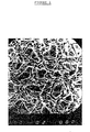
- Figure 1 is an electron micrograph showing the appearance of the drilled epoxy laminate after the pre-treatment step of method A.
- the downhole topography of the laminate consists of a series of resin islands rich in manganese.
- the pre-treated laminate is then treated with an aqueous acidic solution of an organic monomer such as pyrrole, furane, aniline or thiophene for a period of 1 minute at 25 o C.
- the acidic component is preferably toluene-4-sulphonic acid, but this can be varied.
- the organic monomer and acid components which are used are preferably Fluka reagent grade or laboratory grade BDH reagents.
- the monomer solution may comprise 1-50 g/l of toluene-4-sulphonic acid, 1-25 g/l of sodium toluene-4-sulphonate and 6-25 ml/l of pyrrole, preferably about 10 g/l, 10 g/l and 15 ml/l respectively.
- the pH of the resulting solution should be about 2.
- the organic monomer in the solution polymerises in the presence of the acid and the oxidising agent adsorbed on the laminate surface to form a film of a conductive organic polymer on the hole-wall surface.
- the film coated laminate board is then dried at room temperature for 1 minute, after which it is subjected to conventional electroplating using e.g. an acid copper bath containing CuSO4.5H2O (75 g/l), H2SO4 (120 ml/l), Copper Gleam 2000 Additive (obtainable from LeaRonal) and a carrier.
- the electroplating time is dependent upon the aspect ratio of the board. For an 8:1 board, electroplating is carried out for 15 minutes at 1 Adm ⁇ 2 and then 60 minutes at 3 Adm ⁇ 2.
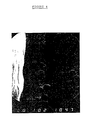
- Figure 2 is an electron micrograph showing the binding action of copper around the epoxy islands after treatment with pyrrole using method A.
- a through-hole epoxy laminate board is again subjected to pre-treatment using a conditioner and an oxidiser.
- the conditioning treatment is carried out for 4 minutes at 65 o C and the oxidising treatment is carried out for 10 minutes at 80 o C.
- the epoxy laminate is subjected to rinsing for 2 minutes at 25 o C after each of these steps.
- the laminate is then subjected to neutralisation at 55 o C for 5 minutes followed by rinsing at 25 o C for 2 minutes.
- the neutralisation can be carried out for example in an aqueous solution of hydrazine hydrate including EDTA having a pH adjusted to about 7.
- EDTA a pH adjusted to about 7.
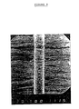
- manganese rich resin islands present after the oxidation step are removed and the resin is left with a micro-rough honeycomb appearance as illustrated in Figure 3.
- the resin has a white appearance and is devoid of manganese.
- Such a micro-rough topography promotes good bonding between the hole-wall and metallised layer deposited later.
- the laminate is then subjected to re-oxidation at 80 o C for 5 minutes using permanganate solution during which permanganate is adsorbed on the hole-wall surface of the laminate.
- the laminate is then subjected to further rinsing at 25 o C for 2 minutes.
- the remaining steps of applying the polymer and electroplating the metal are identical to those set out for method A except that the monomer solution is applied to the re-oxidised laminate for three minutes rather than one minute, and the electroplating is carried out in the case of an 8:1 ratio board for 30 minutes at 1 Adm ⁇ 2 and then for 110 minutes at 3 Adm ⁇ 2.
- the surface to hole ratio obtained using the conducting polymer system of method B shows an improvement in distribution when compared to the conventional electroless copper metallisation process.
- the topography of the micro-rough resin is unaffected by the re-oxidation treatment as illustrated in Figure 4. This was shown by eliminating the conditioning stage from method B, the topography of the resin being scolloped shaped and smooth but high in manganese prior to neutralisation.
- plating tests were carried out using FR4 drilled epoxy laminate obtained from Microtech which have a surface area of 0.5 dm2.
- Thermal shock tests were carried out at 266 o C in solder or glycerol for 0.8 mm and 0.3 mm holes respectively.
- Hole-wall adhesion was graded using a conventional system, and hole-wall coverage was assessed by scanning electron microscopy.
- Circuit board test pieces were metallised in accordance with process A.
- the polymer film was formed by using an aqueous solution comprising pyrrole (0.1 M) and toluene-4-sulphonic acid (0.1M).
- This solution also included nonyl phenyl ethoxylate as a surfactant which reduces the rate of formation of pyrrole black.
- Such a solution may be continuously used without deterioration in coverage or adhesion.
- a polymeric film of polypyrrole having a thickness of 0.1 microns was formed as a black adherent coating on the hole-wall surface of the laminate. Because this black film is conductive, it may be electroplated with an adherent metal layer e.g. copper by electrolytic deposition. The copper is not instantaneously deposited across the entire surface of the conductive polymer film, but rather spreads across the surface apparently by a mechanism of nucleation spread of the copper nuclei across the film. The density of nucleation sites increases with time, and bridging between the nuclei results in the deposited metal layer being substantially pore free.
- Figure 5 is an electron micrograph which illustrates the nucleation spread of copper crystals across the polypyrrole coated epoxy laminate.
- optimised adhesion of the copper layer to the hole-wall surface was obtained when the conditioner and oxidising times were adjusted to about 3 and 15 minutes respectively. These conditions gave an adhesion grade of 80 or greater, with the thickness of the black stained cracked epoxy region being about 6 microns. Reduction of the oxidation immersion time to 5 minutes or less or removal of the conditioner step results in the surface topography being smooth and void of islands and has the effect of reducing the hole-wall adhesion grade to below 65.
- the conductivity of the polymeric film is increased by increasing the organic monomer and/or the acid concentration.
- Optimum adhesion is obtained using a pyrrole concentration of about 15 ml/l, a toluene-4-sulphonic acid concentration of about 10 g/l, and a sodium toluene-4-sulphonate concention of about 10 g/l.
- the adhesion grade is found to be dependent on the age of the conditioner and oxidiser, as well as the concentration of pyrrole in the monomer solution.
- Figures 6 and 7 illustrate how the age of the permanganate oxidiser solution alters the topography of the epoxy laminate. In particular, the population islets become increasingly dense as the permanganate solution ages. Although this may assist in the adhesion properties of the deposit due to an increased binding area being available, contamination of the solution adversely effects the adhesion grade.
- method B produces a superior adhesion grade to method A. This may be because method B causes less resin recession than method A.
- Method B was used in the metallisation of double sided and multi-layer 4:1 aspect ratio boards using the aged replenished solution. Total coverage with adhesion grades of 100 were obtained using the following pre-treatment conditions.
Landscapes
- Engineering & Computer Science (AREA)
- Chemical & Material Sciences (AREA)
- Materials Engineering (AREA)
- Microelectronics & Electronic Packaging (AREA)
- Chemical Kinetics & Catalysis (AREA)
- Electrochemistry (AREA)
- Manufacturing & Machinery (AREA)
- Metallurgy (AREA)
- Organic Chemistry (AREA)
- Manufacturing Of Printed Wiring (AREA)
- Electroplating Methods And Accessories (AREA)
- Printing Elements For Providing Electric Connections Between Printed Circuits (AREA)
- Treatments Of Macromolecular Shaped Articles (AREA)
Applications Claiming Priority (2)
| Application Number | Priority Date | Filing Date | Title |
|---|---|---|---|
| GB9010328A GB2243838A (en) | 1990-05-09 | 1990-05-09 | Process for metallising a through-hole printed circuit board by electroplating |
| GB9010328 | 1990-05-09 |
Publications (2)
| Publication Number | Publication Date |
|---|---|
| EP0457180A2 true EP0457180A2 (de) | 1991-11-21 |
| EP0457180A3 EP0457180A3 (de) | 1991-11-27 |
Family
ID=10675652
Family Applications (1)
| Application Number | Title | Priority Date | Filing Date |
|---|---|---|---|
| EP19910107477 Withdrawn EP0457180A3 (de) | 1990-05-09 | 1991-05-08 | Metallisierungsverfahren von einer Leiterplatte mit Durchgangbohrungen |
Country Status (3)
| Country | Link |
|---|---|
| US (1) | US5106473A (de) |
| EP (1) | EP0457180A3 (de) |
| GB (1) | GB2243838A (de) |
Cited By (11)
| Publication number | Priority date | Publication date | Assignee | Title |
|---|---|---|---|---|
| WO1992010924A1 (de) * | 1990-12-15 | 1992-06-25 | Hans Höllmüller Maschinenbau GmbH & Co. | Verfahren zur herstellung von durchkontaktierten leiterplatten oder multilayern |
| WO1993020263A1 (de) * | 1992-03-31 | 1993-10-14 | Atotech Deutschland Gmbh | Verfahren zur metallisierung von nichtleitern, insbesondere von leiterplatten |
| WO1994004591A1 (de) * | 1992-08-20 | 1994-03-03 | Atotech Deutschland Gmbh | Lösung zur beschichtung von nichtleitern mit leitfähigen polymeren und verfahren zu deren metallisierung |
| US6395378B2 (en) | 2000-01-14 | 2002-05-28 | Telefonaktiebolaget Lm Ericsson | PCB and method for making PCB with thin copper layer |
| DE10124631C1 (de) * | 2001-05-18 | 2002-11-21 | Atotech Deutschland Gmbh | Verfahren zum direkten elektrolytischen Metallisieren von elektrisch nichtleiteitenden Substratoberflächen |
| WO2003007687A3 (en) * | 2001-07-20 | 2003-12-24 | Univ New York State Res Found | Polymer-matrix materials and methods for making same |
| EP2447296A1 (de) * | 2010-10-29 | 2012-05-02 | Enthone, Inc. | Zusammensetzung und Verfahren zur Ablagerung von leitfähigen Polymeren auf dielektrischen Substraten |
| EP2602357A1 (de) | 2011-12-05 | 2013-06-12 | Atotech Deutschland GmbH | Neuartiges Haftmittel zur Metallisierung von Substratoberflächen |
| EP2645830A1 (de) * | 2012-03-29 | 2013-10-02 | Atotech Deutschland GmbH | Herstellungsverfahren für Schaltungen mit feinen Linien |
| EP2644744A1 (de) | 2012-03-29 | 2013-10-02 | Atotech Deutschland GmbH | Verfahren zur Förderung der Haftung zwischen dielektrischen Substraten und Metallschichten |
| WO2019013179A1 (ja) * | 2017-07-11 | 2019-01-17 | 出光興産株式会社 | 無電解めっき下地膜形成用組成物 |
Families Citing this family (13)
| Publication number | Priority date | Publication date | Assignee | Title |
|---|---|---|---|---|
| US5183552A (en) * | 1989-09-14 | 1993-02-02 | Schering Aktiengesellschaft | Process for metallization of a nonconductor surface, especially on a circuit board having preexisting copper surfaces |
| US5368717A (en) * | 1990-11-26 | 1994-11-29 | The Regents Of The University Of California, Office Of Technology Transfer | Metallization of electronic insulators |
| GB2273063B (en) * | 1992-12-07 | 1997-07-09 | Hailin Ge | Process for treating natural products |
| US5415762A (en) * | 1993-08-18 | 1995-05-16 | Shipley Company Inc. | Electroplating process and composition |
| DE4412463C3 (de) * | 1994-04-08 | 2000-02-10 | Atotech Deutschland Gmbh | Verfahren zur Herstellung einer Palladium-Kolloid-Lösung und ihre Verwendung |
| JP3290295B2 (ja) * | 1994-05-13 | 2002-06-10 | 太陽インキ製造株式会社 | 硬化性樹脂組成物並びに該組成物を用いた多層プリント配線板及びその製造方法 |
| JPH07328050A (ja) * | 1994-06-10 | 1995-12-19 | Siegel:Kk | 整姿用パッド並びにその製造方法 |
| US6210537B1 (en) * | 1995-06-19 | 2001-04-03 | Lynntech, Inc. | Method of forming electronically conducting polymers on conducting and nonconducting substrates |
| US5545308A (en) * | 1995-06-19 | 1996-08-13 | Lynntech, Inc. | Method of using conductive polymers to manufacture printed circuit boards |
| FR2737507B1 (fr) * | 1995-08-04 | 1997-09-26 | Scps | Structures poreuses complexes metallisees ou metalliques, premetallisees par depot d'un polymere conducteur |
| CN101134119A (zh) * | 2002-05-24 | 2008-03-05 | 血管技术国际股份公司 | 用于涂覆医用植入物的组合物和方法 |
| US6745398B1 (en) * | 2003-06-06 | 2004-06-08 | James A. Hennessey | Safety pants with removable knee pads |
| US7063762B2 (en) * | 2003-08-20 | 2006-06-20 | Endicott Interconnect Technologies, Inc. | Circuitized substrate and method of making same |
Family Cites Families (7)
| Publication number | Priority date | Publication date | Assignee | Title |
|---|---|---|---|---|
| US4619741A (en) * | 1985-04-11 | 1986-10-28 | Olin Hunt Specialty Products Inc. | Process for preparing a non-conductive substrate for electroplating |
| EP0206133B1 (de) * | 1985-06-12 | 1991-07-31 | BASF Aktiengesellschaft | Verwendung von Polypyrrol zur Abscheidung von metallischem Kupfer auf elektrisch nichtleitende Materialen |
| JP2575672B2 (ja) * | 1986-11-14 | 1997-01-29 | 清蔵 宮田 | 非導電性物質のメツキ法 |
| US4810333A (en) * | 1987-12-14 | 1989-03-07 | Shipley Company Inc. | Electroplating process |
| ATE111294T1 (de) * | 1988-03-03 | 1994-09-15 | Blasberg Oberflaechentech | Gedruckte schaltplatte mit metallisierten löchern und deren herstellung. |
| DE3887989T2 (de) * | 1988-04-25 | 1994-07-14 | Macdermid Inc | Verfahren zur herstellung von gedruckten schaltungen mit durchgehenden löchern für metallisierung. |
| DE3939676C2 (de) * | 1989-11-28 | 1994-01-27 | Schering Ag | Metallisierung von Nichtleitern |
-
1990
- 1990-05-09 GB GB9010328A patent/GB2243838A/en not_active Withdrawn
-
1991
- 1991-05-03 US US07/695,473 patent/US5106473A/en not_active Expired - Lifetime
- 1991-05-08 EP EP19910107477 patent/EP0457180A3/de not_active Withdrawn
Cited By (26)
| Publication number | Priority date | Publication date | Assignee | Title |
|---|---|---|---|---|
| WO1992010924A1 (de) * | 1990-12-15 | 1992-06-25 | Hans Höllmüller Maschinenbau GmbH & Co. | Verfahren zur herstellung von durchkontaktierten leiterplatten oder multilayern |
| WO1993020263A1 (de) * | 1992-03-31 | 1993-10-14 | Atotech Deutschland Gmbh | Verfahren zur metallisierung von nichtleitern, insbesondere von leiterplatten |
| WO1994004591A1 (de) * | 1992-08-20 | 1994-03-03 | Atotech Deutschland Gmbh | Lösung zur beschichtung von nichtleitern mit leitfähigen polymeren und verfahren zu deren metallisierung |
| DE4227836A1 (de) * | 1992-08-20 | 1994-05-05 | Atotech Deutschland Gmbh | Verfahren zur Metallisierung von Nichtleitern und die Verwendung einer sauren Lösung |
| US5597471A (en) * | 1992-08-20 | 1997-01-28 | Atotech Deutschland Gmbh | Solution for coating non-conductors with conductive polymers and their metallization process |
| US6395378B2 (en) | 2000-01-14 | 2002-05-28 | Telefonaktiebolaget Lm Ericsson | PCB and method for making PCB with thin copper layer |
| DE10124631C1 (de) * | 2001-05-18 | 2002-11-21 | Atotech Deutschland Gmbh | Verfahren zum direkten elektrolytischen Metallisieren von elektrisch nichtleiteitenden Substratoberflächen |
| WO2002095091A3 (en) * | 2001-05-18 | 2003-11-13 | Atotech Deutschland Gmbh | Direct electrolytic metallization of non-conducting substrates |
| US7025867B2 (en) | 2001-05-18 | 2006-04-11 | Atotech Deutschland Gmbh | Direct electrolytic metallization on non-conducting substrates |
| CN1329557C (zh) * | 2001-05-18 | 2007-08-01 | 埃托特克德国有限公司 | 非导电基底的直接电解镀金属 |
| KR100863161B1 (ko) * | 2001-05-18 | 2008-10-13 | 아토테크더치랜드게엠베하 | 비전도성 기판의 직접 전기분해 금속화 방법 |
| WO2003007687A3 (en) * | 2001-07-20 | 2003-12-24 | Univ New York State Res Found | Polymer-matrix materials and methods for making same |
| EP2447296A1 (de) * | 2010-10-29 | 2012-05-02 | Enthone, Inc. | Zusammensetzung und Verfahren zur Ablagerung von leitfähigen Polymeren auf dielektrischen Substraten |
| WO2012058681A3 (en) * | 2010-10-29 | 2012-08-02 | Enthone Inc. | Composition and method for the deposition of conductive polymers on dielectric substrates |
| EP3502159A1 (de) * | 2010-10-29 | 2019-06-26 | MacDermid Enthone Inc. | Zusammensetzung und verfahren zur ablagerung von leitfähigen polymeren auf dielektrischen substraten |
| CN103354818B (zh) * | 2010-10-29 | 2016-10-19 | 恩索恩公司 | 用于在介电基板上沉积导电聚合物的组合物和方法 |
| CN103354818A (zh) * | 2010-10-29 | 2013-10-16 | 恩索恩公司 | 用于在介电基板上沉积导电聚合物的组合物和方法 |
| EP2602357A1 (de) | 2011-12-05 | 2013-06-12 | Atotech Deutschland GmbH | Neuartiges Haftmittel zur Metallisierung von Substratoberflächen |
| WO2013083600A2 (en) | 2011-12-05 | 2013-06-13 | Atotech Deutschland Gmbh | Novel adhesion promoting agents for metallization of substrate surfaces |
| WO2013143961A1 (en) | 2012-03-29 | 2013-10-03 | Atotech Deutschland Gmbh | Method for promoting adhesion between dielectric substrates and metal layers |
| WO2013143732A1 (en) * | 2012-03-29 | 2013-10-03 | Atotech Deutschland Gmbh | Method for manufacture of fine line circuitry |
| EP2644744A1 (de) | 2012-03-29 | 2013-10-02 | Atotech Deutschland GmbH | Verfahren zur Förderung der Haftung zwischen dielektrischen Substraten und Metallschichten |
| EP2645830A1 (de) * | 2012-03-29 | 2013-10-02 | Atotech Deutschland GmbH | Herstellungsverfahren für Schaltungen mit feinen Linien |
| WO2019013179A1 (ja) * | 2017-07-11 | 2019-01-17 | 出光興産株式会社 | 無電解めっき下地膜形成用組成物 |
| JPWO2019013179A1 (ja) * | 2017-07-11 | 2020-05-21 | 出光興産株式会社 | 無電解めっき下地膜形成用組成物 |
| US11421115B2 (en) | 2017-07-11 | 2022-08-23 | Idemitsu Kosan Co., Ltd. | Composition for electroless plating underlying membrane |
Also Published As
| Publication number | Publication date |
|---|---|
| EP0457180A3 (de) | 1991-11-27 |
| GB2243838A (en) | 1991-11-13 |
| GB9010328D0 (en) | 1990-06-27 |
| US5106473A (en) | 1992-04-21 |
Similar Documents
| Publication | Publication Date | Title |
|---|---|---|
| US5106473A (en) | Process for metallizing a through-hole board | |
| JP2657423B2 (ja) | 新規なスルーホールめっき印刷回路基板およびその製造方法 | |
| US5373629A (en) | Through-hole plate printed circuit board with resist and process for manufacturing same | |
| KR100294040B1 (ko) | 2층및다층인쇄회로판의관통-홀도금방법_ | |
| KR100541893B1 (ko) | 금속으로 기판을 코팅하는 방법 | |
| US4919768A (en) | Electroplating process | |
| US20050199587A1 (en) | Non-chrome plating on plastic | |
| JPH0327587A (ja) | スルーホールの壁面に直接電気めっきを行なう方法 | |
| EP0538006A1 (de) | Direkt-Metallisierungsverfahren | |
| US5616230A (en) | Method for direct-electroplating an electrically nonconductive substrate | |
| US4913768A (en) | Process for producing electrical conductor boards | |
| JPH05287582A (ja) | 非導電性材料表面に電気メッキ層を直接形成する方法 | |
| US6632344B1 (en) | Conductive oxide coating process | |
| US4728560A (en) | Electrical printed circuit boards | |
| US5213840A (en) | Method for improving adhesion to polymide surfaces | |
| US4457951A (en) | Etch solution and method | |
| JP2008255460A (ja) | ポリイミド樹脂の無電解めっき処理方法 | |
| CA1162354A (en) | Process for electroless metal plating of a polysulfone substrate | |
| EP0454929A2 (de) | Verfahren zur Verbesserung der Metalladhäsion an Polyimidoberflächen | |
| Chiang et al. | Research on applying direct plating to additive process for printed circuit board | |
| JPH0426794B2 (de) | ||
| KR820001689B1 (ko) | 전기도금 방법으로 동포일을 제조하는 방법 | |
| JPH05308189A (ja) | スルーホールめっき回路基板とその製造方法 | |
| KR820001688B1 (ko) | 전기도금방법에 의한 동포일의 제조방법 | |
| JPH04187781A (ja) | 無電解めっき法 |
Legal Events
| Date | Code | Title | Description |
|---|---|---|---|
| PUAI | Public reference made under article 153(3) epc to a published international application that has entered the european phase |
Free format text: ORIGINAL CODE: 0009012 |
|
| PUAL | Search report despatched |
Free format text: ORIGINAL CODE: 0009013 |
|
| AK | Designated contracting states |
Kind code of ref document: A2 Designated state(s): BE CH DE FR GB LI NL |
|
| AK | Designated contracting states |
Kind code of ref document: A3 Designated state(s): BE CH DE FR GB LI NL |
|
| STAA | Information on the status of an ep patent application or granted ep patent |
Free format text: STATUS: THE APPLICATION IS DEEMED TO BE WITHDRAWN |
|
| 18D | Application deemed to be withdrawn |
Effective date: 19920528 |