EP0457468A2 - Assemblage électronique intégré comprenant une ligne de transmission - Google Patents
Assemblage électronique intégré comprenant une ligne de transmission Download PDFInfo
- Publication number
- EP0457468A2 EP0457468A2 EP91304012A EP91304012A EP0457468A2 EP 0457468 A2 EP0457468 A2 EP 0457468A2 EP 91304012 A EP91304012 A EP 91304012A EP 91304012 A EP91304012 A EP 91304012A EP 0457468 A2 EP0457468 A2 EP 0457468A2
- Authority
- EP
- European Patent Office
- Prior art keywords
- assembly
- major surface
- insulating material
- transmission line
- semiconductor substrate
- Prior art date
- Legal status (The legal status is an assumption and is not a legal conclusion. Google has not performed a legal analysis and makes no representation as to the accuracy of the status listed.)
- Ceased
Links
Images


Classifications
-
- H—ELECTRICITY
- H10—SEMICONDUCTOR DEVICES; ELECTRIC SOLID-STATE DEVICES NOT OTHERWISE PROVIDED FOR
- H10W—GENERIC PACKAGES, INTERCONNECTIONS, CONNECTORS OR OTHER CONSTRUCTIONAL DETAILS OF DEVICES COVERED BY CLASS H10
- H10W20/00—Interconnections in chips, wafers or substrates
- H10W20/40—Interconnections external to wafers or substrates, e.g. back-end-of-line [BEOL] metallisations or vias connecting to gate electrodes
- H10W20/41—Interconnections external to wafers or substrates, e.g. back-end-of-line [BEOL] metallisations or vias connecting to gate electrodes characterised by their conductive parts
- H10W20/44—Conductive materials thereof
- H10W20/4484—Superconducting materials
-
- H—ELECTRICITY
- H10—SEMICONDUCTOR DEVICES; ELECTRIC SOLID-STATE DEVICES NOT OTHERWISE PROVIDED FOR
- H10W—GENERIC PACKAGES, INTERCONNECTIONS, CONNECTORS OR OTHER CONSTRUCTIONAL DETAILS OF DEVICES COVERED BY CLASS H10
- H10W20/00—Interconnections in chips, wafers or substrates
- H10W20/40—Interconnections external to wafers or substrates, e.g. back-end-of-line [BEOL] metallisations or vias connecting to gate electrodes
- H10W20/41—Interconnections external to wafers or substrates, e.g. back-end-of-line [BEOL] metallisations or vias connecting to gate electrodes characterised by their conductive parts
- H10W20/43—Layouts of interconnections
- H10W20/432—Layouts of interconnections comprising crossing interconnections
-
- Y—GENERAL TAGGING OF NEW TECHNOLOGICAL DEVELOPMENTS; GENERAL TAGGING OF CROSS-SECTIONAL TECHNOLOGIES SPANNING OVER SEVERAL SECTIONS OF THE IPC; TECHNICAL SUBJECTS COVERED BY FORMER USPC CROSS-REFERENCE ART COLLECTIONS [XRACs] AND DIGESTS
- Y10—TECHNICAL SUBJECTS COVERED BY FORMER USPC
- Y10S—TECHNICAL SUBJECTS COVERED BY FORMER USPC CROSS-REFERENCE ART COLLECTIONS [XRACs] AND DIGESTS
- Y10S505/00—Superconductor technology: apparatus, material, process
- Y10S505/70—High TC, above 30 k, superconducting device, article, or structured stock
- Y10S505/701—Coated or thin film device, i.e. active or passive
- Y10S505/703—Microelectronic device with superconducting conduction line
-
- Y—GENERAL TAGGING OF NEW TECHNOLOGICAL DEVELOPMENTS; GENERAL TAGGING OF CROSS-SECTIONAL TECHNOLOGIES SPANNING OVER SEVERAL SECTIONS OF THE IPC; TECHNICAL SUBJECTS COVERED BY FORMER USPC CROSS-REFERENCE ART COLLECTIONS [XRACs] AND DIGESTS
- Y10—TECHNICAL SUBJECTS COVERED BY FORMER USPC
- Y10S—TECHNICAL SUBJECTS COVERED BY FORMER USPC CROSS-REFERENCE ART COLLECTIONS [XRACs] AND DIGESTS
- Y10S505/00—Superconductor technology: apparatus, material, process
- Y10S505/825—Apparatus per se, device per se, or process of making or operating same
- Y10S505/873—Active solid-state device
Definitions
- This invention pertains to integrated electronic assemblies, typically semiconductor ICs. More particularly, it pertains to such assemblies that comprise means for conducting an electrical signal from one part of the assembly to another part thereof.
- Electrical signals are conventionally propagated from one part of a given semiconductor IC chip to another part thereof by means of metal lines on an insulator, the latter in turn typically being in contact with (and supported by) insulator on semiconductor material. Signal propagation on such conventional lines is relatively slow, due at least in part to the relatively high dielectric constant of semiconductor material.
- a 50 Gbit/sec data rate exemplarily requires a 50 GHz clock signal and its complement, which can be distributed less than 1 mm (using metal lines on GaAs) before timing errors between devices become important.
- a further important aspect of high frequency intra-chip signal transmission is dispersion, especially dispersion associated with the presence of higher order modes. It is known that higher order modes in microstrip lines typically are strongly associated not with the conductive strip but with the dielectric-air interface. See, for instance, Microstrip Lines and Slotlines , K. C. Gupta et al., Artech House, Inc., Washington 1979, p. 65.
- Waveguides comprising a conductor strip supported within a conductive housing are known. See, for instance, F. Alessandri et al., IEEE Transactions on Microwave Theory and Techniques , Vol. 37(12), pp. 2020-2027. See also S. Loualiche et al., Electronics Letters , Vol. 26(4), pp. 266-267, wherein is disclosed a non-integrated microwave assembly that comprises an air gap stripline on a InP substrate.
- waveguides clearly can not be produced by conventional semiconductor manufacturing techniques and can not readily be integrated into a semiconductor IC chip. They thus are not suitable as intrachip conductors.
- intra-chip conductor means that support signal propagation speeds substantially in excess of those associated with conventional prior art conductors, that are substantially free of dielectric discontinuity, and that preferably are of a geometry that is relatively free of field lines that cross an air-dielectric interface, such that generation of higher order modes is relatively low.
- This application discloses such assemblies.
- the invention is an integrated electronic assembly (typically a semiconductor IC chip) that comprises conductive means adapted for relatively high speed, low dispersion transmission of electrical signals.
- relatively high speed we mean a signal propagation speed that is substantially (at least 25%, preferably 50% or even 100%) higher than that obtainable with analogous prior art conductor means.
- the signal propagation speed is at least about c/2, where c is the speed of light in vacuum.
- an exemplary electronic assembly comprises a semiconductor substrate, insulating material and conductive means that signal-transmissively connect a first region (exemplarily a device such as a transistor) to a second region (exemplarily also a transistor, or input or output contact means) of the assembly.
- the conductive means comprise an elongate conductive body, exemplarily one (or possibly two parallel) metal lines. Typically the length of the elongate conductive body is at least about 100 ⁇ m, and can be one to several millimeters.
- the insulating material is disposed such that the elongate conductive body is spaced apart from the semiconductor substrate.
- the body is in contact with (and typically supported by) insulating material (e.g., SiO2), and the insulating material in turn is in contact with (and typically supported by) the semiconductor substrate.
- insulating material e.g., SiO2
- the semiconductor substrate Associated with the semiconductor substrate is a dielectric constant (whose value is readily available from a variety of sources), and associated with the conductive means is a length and an effective dielectric constant (whose value can, at least in principle, be calculated by known techniques).
- the semiconductor substrate comprises one or more recesses that are configured such that at least a portion of the insulating material (with the conductive means thereon) is spaced apart from the semiconductor substrate, such that the effective dielectric constant associated with at least a major portion of the length of the conductive means is substantially lower than the effective dielectric constant associated with an otherwise identical comparison assembly which does not comprise said recesses, and is furthermore substantially uniform over the portion.
- a “major portion” of the length of the conductive means we mean at least 50% of the total length of the conductor connecting the first and second regions of the electronic assembly.
- FIG. 1 schematically depicts in cross section a co-planar transmission line which exhibits high signal speed.
- a co-planar transmission line we mean herein a transmission line having at least one conductor substantially at the level of the "front" surface of the semiconductor body.
- semiconductor substrate 10 e.g., semi-insulating InP
- two substantially parallel gold conductor lines 120 and 121 e.g., 10 ⁇ m width, 1 ⁇ m thickness, 10 ⁇ m spacing.
- Such lines can readily be formed by conventional means.
- the substrate surface is etched in HCl, such that recesses 110, 111 and 112 (exemplarily 7 ⁇ m deep) are formed.
- the substrate portions that support the conductor lines are about 3 ⁇ m thick. This latter dimension is relatively difficult to control reliably.
- FIG. 3 shows schematically a particular embodiment of the inventive transmission line, wherein numeral 30 refers to the semiconductor substrate (e.g., semi-insulating GaAs), numerals 310 and 311 to insulator material (e.g., 200 nm thick SiO2), and numerals 320 and 321 to (co-planar) conductor lines (e.g., 1 ⁇ m thick and 5 ⁇ m wide Au lines).
- the gap between the conductors exemplarily is about 5 ⁇ m.
- Recess 33 can be produced by known means, e.g., by etching for 5 minutes in H2O2: H2SO4: 40H2O.
- the insulator material both acts as an etch mask and as support for the conductor lines.
- FIG. 3 shows only the relevant portion of an integrated electronic assembly according to the invention.
- Other portions can be conventional and are not shown.
- the latter typically will be relatively short, exemplarily less than about 100 ⁇ m, if the inventive assembly is adapted for high frequency (e.g., at least 10 GHz, possibly more than 50 GHz) operation.
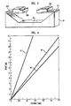
- FIG. 4 shows exemplary data on pulse delay versus propagation distance, with line 40 pertaining to an inventive transmission line according to FIG. 3, line 41 to an (otherwise identical) unetched comparison transmission line, and line 42 represents the speed of light (c).
- Lines 40 and 41 correspond to propagation velocities of 0.86c and 0.39c, respectively.
- the inventive transmission line thus has a propagation speed more than twice that of the (unetched) comparison line.
- the propagation speed of the unetched line is approximately is the effective dielectric constant associated with the unetched transmission line, with ⁇ being the static dielectric constant of the semiconductor (12.85 for GaAs), and ⁇ o being the dielectric constant of vacuum (and air), namely 1. For a GaAs substrate this gives a propagation speed of 0.38c, in good agreement with the measured propagation speed.
- ⁇ av of the inventive transmission line of FIGs. 3 and 4 is 1.35.
- the effective dielectric constant associated with the exemplary inventive transmission line clearly is much less than the dielectric constant of the unetched comparison line.
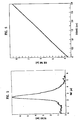
- FIG. 5 shows a test pulse after 75 ⁇ m of propagation
- FIG. 6 shows the pulse rise time as a function of propagation distance. The data shows that a pulse having initial risetime of 0.37ps still has only 0.8ps risetime after 3 mm propagation, indicative of low dispersion.
- FIG. 7 schematically shows a transmission line according to the invention that comprises a semiconductor (e.g., Si) substrate 70 with a recess 73 therein, with conductor lines 710 and 711 supported (and partially overlain) by insulators 720 and 721, respectively.
- the insulators can comprise "windows" (not shown) that can serve to improve etching of the recess.
- FIG. 8 A further exemplary geometry is schematically shown in FIG. 8, wherein recess 83 extends from the "back" of substrate 80 to the transmission line.
- FIG. 9 A still further exemplary geometry is schematically depicted in FIG. 9.
- This embodiment comprises a conductive backplane 91 on substrate 90, with recess 95 optionally extending completely through the substrate.
- Single conductor 92 is supported by insulator layer 93.
- "Windows" 940 and 941 in 93 permit etch access.
- an axial strip is opened through 93, with 92 extending over the opened strip.
- FIG. 10 shows a still further exemplary geometry, wherein recess 101 extends only part-way through semiconductor substrate 100, with conductor 102 forming the bottom electrode of the transmission line.
- the bottom electrode can, for instance, be formed by angle evaporation through the "windows" in the insulator layer 93, as will be apparent to those skilled in the art.
- the invention is not limited to metal conductor bodies, and that any other material of acceptable conductivity [including metal silicide, as well as “low T c " and “high T c “ (e.g., YBa2Cu3O7) superconductor] can be used in the practice of the invention.
- the invention is not limited to the use of a semiconductor substrate.
- SrTiO3 is an advantageous substrate for YBa2Cu3O7 films, and high T c superconductor co-planar air gap transmission lines on metal oxide substrates, or on an oxide buffer layer on a semiconductor substrate, are contemplated.
Landscapes
- Internal Circuitry In Semiconductor Integrated Circuit Devices (AREA)
- Semiconductor Integrated Circuits (AREA)
- Containers, Films, And Cooling For Superconductive Devices (AREA)
- Waveguides (AREA)
Applications Claiming Priority (2)
| Application Number | Priority Date | Filing Date | Title |
|---|---|---|---|
| US523093 | 1990-05-14 | ||
| US07/523,093 US5012319A (en) | 1990-05-14 | 1990-05-14 | Integrated electronic assembly comprising a transmission line |
Publications (2)
| Publication Number | Publication Date |
|---|---|
| EP0457468A2 true EP0457468A2 (fr) | 1991-11-21 |
| EP0457468A3 EP0457468A3 (en) | 1992-04-08 |
Family
ID=24083630
Family Applications (1)
| Application Number | Title | Priority Date | Filing Date |
|---|---|---|---|
| EP19910304012 Ceased EP0457468A3 (en) | 1990-05-14 | 1991-05-03 | Integrated electronic assembly comprising a transmission line |
Country Status (3)
| Country | Link |
|---|---|
| US (1) | US5012319A (fr) |
| EP (1) | EP0457468A3 (fr) |
| JP (1) | JPH04230104A (fr) |
Cited By (1)
| Publication number | Priority date | Publication date | Assignee | Title |
|---|---|---|---|---|
| WO1994005046A3 (fr) * | 1992-08-24 | 1994-06-09 | Conductus Inc | Structures autonomes en materiaux a base d'oxyde du type perovskite |
Families Citing this family (7)
| Publication number | Priority date | Publication date | Assignee | Title |
|---|---|---|---|---|
| EP0811257A4 (fr) * | 1995-02-23 | 1998-04-29 | Superconductor Tech | Procede et appareil pour augmenter la tenue en puissance de dispositifs supraconducteurs pour hautes temperatures |
| CA2148341C (fr) * | 1995-05-01 | 1997-02-04 | Shen Ye | Methode et structure utilisant des rubans separes par un espace pour lignes de transmission haute tension a supraconducteur a haute temperature |
| JP3218996B2 (ja) * | 1996-11-28 | 2001-10-15 | 松下電器産業株式会社 | ミリ波導波路 |
| US5949312A (en) * | 1997-10-30 | 1999-09-07 | Motorola, Inc. | Suspended monolithic microwave integrated circuit and method of manufacture |
| JP2000156621A (ja) | 1998-11-19 | 2000-06-06 | Philips Japan Ltd | 高周波誘電体装置 |
| JP4823541B2 (ja) * | 2005-03-18 | 2011-11-24 | 富士通セミコンダクター株式会社 | 高周波伝送線路 |
| CN115842227A (zh) * | 2021-09-22 | 2023-03-24 | 康普技术有限责任公司 | 移相器及其制造方法 |
Family Cites Families (7)
| Publication number | Priority date | Publication date | Assignee | Title |
|---|---|---|---|---|
| JPS4834686A (fr) * | 1971-09-09 | 1973-05-21 | ||
| JPS5619636A (en) * | 1979-07-26 | 1981-02-24 | Nec Corp | Integrated circuit semiconductor device |
| US4379307A (en) * | 1980-06-16 | 1983-04-05 | Rockwell International Corporation | Integrated circuit chip transmission line |
| JPS62250657A (ja) * | 1986-04-23 | 1987-10-31 | Nec Corp | 半導体集積回路 |
| JPH01183138A (ja) * | 1988-01-18 | 1989-07-20 | Fujitsu Ltd | 半導体装置 |
| JPH0276402A (ja) * | 1988-09-13 | 1990-03-15 | Nec Corp | 超伝導遅延装置 |
| EP0393635B1 (fr) * | 1989-04-21 | 1997-09-03 | Nec Corporation | Dispositif semi-conducteur comprenant des conducteurs multicouche |
-
1990
- 1990-05-14 US US07/523,093 patent/US5012319A/en not_active Expired - Lifetime
-
1991
- 1991-05-01 JP JP3126442A patent/JPH04230104A/ja active Pending
- 1991-05-03 EP EP19910304012 patent/EP0457468A3/en not_active Ceased
Cited By (1)
| Publication number | Priority date | Publication date | Assignee | Title |
|---|---|---|---|---|
| WO1994005046A3 (fr) * | 1992-08-24 | 1994-06-09 | Conductus Inc | Structures autonomes en materiaux a base d'oxyde du type perovskite |
Also Published As
| Publication number | Publication date |
|---|---|
| JPH04230104A (ja) | 1992-08-19 |
| EP0457468A3 (en) | 1992-04-08 |
| US5012319A (en) | 1991-04-30 |
Similar Documents
| Publication | Publication Date | Title |
|---|---|---|
| US5387547A (en) | Process for adjusting the impedance of a microwave conductor using an air bridge | |
| US4906953A (en) | Broadband microstrip to coplanar waveguide transition by anisotropic etching of gallium arsenide | |
| US4626805A (en) | Surface mountable microwave IC package | |
| US7101778B2 (en) | Transmission lines for CMOS integrated circuits | |
| JP3241139B2 (ja) | フィルムキャリア信号伝送線路 | |
| US4837536A (en) | Monolithic microwave integrated circuit device using high temperature superconductive material | |
| US7869242B2 (en) | Transmission lines for CMOS integrated circuits | |
| JPS5821901A (ja) | 回路整合素子 | |
| US5008639A (en) | Coupler circuit | |
| US5012319A (en) | Integrated electronic assembly comprising a transmission line | |
| US4996582A (en) | Field effect transistor for microstrip mounting and microstrip-mounted transistor assembly | |
| JPH10200311A (ja) | 裏面接地導体付きコプレーナウエーブガイド線路 | |
| KR100300235B1 (ko) | 반도체의입출력접속구조 | |
| KR100339373B1 (ko) | 마이크로스트립카플러및그의제조방법 | |
| KR100297216B1 (ko) | 반도체장치 | |
| US6490379B2 (en) | Electrical transmission frequency of SiOB | |
| US5493263A (en) | Microstrip which is able to supply DC bias current | |
| US4644093A (en) | Circuit board | |
| EP0321065A3 (fr) | Procédé de fabrication de dispositifs semi-conducteurs composites du type Schottky | |
| JPS59124172A (ja) | Fet製造方法 | |
| EP0117335A1 (fr) | Photodiodes à grande vitesse de commutation | |
| US4692720A (en) | Arrangement for producing a junction between a microstrip line and a coplanar transmission line | |
| IE54372B1 (en) | Semiconductor device having conductor lines connecting the elements | |
| KR940011024B1 (ko) | 초고주파수 대역용 고전력 증폭기 | |
| US6919773B2 (en) | Monolithically integrated microwave guide component for radio frequency overcoupling |
Legal Events
| Date | Code | Title | Description |
|---|---|---|---|
| PUAI | Public reference made under article 153(3) epc to a published international application that has entered the european phase |
Free format text: ORIGINAL CODE: 0009012 |
|
| AK | Designated contracting states |
Kind code of ref document: A2 Designated state(s): DE FR GB |
|
| PUAL | Search report despatched |
Free format text: ORIGINAL CODE: 0009013 |
|
| AK | Designated contracting states |
Kind code of ref document: A3 Designated state(s): DE FR GB |
|
| 17P | Request for examination filed |
Effective date: 19920925 |
|
| RAP3 | Party data changed (applicant data changed or rights of an application transferred) |
Owner name: AT&T CORP. |
|
| 17Q | First examination report despatched |
Effective date: 19940808 |
|
| GRAG | Despatch of communication of intention to grant |
Free format text: ORIGINAL CODE: EPIDOS AGRA |
|
| STAA | Information on the status of an ep patent application or granted ep patent |
Free format text: STATUS: THE APPLICATION HAS BEEN REFUSED |
|
| 18R | Application refused |
Effective date: 20000104 |