EP0457626B1 - Procédé et dispositif pour la division en tranches d'un lingot monocristallin au moyen d'une scie annulaire - Google Patents
Procédé et dispositif pour la division en tranches d'un lingot monocristallin au moyen d'une scie annulaire Download PDFInfo
- Publication number
- EP0457626B1 EP0457626B1 EP91304540A EP91304540A EP0457626B1 EP 0457626 B1 EP0457626 B1 EP 0457626B1 EP 91304540 A EP91304540 A EP 91304540A EP 91304540 A EP91304540 A EP 91304540A EP 0457626 B1 EP0457626 B1 EP 0457626B1
- Authority
- EP
- European Patent Office
- Prior art keywords
- rate
- ingot
- feed
- cut
- single crystal
- Prior art date
- Legal status (The legal status is an assumption and is not a legal conclusion. Google has not performed a legal analysis and makes no representation as to the accuracy of the status listed.)
- Expired - Lifetime
Links
Images


Classifications
-
- B—PERFORMING OPERATIONS; TRANSPORTING
- B28—WORKING CEMENT, CLAY, OR STONE
- B28D—WORKING STONE OR STONE-LIKE MATERIALS
- B28D5/00—Fine working of gems, jewels, crystals, e.g. of semiconductor material; apparatus or devices therefor
- B28D5/02—Fine working of gems, jewels, crystals, e.g. of semiconductor material; apparatus or devices therefor by rotary tools, e.g. drills
- B28D5/022—Fine working of gems, jewels, crystals, e.g. of semiconductor material; apparatus or devices therefor by rotary tools, e.g. drills by cutting with discs or wheels
- B28D5/024—Fine working of gems, jewels, crystals, e.g. of semiconductor material; apparatus or devices therefor by rotary tools, e.g. drills by cutting with discs or wheels with the stock carried by a movable support for feeding stock into engagement with the cutting blade, e.g. stock carried by a pivoted arm or a carriage
-
- B—PERFORMING OPERATIONS; TRANSPORTING
- B23—MACHINE TOOLS; METAL-WORKING NOT OTHERWISE PROVIDED FOR
- B23D—PLANING; SLOTTING; SHEARING; BROACHING; SAWING; FILING; SCRAPING; LIKE OPERATIONS FOR WORKING METAL BY REMOVING MATERIAL, NOT OTHERWISE PROVIDED FOR
- B23D59/00—Accessories specially designed for sawing machines or sawing devices
- B23D59/001—Measuring or control devices, e.g. for automatic control of work feed pressure on band saw blade
-
- B—PERFORMING OPERATIONS; TRANSPORTING
- B23—MACHINE TOOLS; METAL-WORKING NOT OTHERWISE PROVIDED FOR
- B23Q—DETAILS, COMPONENTS, OR ACCESSORIES FOR MACHINE TOOLS, e.g. ARRANGEMENTS FOR COPYING OR CONTROLLING; MACHINE TOOLS IN GENERAL CHARACTERISED BY THE CONSTRUCTION OF PARTICULAR DETAILS OR COMPONENTS; COMBINATIONS OR ASSOCIATIONS OF METAL-WORKING MACHINES, NOT DIRECTED TO A PARTICULAR RESULT
- B23Q15/00—Automatic control or regulation of feed movement, cutting velocity or position of tool or work
- B23Q15/007—Automatic control or regulation of feed movement, cutting velocity or position of tool or work while the tool acts upon the workpiece
- B23Q15/013—Control or regulation of feed movement
-
- B—PERFORMING OPERATIONS; TRANSPORTING
- B28—WORKING CEMENT, CLAY, OR STONE
- B28D—WORKING STONE OR STONE-LIKE MATERIALS
- B28D5/00—Fine working of gems, jewels, crystals, e.g. of semiconductor material; apparatus or devices therefor
- B28D5/02—Fine working of gems, jewels, crystals, e.g. of semiconductor material; apparatus or devices therefor by rotary tools, e.g. drills
- B28D5/022—Fine working of gems, jewels, crystals, e.g. of semiconductor material; apparatus or devices therefor by rotary tools, e.g. drills by cutting with discs or wheels
- B28D5/028—Fine working of gems, jewels, crystals, e.g. of semiconductor material; apparatus or devices therefor by rotary tools, e.g. drills by cutting with discs or wheels with a ring blade having an inside cutting edge
Definitions
- the present invention relates to a method of using an ID saw slicing machine for slicing a single crystal ingot in a direction normal to the axis of the ingot to thereby obtain thin wafers, and also to a slicing apparatus for effecting the slicing operation of the method.
- An ID saw slicing machine is a slicing machine equipped with a thin doughnut-shaped blade with the inner edge coated with a hard material such as diamond powder. This machine is particularly useful in slicing a brittle rod such as a single crystal semiconductor ingot.
- a brittle rod such as a single crystal semiconductor ingot.
- a silicon single crystal ingot pulled up in a conventional single crystal pulling apparatus is sliced with an ID saw slicing machine (hereinafter also referred to as "an ID slicer") in a direction normal to the axis of the ingot, and a number of silicon semiconductor wafers are cut out.
- an ID slicer an ID saw slicing machine
- the blade of the ID slicer wears and starts wobbling, and this causes the sliced wafer to show so-called face bow, which is a warp in one direction, or in other words, the residual stress in the wafer causes the wafers to curl slightly.
- some of the commercially available ID slicers are equipped with a displacement gauge which measures the wobble displacement of the blade of the slicer.
- the wobbling of the blade is detected by means of the displacement gauge, and based on the result of the detection, the blade is appropriately dressed and trued; also the slicing rate is modified in response to the result of the detection of the blade displacement in a feedback manner.
- the present invention was made in view of these problems, and it is an object of the invention to provide a method of using an ID saw slicing machine for slicing a single crystal ingot into wafers in which the amount of bow is reduced, and also to provide a slicing apparatus for effecting this method.
- an improved method of using an ID saw slicing machine having a blade which is rotated at a constant high speed for slicing a single crystal ingot in a direction normal to the axis of the ingot to obtain wafers wherein the feed-rate of the single crystal ingot to the blade of the ID saw slicing machine varies with time during the cut (as is known, for example, from US-A-3039235); characterised in that: the feed-rate is alternated repeatedly during the cut between a first minimum rate and a second maximum rate, the variation of said feed-rate between said minimum and maximum rates being controlled in a predetermined cyclic manner, whereby a controlled irregularity is imparted to the surface of the wafer cut from the ingot such that any tendency of the wafer to warp during cutting is reduced.
- apparatus for slicing a single crystal ingot comprising an ID saw slicing machine for slicing a single crystal ingot in a direction normal to the axis of the ingot, a drive means for rotating a blade of the ID saw slicing machine at a constant high speed, shift means for relative translation of the ID saw slicing machine and single crystal ingot such that the ingot is sliced in a direction normal to its axis, and a control means for controlling the shift means (7) so as to vary the feed-rate of the single crystal ingot (6) to the blade (2) of the ID saw slicing machine (1) (as is known, for example, from US-A-3039235); characterised in that: said control means is adapted to alternate the feed-rate repeatedly during the cut between a first minimum rate and a second maximum rate, the variation of said feed-rate between said minimum and maximum rates being controlled in a predetermined cyclic manner, whereby a controlled irregularity is imparted to
- the feed of the single crystal ingot to the blade of the ID slicer is controlled to increase and decrease alternately in accordance with the predetermined program, so that it is possible to intentionally give controlled irregularity to the surface of the wafer sliced from the single crystal ingot.
- the load resistance imposed by the single crystal ingot being sliced increases and causes the blade to wobble more roughly and thus the displacement of the blade is increased, and, on the other hand, when the feed is low, the load resistance decreases and causes the blade to wobble less roughly and thus the displacement of the blade is decreased; as a result, the wafer will easily have an irregular surface.
- the degrees (in magnitude and pitch) of the irregularity can be controlled by modifying the feed control pattern, for example the magnitude of the feed rate, the time pitch between the high rate feed and the low rate feed, and by controlling the operation carefully, the roughness of the irregularity can be restrained to a certain level.
- This intentionally formed irregularity prevents the wafer from warping and thus the resulting wafer will scarcely have a bow.
- the irregularity can be eventually removed by lapping and etching the wafer in the conventional manner. Consequently, it is possible to obtain a wafer with reduced warp or bow.
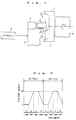
- Reference numeral 1 designates an ID slicer which mainly consists of a thin ring blade 2, a dram-like main spindle head 3, and a motor 4.
- the outer edge of the blade 2 is embedded and fixed in the peripheral portion of the main spindle head 3; the blade 2 is held vertically and in coaxial alignment with the main spindle head 3, which is fixedly supported about the output shaft of the motor 4.
- the inner circumference of the blade 2 is formed with grinder edge 2a consisting of diamond powder.
- a feeder unit 5 which serves as an ingot mount as well.
- a cylindrical silicon single crystal ingot 6 to be sliced and an ingot slider unit 7 are mounted on the feeder unit 5.
- a controller 8 as the control means is electrically connected to the feeder unit 5.
- the ID slicer 1 directly connected to the shaft, is rotated in the same direction at a predetermined rate. Then, the ingot slider unit 7 pushes the single crystal silicon ingot 6 to slide in the direction indicated by the arrow C by a predetermined amount whereby the front end of the ingot 6 crosses across the hole defined by the inner circumference of the blade 2 of the ID slicer 1, as shown in Fig. 1.
- the feeder unit 5 is driven to shift the single crystal ingot 6 together with the ingot slider 7 in the direction indicated by the arrow B of Fig. 1 whereby the single crystal ingot 6 is cut by the grinder edge 2a of the blade 2 in the direction opposite to the arrow B which is normal to the axis of the ingot 6.
- the shifting of the ingot in direction B is continued until a thin disk-shaped silicon semiconductor wafer is completely severed from the ingot 6.
- the feeder unit 5 is driven in the direction opposite to direction B to shift back to the original position; at the same time the ingot slider unit 7 again urges the single crystal ingot 6 to shift in direction C by the predetermined amount so that the front end of the ingot 6 again enters the hole defined by the grinder edge 2a of the blade 2.
- the same procedure as described above is repeated to slice the wafers one after another off the ingot 6.
- the shifting operation of the feeder unit 5 is controlled by the controller 8 in a manner such that the velocity of the feeder unit 5 in direction B, that is, the feed rate of the single crystal ingot 6 is varied in accordance with a predetermined program stored in the controller 8.
- Fig. 2 shows an example of the program in which the feed rate is altered between a high rate and a low rate.
- the first 1-mm segment a is fed and cut at a lower feed rate of 6 mm/min.; during the cutting of the second 1-mm segment b the feed rate is gradually increased from 6 mm/min. to a higher feed rate of 60 mm/min.; during the cutting of the third 1-mm segment c the feed of the ingot 6 is maintained at the higher feed rate of 60 mm/min.; then during the cutting of the fourth 1-mm segment d the feed rate is gradually decreased to the lower rate of 6 mm/min. This feed rate cycle is repeated until a wafer is severed off.
- the load resistance imposed by the single crystal ingot 6 being sliced on the blade 2 becomes greater, and thus the blade 2 wobbles more roughly to increase its displacement.
- the load resistance becomes smaller, and thus the blade 2 wobbles less roughly to thereby decrease its displacement. Consequently, as in the present embodiment, when the feed is controlled to alternate between a high rate and a low rate, the displacement of the blade will increase and decrease between an upper value and a lower value, as observed in the graph of Fig. 3.
- the silicon semiconductor wafer W′ thus severed from the ingot 6 has surfaces with controlled irregularity, as shown at (a) in Fig. 4.
- the irregularity is convexed and at the serpents that are ground at the low feed rate, the irregularity is concaved; thus the wobbling blade 2 causes the semiconductor wafer W′ to have irregular layers W1′ and W2′ at the surfaces.
- the alternating irregularity prevents the wafer from curling, and since the controlled irregularity is not as roughly made as it would be when uncontrolled, the roughness of the irregularity can be restricted to less than a certain degree.
- the both faces of the semiconductor wafer W′ are lapped with loose abrasive grain.
- the convexed portions of the irregularity are first ground off by the lapping stool; then the concaved portions of the irregularity are smoothed as the lapping proceeds.
- the semiconductor wafer W'' is steeped in an etchant such as the mixed acid for a predetermined time period.
- This etching treatment removes the residual rough layers W1'' and W2'' from the faces of the semiconductor wafer W''.
- a semiconductor wafer W having no irregular or rough layers as well as having reduced bow is obtained.
- a number of thus obtained silicon semiconductor wafer having a diameter of 15.24 cm (6 inch) were measured for their bow ( X ) and found to have an average bow ( X ) of 6 ⁇ m with a dispersion ⁇ of 2 ⁇ m. These values are half of those of the semiconductor wafers obtained through the conventional method. Thus the improvement brought about by the present invention is proved.
- Fig. 5 shows the result of the measurement of the surface roughness of a 6-inch semiconductor wafer obtained through the procedure of the present embodiment.
- the axis of abscissa represents the length l of the semiconductor wafer along a certain diameter [ref. l in 9 (c) of Fig. 4]
- the axis of ordinate represents the degree of the surface roughness
- R represents the average surface roughness.
- Fig. 6 shows a chart representing another example of the program for controlling the variation of the feed which is stored in the controller 8 (ref. Fig. 1).
- a dashed-line curve D represents an empirically obtained graph which is characteristic in that if the feed is changed along this curve D while slicing a single crystal ingot the load resistance imposed by the ingot being sliced keeps constant.
- the first 1-mm segment of the ingot is fed at a lower feed rate of 6 mm/min.; during the cutting of the second 1-mm segment the feed rate is continuously increased from 6 mm/min. to a highe feed rate of 80 mm/min.
- the similar cycle is repeated until a wafer is cut off.
- the wafer obtained in this example also has surfaces with controlled irregularity, similar to the one shown at (a) in Fig. 4, and the bow of the wafer is slighter than the that of a conventionally obtained wafer.
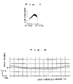
- Fig. 7 shows the displacement of the blade 2
- Fig. 8 shows the surface roughness of the wafer obtained in the present example.
- the slicing of the wafer was effected as the single crystal ingot 6 is moved while the ID saw slicer 1 is kept stationary, it is also possible to effect the slicing by moving the ID saw slicer 1 while the single crystal ingot 6 is kept stationary. In the latter case, the shifting velocity of the body consisting of the ID saw slicer 1 and the motor 4 is controlled by the controller 8.
- the feed of the single crystal ingot to the blade of the ID saw slicing machine is increased and decreased alternately in accordance with a predetermined control pattern, so that it is possible to intentionally give slight irregularity to the faces of the wafer sliced from the single crystal ingot; as a result, the wafer will have slighter bow even after removing the irregularity through conventional lapping and etching processes.
Landscapes
- Engineering & Computer Science (AREA)
- Mechanical Engineering (AREA)
- Processing Of Stones Or Stones Resemblance Materials (AREA)
- Mechanical Treatment Of Semiconductor (AREA)
Claims (5)
- Procédé éprouvé pour la division en tranches d'un lingot monocristallin (6) au moyen d'une scie annulaire (1) comportant une lame (2) qui est entraînée en rotation à une vitesse élevée constante, dans un plan perpendiculaire à l'axe du lingot pour obtenir des galettes, dans lequel la vitesse d'avance du lingot monocristallin (6) par rapport à la lame (2) de la scie annulaire (1) varie dans le temps au cours de la coupe ;
caractérisé en ce que la vitesse d'avance varie alternativement au cours de la coupe entre une première vitesse minimale et une seconde vitesse maximale, la variation de ladite vitesse d'avance entre lesdites vitesses minimale et maximale étant commandée selon un cycle prédéterminé, une irrégularité contrôlée étant appliquée à la surface de la galette découpée dans le lingot (6), de façon à réduire le risque, pour la galette, de se voiler lors de l'opération de découpe. - Procédé selon la revendication 1, dans lequel ladite variation de ladite vitesse d'avance est telle que la vitesse d'avance est maintenue à ladite vitesse minimale pendant la découpe d'un premier segment de lingot (6) ; la vitesse d'avance est augmentée d'une façon linéaire jusqu'à ladite vitesse maximale pendant la découpe d'un second segment de lingot (6) ; la vitesse d'avance est maintenue à ladite vitesse maximale pendant la découpe d'un troisième segment de lingot (6) ; la vitesse d'avance est diminuée d'une façon linéaire jusqu'à ladite vitesse minimale pendant la découpe d'un quatrième segment de lingot (6) ; ce cycle étant répété jusqu'à ce qu'une galette soit entièrement découpée.
- Procédé selon la revendication 1, dans lequel ladite variation de ladite vitesse d'avance est telle que la vitesse d'avance varie alternativement entre ladite vitesse minimale et ladite vitesse maximale, ladite vitesse minimale étant essentiellement constante au cours de cycles successifs et ladite vitesse maximale étant variable au cours de cycles successifs, la variation de ladite vitesse maximale étant telle que les valeurs successives de ladite vitesse maximale se situent sur une courbe représentant une variation continue de la vitesse d'avance, la résistance opposée par le lingot (6) à la lame (2) restant essentiellement constante au fur et à mesure de la progression de la découpe du lingot (6).
- Procédé selon l'une quelconque des revendications précédentes, dans lequel ladite vitesse maximale est au moins égale à dix fois ladite vitesse minimale.
- Dispositif pour la division en tranches d'un lingot monocristallin (6) comprenant une scie annulaire (1) pour diviser en tranches un lingot monocristallin (6) dans un plan perpendiculaire à l'axe du lingot (6), un moyen d'entraînement (4) pour entraîner en rotation la lame (2) de la scie annulaire (1) à une vitesse élevée constante, un moyen de décalage (7) pour la translation relative de la scie annulaire (1) et du lingot monocristallin (6), de telle sorte que le lingot (6) soit découpé en tranches dans un plan perpendiculaire à son axe et un moyen de commande (8) pour piloter le moyen de décalage (7) de façon à faire varier la vitesse d'avance du lingot monocristallin (6) par rapport à la lame (2) de la scie annulaire (1) ;
caractérisé en ce que ledit moyen de commande est conçu pour faire varier la vitesse d'avance alternativement au cours de la coupe entre une première vitesse minimale et une seconde vitesse maximale, la variation de ladite vitesse d'avance entre lesdites vitesses minimale et maximale étant commandée selon un cycle prédéterminé, une irrégularité contrôlée étant appliquée à la surface de la tranche découpée dans le lingot (6), de façon à réduire le risque, pour la tranche, de se voiler lors de l'opération de découpe.
Applications Claiming Priority (2)
| Application Number | Priority Date | Filing Date | Title |
|---|---|---|---|
| JP126609/90 | 1990-05-18 | ||
| JP2126609A JPH0612768B2 (ja) | 1990-05-18 | 1990-05-18 | 内周刃スライサーによる単結晶インゴットの切断方法及び装置 |
Publications (3)
| Publication Number | Publication Date |
|---|---|
| EP0457626A2 EP0457626A2 (fr) | 1991-11-21 |
| EP0457626A3 EP0457626A3 (en) | 1992-03-25 |
| EP0457626B1 true EP0457626B1 (fr) | 1995-09-13 |
Family
ID=14939434
Family Applications (1)
| Application Number | Title | Priority Date | Filing Date |
|---|---|---|---|
| EP91304540A Expired - Lifetime EP0457626B1 (fr) | 1990-05-18 | 1991-05-20 | Procédé et dispositif pour la division en tranches d'un lingot monocristallin au moyen d'une scie annulaire |
Country Status (4)
| Country | Link |
|---|---|
| US (1) | US5226403A (fr) |
| EP (1) | EP0457626B1 (fr) |
| JP (1) | JPH0612768B2 (fr) |
| DE (1) | DE69112903T2 (fr) |
Families Citing this family (7)
| Publication number | Priority date | Publication date | Assignee | Title |
|---|---|---|---|---|
| US5382551A (en) * | 1993-04-09 | 1995-01-17 | Micron Semiconductor, Inc. | Method for reducing the effects of semiconductor substrate deformities |
| JP2891187B2 (ja) * | 1995-06-22 | 1999-05-17 | 信越半導体株式会社 | ワイヤーソー装置及び切断方法 |
| US5832914A (en) * | 1997-08-22 | 1998-11-10 | Seh America, Inc. | Ingot trimming method and apparatus |
| US6245184B1 (en) * | 1997-11-26 | 2001-06-12 | General Electric Company | Method of fabricating scintillators for computed tomograph system |
| DE10103592B4 (de) * | 2001-01-26 | 2006-07-13 | Ernst Spielvogel | Säge zum Zerteilen von Materialien in dünne Scheiben, insbesondere zum Zerteilen von Wafern aus Silizium |
| DE102012221904B4 (de) * | 2012-11-29 | 2018-05-30 | Siltronic Ag | Verfahren zur Wiederaufnahme des Drahtsägeprozesses eines Werkstückes nach einer unplanmäßigen Unterbrechung |
| JP6887722B2 (ja) * | 2016-10-25 | 2021-06-16 | 株式会社ディスコ | ウェーハの加工方法及び切削装置 |
Family Cites Families (15)
| Publication number | Priority date | Publication date | Assignee | Title |
|---|---|---|---|---|
| US2371085A (en) * | 1942-10-01 | 1945-03-06 | Western Electric Co | Apparatus for handling articles |
| US3039235A (en) * | 1961-01-31 | 1962-06-19 | Hamco Mach & Elect Co | Cutting apparatus |
| US3803768A (en) * | 1971-09-17 | 1974-04-16 | A Littwin | Control for movement of a device through successive ranges |
| GB1600863A (en) * | 1977-03-09 | 1981-10-21 | Gersoran Sa | Gem stone cutting machine |
| US4228782A (en) * | 1978-09-08 | 1980-10-21 | Rca Corporation | System for regulating the applied blade-to-boule force during the slicing of wafers |
| JPS5822288B2 (ja) * | 1979-06-18 | 1983-05-07 | 株式会社 アマダ | 鋸盤の切込量制御方法及び制御装置 |
| JPS60127917A (ja) * | 1983-12-14 | 1985-07-08 | Amada Co Ltd | 鋸盤における切削制御方法及び装置 |
| EP0166064B1 (fr) * | 1984-06-27 | 1988-03-02 | Maschinenfabrik Meyer & Burger AG | Tronçonneuse avec dispositif de mesure et utilisation de ce dispositif de mesure |
| US4564000A (en) * | 1984-07-06 | 1986-01-14 | The United States Of America As Represented By The Secretary Of The Army | Precision cutting of millimeter wave ferrite materials |
| KR900001232B1 (ko) * | 1984-12-27 | 1990-03-05 | 가부시끼 가이샤 디스코 | 반도체 웨이퍼 방형절단기 |
| US4794736A (en) * | 1985-12-27 | 1989-01-03 | Citizen Watch Co., Ltd. | Arrangement for mechanically and accurately processing a workpiece with a position detecting pattern or patterns |
| US4903681A (en) * | 1987-02-24 | 1990-02-27 | Tokyo Seimitus Co., Ltd. | Method and apparatus for cutting a cylindrical material |
| JP2623604B2 (ja) * | 1987-10-21 | 1997-06-25 | 三菱マテリアル株式会社 | スライサの切断送り装置 |
| US4949700A (en) * | 1987-12-17 | 1990-08-21 | Tokyou Seimitsu Co., Ltd. | Ingot support device in slicing apparatus |
| US5025593A (en) * | 1988-01-18 | 1991-06-25 | Mazda Motor Corporation | Slicing machine and control method thereof |
-
1990
- 1990-05-18 JP JP2126609A patent/JPH0612768B2/ja not_active Expired - Lifetime
-
1991
- 1991-05-15 US US07/700,603 patent/US5226403A/en not_active Expired - Fee Related
- 1991-05-20 EP EP91304540A patent/EP0457626B1/fr not_active Expired - Lifetime
- 1991-05-20 DE DE69112903T patent/DE69112903T2/de not_active Expired - Fee Related
Also Published As
| Publication number | Publication date |
|---|---|
| DE69112903T2 (de) | 1996-05-23 |
| EP0457626A3 (en) | 1992-03-25 |
| EP0457626A2 (fr) | 1991-11-21 |
| JPH0612768B2 (ja) | 1994-02-16 |
| DE69112903D1 (de) | 1995-10-19 |
| JPH0423432A (ja) | 1992-01-27 |
| US5226403A (en) | 1993-07-13 |
Similar Documents
| Publication | Publication Date | Title |
|---|---|---|
| EP0798091B1 (fr) | Scie à fil et procédé de découpage de pièces cylindriques, tels que des lingots | |
| JP6366783B2 (ja) | ワークピースから特に均一な厚さの多数のスライスを同時に切り出すための方法 | |
| JP5475772B2 (ja) | ワイヤスライシングシステム | |
| JPH08281549A (ja) | ワイヤーソー装置 | |
| KR101605484B1 (ko) | 기판 단면의 연마장치 및 연마판정방법 | |
| JP2940027B2 (ja) | 研削力制御による研削方法 | |
| US5226403A (en) | Method of using an id saw slicing machine for slicing a single crystal ingot and an apparatus for carrying out the method | |
| EP0476952B1 (fr) | Procédé et appareil pour la division en tranches d'un lingot monocristallin au moyen d'une scie annulaire | |
| JPH10217095A (ja) | ワイヤーソーによるワークの切断方法およびワイヤーソー | |
| EP0496303A1 (fr) | Rectifieuse pour rectification cylindrique d'un lingot cristallin brut de croissance | |
| EP0798090A2 (fr) | Procédé pour couper une pièce au moyen d'une scie à fil | |
| JP3283113B2 (ja) | ウエーハの製造方法 | |
| EP1287958A1 (fr) | Scie à fil et procédé de découpage de pièces cylindriques | |
| JP2894906B2 (ja) | ダイシング装置及びダイシング装置における切削制御方法 | |
| JP3810125B2 (ja) | ワイヤーソー及び円柱形ワークを切断する方法 | |
| US6367467B1 (en) | Holding unit for semiconductor wafer sawing | |
| JPH07108526A (ja) | スライシングマシン | |
| TW202204115A (zh) | 從工件同時切割多個切片的方法和設備 | |
| JP2000141364A (ja) | インゴット切断方法およびワイヤソー装置 | |
| SU1689089A1 (ru) | Способ струнной резки полупроводниковых кристаллов | |
| JPH09110589A (ja) | シリコンウェハ及びその製造方法 | |
| JPH06106524A (ja) | 半導体ウエハのスライシング方法 | |
| JPH09254144A (ja) | ワイヤーソー及び円柱形ワークを切断する方法 | |
| CN108778623A (zh) | 线锯装置的制造方法及线锯装置 | |
| JP3006536B2 (ja) | スライシング用内周刃 |
Legal Events
| Date | Code | Title | Description |
|---|---|---|---|
| PUAI | Public reference made under article 153(3) epc to a published international application that has entered the european phase |
Free format text: ORIGINAL CODE: 0009012 |
|
| AK | Designated contracting states |
Kind code of ref document: A2 Designated state(s): DE FR GB |
|
| PUAL | Search report despatched |
Free format text: ORIGINAL CODE: 0009013 |
|
| AK | Designated contracting states |
Kind code of ref document: A3 Designated state(s): DE FR GB |
|
| 17P | Request for examination filed |
Effective date: 19920305 |
|
| 17Q | First examination report despatched |
Effective date: 19930215 |
|
| GRAA | (expected) grant |
Free format text: ORIGINAL CODE: 0009210 |
|
| AK | Designated contracting states |
Kind code of ref document: B1 Designated state(s): DE FR GB |
|
| ET | Fr: translation filed | ||
| REF | Corresponds to: |
Ref document number: 69112903 Country of ref document: DE Date of ref document: 19951019 |
|
| PLBE | No opposition filed within time limit |
Free format text: ORIGINAL CODE: 0009261 |
|
| STAA | Information on the status of an ep patent application or granted ep patent |
Free format text: STATUS: NO OPPOSITION FILED WITHIN TIME LIMIT |
|
| 26N | No opposition filed | ||
| PGFP | Annual fee paid to national office [announced via postgrant information from national office to epo] |
Ref country code: FR Payment date: 19990511 Year of fee payment: 9 |
|
| PGFP | Annual fee paid to national office [announced via postgrant information from national office to epo] |
Ref country code: GB Payment date: 19990519 Year of fee payment: 9 |
|
| PGFP | Annual fee paid to national office [announced via postgrant information from national office to epo] |
Ref country code: DE Payment date: 19990525 Year of fee payment: 9 |
|
| PG25 | Lapsed in a contracting state [announced via postgrant information from national office to epo] |
Ref country code: GB Free format text: LAPSE BECAUSE OF NON-PAYMENT OF DUE FEES Effective date: 20000520 |
|
| GBPC | Gb: european patent ceased through non-payment of renewal fee |
Effective date: 20000520 |
|
| PG25 | Lapsed in a contracting state [announced via postgrant information from national office to epo] |
Ref country code: FR Free format text: LAPSE BECAUSE OF NON-PAYMENT OF DUE FEES Effective date: 20010131 |
|
| PG25 | Lapsed in a contracting state [announced via postgrant information from national office to epo] |
Ref country code: DE Free format text: LAPSE BECAUSE OF NON-PAYMENT OF DUE FEES Effective date: 20010301 |
|
| REG | Reference to a national code |
Ref country code: FR Ref legal event code: ST |