EP0457886B1 - Circuit a transistor mosfet de puissance - Google Patents
Circuit a transistor mosfet de puissance Download PDFInfo
- Publication number
- EP0457886B1 EP0457886B1 EP91901146A EP91901146A EP0457886B1 EP 0457886 B1 EP0457886 B1 EP 0457886B1 EP 91901146 A EP91901146 A EP 91901146A EP 91901146 A EP91901146 A EP 91901146A EP 0457886 B1 EP0457886 B1 EP 0457886B1
- Authority
- EP
- European Patent Office
- Prior art keywords
- region
- source
- substrate
- regions
- conductivity type
- Prior art date
- Legal status (The legal status is an assumption and is not a legal conclusion. Google has not performed a legal analysis and makes no representation as to the accuracy of the status listed.)
- Expired - Lifetime
Links
Images


Classifications
-
- H—ELECTRICITY
- H10—SEMICONDUCTOR DEVICES; ELECTRIC SOLID-STATE DEVICES NOT OTHERWISE PROVIDED FOR
- H10D—INORGANIC ELECTRIC SEMICONDUCTOR DEVICES
- H10D89/00—Aspects of integrated devices not covered by groups H10D84/00 - H10D88/00
- H10D89/60—Integrated devices comprising arrangements for electrical or thermal protection, e.g. protection circuits against electrostatic discharge [ESD]
- H10D89/601—Integrated devices comprising arrangements for electrical or thermal protection, e.g. protection circuits against electrostatic discharge [ESD] for devices having insulated gate electrodes, e.g. for IGFETs or IGBTs
Definitions
- the present invention relates to a power MOS transistor according to the preamble of claim 1.
- a power MOSFET of this kind is described in the DE-3 821 065 A1.
- VDMOS vertically diffused MOS
- a VDMOS transistor 10 basically comprises a substrate 12 of a semiconductor material of one conductivity type, such as N-type, having first and second opposed major surfaces 14 and 16. Disposed across the second major surface 16 is a relatively high conductivity region 18 of the one conductivity type, such as N+ type, referred to as the drain region. Contiguous with the N+ type drain region 18 is an N- type extended drain region 20 which extends to the first major surface 14.
- each of the body regions 22 is in the form of a hexagon.
- a source region 24 of the one conductivity type such as N+ type.
- each of the source regions 24 is also hexagonal with the edge of-each source region 24 being spaced from the edge of its respective body region 22 so as to define the length and width of a channel region 26 at the first surface 14.
- Each of the source regions 24 is annular in shape and a P+ type supplementary body region 28 extends into the body region 22 within the source region 24 to a depth which is typically greater than that of the body region 22.
- an insulated gate electrode Disposed on the first surface 14 over the channel regions 26 is an insulated gate electrode which comprises gate insulation 30 on the surface 14 and a gate electrode 32 on the gate insulation 30.
- the gate insulation 30 is typically comprised of silicon dioxide in the thickness range of approximately 50 to 200 nm (500 to 2,000 angstroms), and the gate electrode 32 typically comprises doped polycrystalline silicon.
- An insulating layer 34 typically comprising a silicate glass, overlies the gate electrode 32 so as to electrically isolate the electrode from overlying layers.
- a source electrode 36 overlies the insulating layer 34 and contacts the first surface 14 so as to contact the source regions and supplementary body regions.
- a drain electrode 38 contacts the high conductivity region 18 on the second surface 16. External electrical contact to the gate electrode 32 is made by a gate bond pad 40 which typically comprises a metal.
- FIG. 2 shows one circuit which has been used for this purpose.
- the circuit comprises a zener diode D1 across the gate and source terminals of the circuit.
- a bipolar transistor Q1 has its collector connected to the gate of the power MOSFET Q2 and its emitter connected to the source terminal of the circuit.
- the base of the bipolar transistor Q1 is also connected to the source of the MOSFET Q2.
- a current sensingresistor Rl'im is connected to the source of the MOSFET Q2, across the base and the emitter of the bipolar transistor Q1 and to the source terminal of the circuit.
- a resistor Rg is connected between the gate of the MOSFET Q2 and the gate terminal of the circuit to allow the switching speed of the device to be tailored by changing the input rc network time constant.
- the diode D2 is a parasitic diode built into the MOSFET Q2.
- the zener diode D1 is used to protect the power MOSFET from electrostatic discharge.
- Current limiting is obtained when the load current in the power MOSFET Q2 is large enough (i.e. under a shorted load condition) so that the voltage across the limiting resistor Rlim is enough to provide a voltage across the base-emitter junction of the bipolar transistor Q1 which will turn on transistor Q1.
- transistor Q1 When transistor Q1 is turned on, the gate voltage of the power MOSFET Q2 is pulled down through bipolar transistor Q1 and the load current is limited.
- a problem with this current limiting circuit is that the power across the current limiting resistor Rlim can become very high causing the resistor to heat up and adversely affect the operation of the circuit.
- the US-A 4,860,080 discloses a transistor device having a pilot structure for shutting off a main device when a dangerously high current is detected.
- the pilot structure is a small-scale version of the main device, and the current through the pilot structure is generally proportional to the current through the main device so that the current can be monitored effectively.
- the pilot structure is substantially identical to the main device comprising corresponding components. Further, the pilot structure and the main device are separated by a complex isolation structure to isolate the current from the pilot device from that of the main device.
- the present invention relates to a power MOSFET in which some of the source regions of the MOSFET are connected together by a second source electrode which is- spaced from and electrically isolated from the first or main source electrode connecting all of the other source regions.
- This provides the MOSFET with a sense or pilot group of source regions which contains a much fewer number of source regions than the remaining portion of the MOSFET.
- a current limiting circuit is connected between the second source electrode and the gate electrode of the MOSFET so that the current limiting circuit consumes only a small portion of the power associated with the MOSFET.
- the present invention relates to a power MOS transistor comprising the features of claim 1.
- Figure 1 is a perspective view of a portion of a power MOSFET of the prior art.
- Figure 2 is a schematic circuit diagram of a current limiting circuit for a power MOSFET of the prior art.
- Figure 3 is a top view of a power MOSFET of the present invention.
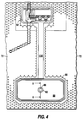
- Figure 4 is an enlarged top view of a portion of the power MOSFET shown in Figure 3.
- Figure 5 is a further enlarged top view of a portion of the power MOSFET shown in Figure 4.
- Figure 6 is a sectional view taken along line 6-6 of Figure 5.
- Figure 7 is a sectional view taken along line 7-7 of Figure 5.
- Figure 8 is a sectional view taken along line 8-8 of Figure 4.
- Figure 9 is a schematic circuit diagram of the MOSFET of the present invention.
- the power MOSFET 42 of the present invention is similar to the VDMOS 10 shown in Figure 1 in that it comprises a substrate 44 of a semiconductor material, such as silicon, having opposed first and second surfaces 46 and 48. Disposed across the second surface 48 is a relatively high conductivity region 50 of one conductivity type, shown as N+ type, which is referred to as the drain region. Contiguous with the drain region 50 and extending to the first surface 46 is a low conductivity region 52 of the one conductivity type, shown as N- type, which is referred to as the extended drain region.
- Extending into the substrate 44 from the first surface 46 are a plurality of spaced low conductivity body regions 54 of the opposite conductivity type, shown as P- type. Each of the body regions 54 forms a body/drain PN junction 56 with the extended drain region 52, the intercept of which with the first surface 46 is in the form of a hexagon. The body regions 54 are arranged along the first surface 46 in an array of rows and columns. Extending into the substrate 44 from the first surface 46 within the boundary of each of the body regions 54 is a high conductivity source region 58 of the one conductivity type, shown as N+ type which forms a source/body PN junction 60 with its respective body region 54. Each source region 58 and its associated body region 54 is commonly referred to as a source/body cell.
- each source/body PN junction 60 is spaced from a respective body/drain PN junction 56 at the first surface 46 to define the length and width of a channel region 62 in the body region 54 at the first surface 46.
- the source regions 58 are annular in shape and the outer portions of the source/body PN junctions 60 intercept the first surface 46 in the form of hexagons which are concentric with the corresponding body/drain PN junction 56 intercepts.
- each body region 54 Extending from the first surface 46 into the central portion of each body region 54, and surrounded by the annular source region 58, is a highly conductive supplementary body region 64 of the opposite conductivity type, shown as P+ type.
- the supplementary body region 64 extends to a depth which is typically greater than that of the body regions 54.
- an insulated gate electrode Disposed on the first surface 46 and over the channel regions 62 is an insulated gate electrode which comprises gate insulation 66 on the first surface 46 and a gate electrode 68 on the gate insulation 66.
- the gate insulation 66 is typically comprised of silicon dioxide in the thickness range of approximately 50 to 200 nm (500 to 2,000 angstroms) and the gate electrode 68 typically comprises doped polycrystalline silicon.
- An insulating layer 70 typically comprising a silicate glass, such as phosphosilicate glass (PSG), borosilicate glass (BSG) or borophosphosilicate glass (BPSG), overlies the gate electrode 68 so as to electrically isolate the electrode from overlying layers.
- PSG phosphosilicate glass
- BSG borosilicate glass
- BPSG borophosphosilicate glass
- a first source electrode 72 overlies the insulating layer 70 and contacts the source regions 58 and supplementary body regions 64 of a first portion of the source/body cells.
- a second source electrode 74 overlies the insulating layer 70 and contacts the source regions 58 and supplementary body regions 64 of a second portion of the source/body cells.
- the number of source/body cells contained in the second portion is much smaller than the number of source/body cells in the first portion. Typically, the number of source/body cells in the second portion contacted by the second source electrode 74 is about 1/250 of the total number of source/body cells in the substrate 44.
- the second portion of the source/body cells will be referred to as the "pilot" portion.
- the first source electrode 72 extends to a source contact pad 76 which overlies a portion of the first surface 46 which typically does not contain any source/body cells.
- a drain electrode 78 is on the second surface 48 and contacts the drain region 50.
- a first well 80 of the opposite conductivity type extends into the substrate 44 from the first surface 46 in an area of the first surface 46 which does not contain any source/body cells.
- a region 82 of the one conductivity type extends into the substrate 44 from the first surface 46 within the first well 80 and forms a PN junction 84 with the well 80. Region 82 is designed to form a zener diode D1 in the well 80.
- a gate bond pad 88 typically of a metal, extends over the area of the first surface 44 which does not contain source/body cells and which contains the first well 80 and is insulated therefrom by the insulating layer 70. The gate bond pad 88 extends through an opening 86 in the insulating layer 70 to contact region 82 of the zener diode D1.
- a second well 92 of the opposite conductivity type extends into the substrate 44 from the first surface 46 in another area of the first surface 46 which does not contain source/body cells and which is spaced from the area of the first surface 46 which contains the zener diode D1.
- a plurality of small regions 94 of the one conductivity type shown as N-type, extend into the substrate 44 from the first surface 46 within the second well 92.
- a larger region 96 of the one conductivity type, shown as N-type extends into the substrate 44 from the first surface 46 within the second well 92 and surrounds the small regions 94.
- the well 92 and the regions 94 and 96 form a lateral bipolar transistor Q1 in which the small regions 94 are the emitters, the larger region 96 is the collector and the well 92 is the base.
- the insulating layer 70 extends over the second well 92.
- First source electrode 72 extends through openings 100 in the insulating layer 70 to contact the emitter region 94, and collector contacts 102 extend through openings 104 in the insulating layer 70 to contact the collector region 96.
- the second source electrode 74 extends across the second well 92 and through openings 108 in the insulating layer 70 to contact the resistor strips 106 at one end thereof.
- the second source electrode 74 also extends through an opening 110 in the insulating layer 70 to contact the second well 92 and thereby connect the second source electrode 74 to the base of the bipolar transistor Q1.
- the first source electrode 72 extends over the second well 92 and through openings 112 in the insulating layer 70 to contact the resistor strips 106 spaced from the ends thereof.
- the first source electrode 72 also makes contact to the emitter contacts 98 of the bipolar transistor Q1.
- a strip 114 of doped polycrystalline silicon extends over and is insulated from the first surface 46 across an area of the first surface 46 which does not contain any source/body cells between the first well 80 and the second well 92.
- the strip 114 forms a resistor Rg.
- One end of the resistor strip 114 is connected to the portion of the gate bond pad 88 over the first well 80 so as to be connected to one side of the zener diode D1.
- a connection 116 extends to and makes contact with the gate electrode 68 so that the other end of the resistor Rg is connected to the gate of the power transistor Q2.
- the connection 116 also makes contact with the collector contacts 102 so that the resistor Rg is also connected to the collector of the bipolar transistor Q1.
- the above structure provides a power MOSFET having a current limiting circuit therein as shown in Figure 9.
- the zener diode D1 formed by the N-type region 82 in the first well 80 has one side connected to the gate pad 88 and the other side connected to first source electrode 72 through first well 80.
- One end of the resistor Rg formed by the strip 114 is connected to gate bond pad 88 and the other end of the resistor Rg is connected by the connection 116 to the gate electrode 68 of the power MOSFET Q2 and to the collector 96 of the bipolar transistor Q1 through the collector contacts 102.
- the base of the bipolar transistor Q1 formed by the second well 92 is connected to the source regions 58 of the pilot portion of the source/body cells through the second source electrode 74.
- the base of the bipolar transistor Q1 and the source regions 58 of the pilot portion of the source/body cells are also connected by the second source electrode 74 to one end of the resistor strips 106 forming resistor Rp.
- the other end of the resistor Rp is connected by the first source electrode 72 to the source regions 58 of the first portion of the source/body cells and to the source electrode pad 76.
- the source regions 58 of the first portion of the source/body cells are also connected by the first source electrode 72 to the emitters 94 of the bipolar transistor Q1 through the emitter contacts 98 and to the other side of the zener diode D1.
- the diodes D2 and D3 are the parasitics formed in the power MOSFET structure and provide the avalanche voltage value for the device.
- the current limiting circuit is connected across the gate of the power MOSFET Q2 and the source regions of the pilot portion of the source/body cells.
- the current limiting circuit operates in the same manner as described above for the current limiting circuit shown in Figure 2.
- the circuit is connected across the pilot portion of the source/body cells, which contains much fewer cells than the total number of cells in the MOSFET, the current flowing within the resistor Rp to turn on the bipolar transistor Q1 is much smaller.
- the power dissipation within the resistor Rp is much smaller.
- the power dissipation within the resistor Rp is reduced by a factor of 250.
- the power MOSFET 42 has the various components of the current limiting circuit incorporated therein, it can still be made using the steps of a standard method for making power MOSFET's.
- the P-type conductivity first and second wells 80 and 92 are formed at the same time as the P-type conductivity body regions 54.
- the N-type region 82 of the zener diode D1 and the N-type emitter and collector regions 94 and 96 of the bipolar transistor Q1 are formed at the same time as the N-type conductivity source regions 58.
- the strips 106 forming the resistor Rp and the strip 114 forming the resistor Rg are formed from the same doped polycrystalline silicon layer which forms the gate electrode 68.
- the second source electrode 74 is formed from the same layer of conductive material which forms the first source electrode 72.
- a power MOSFET having a current limiting circuit formed in the same substrate containing the power MOSFET.
- the current limiting circuit is connected between a pilot portion of the source regions of the MOSFET and the gate electrode so that the power dissipated within the current limiting circuit is greatly reduced over the prior art circuit.
- the current limiting circuit can be formed in the power MOSFET using the same steps as normally used to form a power MOSFET so that the cost of forming the MOSFET with the current limiting circuit is not substantially increased over that of forming a power MOSFET alone.
Landscapes
- Metal-Oxide And Bipolar Metal-Oxide Semiconductor Integrated Circuits (AREA)
- Hardware Redundancy (AREA)
- Computer And Data Communications (AREA)
- Insulated Gate Type Field-Effect Transistor (AREA)
Abstract
Claims (5)
- Transistor de puissance MOS comprenant :un substrat (44) de matériau semiconducteur de conductibilité de type un ayant des première et deuxième surfaces opposées (46, 48) ;une zone du drain (50) s'étendant à travers ledit substrat (44) entre lesdites surfaces ;une pluralité de zones du corps espacées (54) du type de conductibilité opposé dans ledit substrat (44) au niveau de ladite surface (46), chacune desdites zones du corps (54) formant une jonction corps/drain (56) avec la zone du drain ;une zone de la source séparée (58) du premier type de conductibilité dans ledit substrat (44) au niveau de la première surface (46) et à l'intérieur de chaque zone du corps (54), chacune desdites zones de la source (58) formant une jonction source/corps (60) avec ses zones du corps respectives qui est espacée de la jonction corps/drain (56) de sa zone du corps respectif pour former une zone du canal (62) entre les deux le long de la première surface (46), chacune des zones de la source (58) et leurs zones du corps respectives (54) formant une cellule source/corps ;une grille conductrice (68) placée au-dessus et isolée de ladite première surface (46) et s'étendant à travers les zones du canal (62) ;une première électrode conductrice (72) placée au-dessus et isolée de ladite grille (68) et établissant un contact avec une première partie des cellules source/corps ;une deuxième électrode conductrice (74) placée au-dessus et isolée de ladite grille (68) et établissant un contact avec une deuxième partie des cellules source/corps, le nombre de cellules source/corps contenues dans la deuxième partie étant inférieur au nombre de celles contenues dans la première partie ;un transistor bipolaire (Q1) dans ledit substrat au niveau de ladite première surface ayant une zone formant collecteur, une zone formant émetteur et une zone formant base ; caractérisé par :une diode Zener (D1) dans le substrat au niveau de ladite première surface, ladite diode ayant des première et deuxième zones du type de conductibilité opposé, dans lesquelles la diode (D1) comprend une première zone formant puits (80) du type de conductibilité opposé dans le substrat (44) au niveau de ladite première surface (46), et une zone (82) du premier type de conductibilité au niveau de ladite première surface (46) à l'intérieur de ladite zone formant puits (80) ; etdes première et deuxième résistances (Rg, Rp) placées au-dessus et isolées de ladite première surface, chacune des résistances (Rg, Rp) comprenant une bande (106, 114) de matériau partiellement conducteur placée au-dessus et isolée de ladite première surface (46), dans lesquels la bande (106) formant la deuxième résistance (Rp) se trouve au-dessus d'une deuxième zone formant puits (92) du type de conductibilité opposé contenant le transistor bipolaire (Q1) ;une extrémité de la première résistance (Rg) étant connectée à un côté de la diode (D1) et l'autre extrémité de la première résistance (Rg) étant connectée au collecteur du transistor bipolaire (Q1) et à la grille (68) ;une extrémité de la deuxième résistance (Rp) étant connectée à la base du transistor bipolaire (Q1) et à la deuxième électrode (74) ; etl'émetteur du transistor bipolaire (Q1) étant connecté à l'autre côté de la diode (D1) et à la première électrode (72).
- Transistor de puissance MOS selon la revendication 1, caractérisé en ce que le transistor bipolaire (Q1) comprend ladite deuxième zone formant puits (92) du type de conductibilité opposé dans le substrat (44) au niveau de la première surface (46) servant de base, au moins une zone (96) du premier type de conductibilité dans le substrat (44) au niveau de la première surface (46) à l'intérieur de la zone formant puits (92) servant de collecteur, et au moins une zone (94) du premier type de conductibilité dans le substrat (44) au niveau de ladite surface (46) à l'intérieur de la zone formant puits (92) servant d'émetteur.
- Transistor de puissance MOS selon la revendication 2, caractérisé en ce que le transistor bipolaire (Q1) comporte une pluralité de zones formant émetteur (94) espacée de la zone formant base (92), et une zone séparée formant collecteur (96) entourant chacune des zones formant émetteur.
- Transistor de puissance MOS selon l'une des revendications 1 à 3, caractérisé en ce que la deuxième résistance (Rp) comprend une pluralité de bandes parallèles espacées (106) de matériau partiellement conducteur.
- Transistor de puissance MOS selon l'une des revendications 1 à 4, caractérisé en ce que la bande (114) formant la première résistance (Rg) s'étend entre les deux zones formant puits (80, 92).
Applications Claiming Priority (3)
| Application Number | Priority Date | Filing Date | Title |
|---|---|---|---|
| US07/447,330 US5023692A (en) | 1989-12-07 | 1989-12-07 | Power MOSFET transistor circuit |
| PCT/US1990/006797 WO1991009424A1 (fr) | 1989-12-07 | 1990-11-20 | Circuit a transistor mosfet de puissance |
| US447330 | 1995-05-22 |
Publications (3)
| Publication Number | Publication Date |
|---|---|
| EP0457886A1 EP0457886A1 (fr) | 1991-11-27 |
| EP0457886A4 EP0457886A4 (en) | 1992-06-10 |
| EP0457886B1 true EP0457886B1 (fr) | 1997-02-05 |
Family
ID=23775932
Family Applications (1)
| Application Number | Title | Priority Date | Filing Date |
|---|---|---|---|
| EP91901146A Expired - Lifetime EP0457886B1 (fr) | 1989-12-07 | 1990-11-20 | Circuit a transistor mosfet de puissance |
Country Status (5)
| Country | Link |
|---|---|
| US (1) | US5023692A (fr) |
| EP (1) | EP0457886B1 (fr) |
| JP (1) | JP3041043B2 (fr) |
| DE (1) | DE69029907T2 (fr) |
| WO (1) | WO1991009424A1 (fr) |
Families Citing this family (25)
| Publication number | Priority date | Publication date | Assignee | Title |
|---|---|---|---|---|
| US5079608A (en) * | 1990-11-06 | 1992-01-07 | Harris Corporation | Power MOSFET transistor circuit with active clamp |
| DE4120394A1 (de) * | 1991-06-20 | 1992-12-24 | Bosch Gmbh Robert | Monolithisch integrierte schaltungsanordnung |
| GB9115699D0 (en) * | 1991-07-19 | 1991-09-04 | Philips Electronic Associated | An overvoltage protected semiconductor switch |
| EP0523800B1 (fr) * | 1991-07-19 | 1998-04-08 | Philips Electronics Uk Limited | Commutateur semi-conducteur protégé contre les surtensions |
| GB9215654D0 (en) * | 1992-07-23 | 1992-09-09 | Philips Electronics Uk Ltd | A semiconductor component |
| US5408141A (en) * | 1993-01-04 | 1995-04-18 | Texas Instruments Incorporated | Sensed current driving device |
| JPH07146722A (ja) * | 1993-10-01 | 1995-06-06 | Fuji Electric Co Ltd | トランジスタ用過電流保護装置 |
| JP3018816B2 (ja) * | 1993-02-22 | 2000-03-13 | 株式会社日立製作所 | 半導体素子の保護回路ならびにこれを有する半導体装置 |
| JP2917729B2 (ja) * | 1993-03-03 | 1999-07-12 | 住友電気工業株式会社 | 光ファイバ母材の製造方法 |
| EP0625797B1 (fr) * | 1993-05-19 | 1999-08-11 | Consorzio per la Ricerca sulla Microelettronica nel Mezzogiorno | Structure intégrée d'une résistance de détection de courant pour les dispositifs MOS à puissance, en particulier pour les dispositifs MOS à puissance autoprotégés contre la surcharge |
| US5691555A (en) * | 1993-05-19 | 1997-11-25 | Consorzio Per La Ricerca Sulla Microelettronica Nel Mezzogiorno | Integrated structure current sensing resistor for power devices particularly for overload self-protected power MOS devices |
| US5373434A (en) * | 1994-03-21 | 1994-12-13 | International Business Machines Corporation | Pulse width modulated power supply |
| DE59409484D1 (de) * | 1994-10-28 | 2000-09-21 | Siemens Ag | Festkörperschaltelement mit zwei source-elektroden und festkörperschalter mit einem solchen element |
| US5665996A (en) * | 1994-12-30 | 1997-09-09 | Siliconix Incorporated | Vertical power mosfet having thick metal layer to reduce distributed resistance |
| US5767546A (en) * | 1994-12-30 | 1998-06-16 | Siliconix Incorporated | Laternal power mosfet having metal strap layer to reduce distributed resistance |
| US5811857A (en) * | 1996-10-22 | 1998-09-22 | International Business Machines Corporation | Silicon-on-insulator body-coupled gated diode for electrostatic discharge (ESD) and analog applications |
| US6323522B1 (en) | 1999-01-08 | 2001-11-27 | International Business Machines Corporation | Silicon on insulator thick oxide structure and process of manufacture |
| US6784486B2 (en) * | 2000-06-23 | 2004-08-31 | Silicon Semiconductor Corporation | Vertical power devices having retrograded-doped transition regions therein |
| US6781194B2 (en) * | 2001-04-11 | 2004-08-24 | Silicon Semiconductor Corporation | Vertical power devices having retrograded-doped transition regions and insulated trench-based electrodes therein |
| US6392463B1 (en) * | 2000-07-07 | 2002-05-21 | Denso Corporation | Electrical load driving circuit with protection |
| JP4198469B2 (ja) * | 2001-04-11 | 2008-12-17 | シリコン・セミコンダクター・コーポレイション | パワーデバイスとその製造方法 |
| US7139157B2 (en) * | 2004-07-30 | 2006-11-21 | Kyocera Wireless Corp. | System and method for protecting a load from a voltage source |
| US8345391B2 (en) * | 2009-09-17 | 2013-01-01 | Linear Technology Corporation | DC/DC converter overcurrent protection |
| GB2479535A (en) * | 2010-04-13 | 2011-10-19 | Rolls Royce Plc | Current limiter for a vehicle power distribution network |
| DE112022000785T5 (de) | 2021-03-22 | 2023-11-16 | Rohm Co., Ltd. | Schaltvorrichtung, elektronisches gerät und fahrzeug |
Citations (1)
| Publication number | Priority date | Publication date | Assignee | Title |
|---|---|---|---|---|
| DE3821065A1 (de) * | 1987-06-22 | 1989-01-05 | Nissan Motor | Mos-feldeffekttransistor-einrichtung |
Family Cites Families (5)
| Publication number | Priority date | Publication date | Assignee | Title |
|---|---|---|---|---|
| US4377945A (en) * | 1978-10-30 | 1983-03-29 | Giovanni Bernard A Di | Service line interior by-pass |
| JPS5912451Y2 (ja) * | 1979-09-11 | 1984-04-14 | トヨタ自動車株式会社 | 油圧シリンダ |
| JPS60188691A (ja) * | 1984-03-08 | 1985-09-26 | 積水プラントシステム株式会社 | 地下埋没管の補修方法 |
| US4631564A (en) * | 1984-10-23 | 1986-12-23 | Rca Corporation | Gate shield structure for power MOS device |
| US4860080A (en) * | 1987-03-31 | 1989-08-22 | General Electric Company | Isolation for transistor devices having a pilot structure |
-
1989
- 1989-12-07 US US07/447,330 patent/US5023692A/en not_active Expired - Lifetime
-
1990
- 1990-11-20 JP JP3501504A patent/JP3041043B2/ja not_active Expired - Fee Related
- 1990-11-20 DE DE69029907T patent/DE69029907T2/de not_active Expired - Fee Related
- 1990-11-20 WO PCT/US1990/006797 patent/WO1991009424A1/fr not_active Ceased
- 1990-11-20 EP EP91901146A patent/EP0457886B1/fr not_active Expired - Lifetime
Patent Citations (1)
| Publication number | Priority date | Publication date | Assignee | Title |
|---|---|---|---|---|
| DE3821065A1 (de) * | 1987-06-22 | 1989-01-05 | Nissan Motor | Mos-feldeffekttransistor-einrichtung |
Also Published As
| Publication number | Publication date |
|---|---|
| DE69029907T2 (de) | 1997-09-04 |
| US5023692A (en) | 1991-06-11 |
| DE69029907D1 (de) | 1997-03-20 |
| EP0457886A4 (en) | 1992-06-10 |
| EP0457886A1 (fr) | 1991-11-27 |
| JP3041043B2 (ja) | 2000-05-15 |
| WO1991009424A1 (fr) | 1991-06-27 |
| JPH05503190A (ja) | 1993-05-27 |
Similar Documents
| Publication | Publication Date | Title |
|---|---|---|
| EP0457886B1 (fr) | Circuit a transistor mosfet de puissance | |
| US5652689A (en) | ESD protection circuit located under protected bonding pad | |
| US5548134A (en) | Device for the protection of an integrated circuit against electrostatic discharges | |
| US5717559A (en) | Input/output protection device for use in semiconductor device | |
| US6236087B1 (en) | SCR cell for electrical overstress protection of electronic circuits | |
| US4139935A (en) | Over voltage protective device and circuits for insulated gate transistors | |
| US5432368A (en) | Pad protection diode structure | |
| US4819044A (en) | Vertical type MOS transistor and its chip | |
| US4686551A (en) | MOS transistor | |
| JPS6358380B2 (fr) | ||
| JPS6153761A (ja) | 半導体装置 | |
| US4806999A (en) | Area efficient input protection | |
| EP0242383B1 (fr) | Protection de circuits integres igfet contre les decharges electrostatiques | |
| EP0768713A2 (fr) | Circuit comprenant des moyens de protection | |
| EP0472654B1 (fr) | Dispositif de retour a zero declenche par de faibles tensions | |
| US5798538A (en) | IGBT with integrated control | |
| US4599631A (en) | Semiconductor apparatus having a zener diode integral with a resistor-transistor combination | |
| EP0494184B1 (fr) | Dispositif mos comprenant une protection integree contre la decharge electrostatique | |
| US5109266A (en) | Semiconductor integrated circuit device having high breakdown-voltage to applied voltage | |
| US6127723A (en) | Integrated device in an emitter-switching configuration | |
| US5068703A (en) | Electronic circuit device | |
| KR100206675B1 (ko) | 반도체 집적 회로 장치 | |
| US6320229B1 (en) | Semiconductor device | |
| JPH05505060A (ja) | 低トリガ電圧scr保護装置及び構造 | |
| EP1190450B1 (fr) | Protection de circuits integres contre la decharge electrostatique |
Legal Events
| Date | Code | Title | Description |
|---|---|---|---|
| PUAI | Public reference made under article 153(3) epc to a published international application that has entered the european phase |
Free format text: ORIGINAL CODE: 0009012 |
|
| 17P | Request for examination filed |
Effective date: 19910725 |
|
| AK | Designated contracting states |
Kind code of ref document: A1 Designated state(s): DE ES FR GB IT NL |
|
| A4 | Supplementary search report drawn up and despatched |
Effective date: 19920423 |
|
| AK | Designated contracting states |
Kind code of ref document: A4 Designated state(s): DE ES FR GB IT NL |
|
| 17Q | First examination report despatched |
Effective date: 19940412 |
|
| GRAG | Despatch of communication of intention to grant |
Free format text: ORIGINAL CODE: EPIDOS AGRA |
|
| GRAH | Despatch of communication of intention to grant a patent |
Free format text: ORIGINAL CODE: EPIDOS IGRA |
|
| GRAH | Despatch of communication of intention to grant a patent |
Free format text: ORIGINAL CODE: EPIDOS IGRA |
|
| GRAA | (expected) grant |
Free format text: ORIGINAL CODE: 0009210 |
|
| AK | Designated contracting states |
Kind code of ref document: B1 Designated state(s): DE ES FR GB IT NL |
|
| PG25 | Lapsed in a contracting state [announced via postgrant information from national office to epo] |
Ref country code: NL Free format text: LAPSE BECAUSE OF FAILURE TO SUBMIT A TRANSLATION OF THE DESCRIPTION OR TO PAY THE FEE WITHIN THE PRESCRIBED TIME-LIMIT Effective date: 19970205 Ref country code: ES Free format text: THE PATENT HAS BEEN ANNULLED BY A DECISION OF A NATIONAL AUTHORITY Effective date: 19970205 |
|
| ET | Fr: translation filed | ||
| REF | Corresponds to: |
Ref document number: 69029907 Country of ref document: DE Date of ref document: 19970320 |
|
| ITF | It: translation for a ep patent filed | ||
| NLV1 | Nl: lapsed or annulled due to failure to fulfill the requirements of art. 29p and 29m of the patents act | ||
| PLBE | No opposition filed within time limit |
Free format text: ORIGINAL CODE: 0009261 |
|
| STAA | Information on the status of an ep patent application or granted ep patent |
Free format text: STATUS: NO OPPOSITION FILED WITHIN TIME LIMIT |
|
| 26N | No opposition filed | ||
| PGFP | Annual fee paid to national office [announced via postgrant information from national office to epo] |
Ref country code: GB Payment date: 20011107 Year of fee payment: 12 |
|
| REG | Reference to a national code |
Ref country code: GB Ref legal event code: IF02 |
|
| PG25 | Lapsed in a contracting state [announced via postgrant information from national office to epo] |
Ref country code: GB Free format text: LAPSE BECAUSE OF NON-PAYMENT OF DUE FEES Effective date: 20021120 |
|
| GBPC | Gb: european patent ceased through non-payment of renewal fee | ||
| PG25 | Lapsed in a contracting state [announced via postgrant information from national office to epo] |
Ref country code: IT Free format text: LAPSE BECAUSE OF NON-PAYMENT OF DUE FEES;WARNING: LAPSES OF ITALIAN PATENTS WITH EFFECTIVE DATE BEFORE 2007 MAY HAVE OCCURRED AT ANY TIME BEFORE 2007. THE CORRECT EFFECTIVE DATE MAY BE DIFFERENT FROM THE ONE RECORDED. Effective date: 20051120 |
|
| PGFP | Annual fee paid to national office [announced via postgrant information from national office to epo] |
Ref country code: FR Payment date: 20071119 Year of fee payment: 18 |
|
| PGFP | Annual fee paid to national office [announced via postgrant information from national office to epo] |
Ref country code: DE Payment date: 20071221 Year of fee payment: 18 |
|
| REG | Reference to a national code |
Ref country code: FR Ref legal event code: ST Effective date: 20090731 |
|
| PG25 | Lapsed in a contracting state [announced via postgrant information from national office to epo] |
Ref country code: DE Free format text: LAPSE BECAUSE OF NON-PAYMENT OF DUE FEES Effective date: 20090603 |
|
| PG25 | Lapsed in a contracting state [announced via postgrant information from national office to epo] |
Ref country code: FR Free format text: LAPSE BECAUSE OF NON-PAYMENT OF DUE FEES Effective date: 20081130 |