EP0458055A2 - Pulse width modulation method for a convertor - Google Patents
Pulse width modulation method for a convertor Download PDFInfo
- Publication number
- EP0458055A2 EP0458055A2 EP19910105924 EP91105924A EP0458055A2 EP 0458055 A2 EP0458055 A2 EP 0458055A2 EP 19910105924 EP19910105924 EP 19910105924 EP 91105924 A EP91105924 A EP 91105924A EP 0458055 A2 EP0458055 A2 EP 0458055A2
- Authority
- EP
- European Patent Office
- Prior art keywords
- switching
- power transistors
- pulse
- voltage
- signal
- Prior art date
- Legal status (The legal status is an assumption and is not a legal conclusion. Google has not performed a legal analysis and makes no representation as to the accuracy of the status listed.)
- Withdrawn
Links
Images


Classifications
-
- H—ELECTRICITY
- H02—GENERATION; CONVERSION OR DISTRIBUTION OF ELECTRIC POWER
- H02M—APPARATUS FOR CONVERSION BETWEEN AC AND AC, BETWEEN AC AND DC, OR BETWEEN DC AND DC, AND FOR USE WITH MAINS OR SIMILAR POWER SUPPLY SYSTEMS; CONVERSION OF DC OR AC INPUT POWER INTO SURGE OUTPUT POWER; CONTROL OR REGULATION THEREOF
- H02M7/00—Conversion of AC power input into DC power output; Conversion of DC power input into AC power output
- H02M7/42—Conversion of DC power input into AC power output without possibility of reversal
- H02M7/44—Conversion of DC power input into AC power output without possibility of reversal by static converters
- H02M7/48—Conversion of DC power input into AC power output without possibility of reversal by static converters using discharge tubes with control electrode or semiconductor devices with control electrode
- H02M7/53—Conversion of DC power input into AC power output without possibility of reversal by static converters using discharge tubes with control electrode or semiconductor devices with control electrode using devices of a triode or transistor type requiring continuous application of a control signal
- H02M7/537—Conversion of DC power input into AC power output without possibility of reversal by static converters using discharge tubes with control electrode or semiconductor devices with control electrode using devices of a triode or transistor type requiring continuous application of a control signal using semiconductor devices only, e.g. single switched pulse inverters
- H02M7/539—Conversion of DC power input into AC power output without possibility of reversal by static converters using discharge tubes with control electrode or semiconductor devices with control electrode using devices of a triode or transistor type requiring continuous application of a control signal using semiconductor devices only, e.g. single switched pulse inverters with automatic control of output wave form or frequency
- H02M7/5395—Conversion of DC power input into AC power output without possibility of reversal by static converters using discharge tubes with control electrode or semiconductor devices with control electrode using devices of a triode or transistor type requiring continuous application of a control signal using semiconductor devices only, e.g. single switched pulse inverters with automatic control of output wave form or frequency by pulse-width modulation
-
- H—ELECTRICITY
- H02—GENERATION; CONVERSION OR DISTRIBUTION OF ELECTRIC POWER
- H02M—APPARATUS FOR CONVERSION BETWEEN AC AND AC, BETWEEN AC AND DC, OR BETWEEN DC AND DC, AND FOR USE WITH MAINS OR SIMILAR POWER SUPPLY SYSTEMS; CONVERSION OF DC OR AC INPUT POWER INTO SURGE OUTPUT POWER; CONTROL OR REGULATION THEREOF
- H02M7/00—Conversion of AC power input into DC power output; Conversion of DC power input into AC power output
- H02M7/42—Conversion of DC power input into AC power output without possibility of reversal
- H02M7/44—Conversion of DC power input into AC power output without possibility of reversal by static converters
- H02M7/48—Conversion of DC power input into AC power output without possibility of reversal by static converters using discharge tubes with control electrode or semiconductor devices with control electrode
- H02M7/53—Conversion of DC power input into AC power output without possibility of reversal by static converters using discharge tubes with control electrode or semiconductor devices with control electrode using devices of a triode or transistor type requiring continuous application of a control signal
- H02M7/537—Conversion of DC power input into AC power output without possibility of reversal by static converters using discharge tubes with control electrode or semiconductor devices with control electrode using devices of a triode or transistor type requiring continuous application of a control signal using semiconductor devices only, e.g. single switched pulse inverters
- H02M7/538—Conversion of DC power input into AC power output without possibility of reversal by static converters using discharge tubes with control electrode or semiconductor devices with control electrode using devices of a triode or transistor type requiring continuous application of a control signal using semiconductor devices only, e.g. single switched pulse inverters in a push-pull configuration
-
- H—ELECTRICITY
- H03—ELECTRONIC CIRCUITRY
- H03K—PULSE TECHNIQUE
- H03K17/00—Electronic switching or gating, i.e. not by contact-making and –breaking
- H03K17/14—Modifications for compensating variations of physical values, e.g. of temperature
-
- H—ELECTRICITY
- H03—ELECTRONIC CIRCUITRY
- H03K—PULSE TECHNIQUE
- H03K17/00—Electronic switching or gating, i.e. not by contact-making and –breaking
- H03K17/51—Electronic switching or gating, i.e. not by contact-making and –breaking characterised by the components used
- H03K17/56—Electronic switching or gating, i.e. not by contact-making and –breaking characterised by the components used by the use, as active elements, of semiconductor devices
- H03K17/60—Electronic switching or gating, i.e. not by contact-making and –breaking characterised by the components used by the use, as active elements, of semiconductor devices the devices being bipolar transistors
- H03K17/66—Switching arrangements for passing the current in either direction at will; Switching arrangements for reversing the current at will
Definitions
- the invention relates to a method according to the preamble of patent claim 1.
- converter output currents can be generated with a high degree of efficiency in accordance with a strongly variable setpoint. Due to the storage time when the switching transistors are switched off, there are longer switch-on signals at the converter output. This leads to problems that have to be taken into account when controlling or generating the pulse-width-modulated switching signals. It is particularly important to ensure that the switching transistor in the other bridge branch is not switched on during the extended switch-on time and that a short-circuit current which is too great is thereby generated. To avoid this it is known, e.g. B.
- EP-PS 01 24 619 via timers to provide a lock that blocks the switching on of the other switching transistor for a predetermined time after the completion of each switch-on pulse.
- this locking takes place via AND gates through a hysteresis circuit with the aid of RC elements. Since the storage time of the switching transistors depends on the temperature, the voltage and the current, and above all increases disproportionately with large load currents and high chip temperature, the two switching transistors must be one Half-bridge can be locked against each other by means of a dead time that corresponds to the maximum possible storage time plus a safety time.
- the object is achieved to adapt the dead time of the switching transistors to the actual switching and / or storage time, as it arises in the current operating state.
- a switching voltage is generated from the base-emitter voltage of the switching transistors, and this is used to lock the other switching transistor of the bridge branch during the storage time currently in progress.
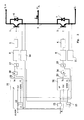
- Fig. 1 two high-voltage power transistors 1 and 2 of a bridge arm are switched from driver stages 3 and 4 in the blocked or saturated region.
- the collector of the power transistor 1 is connected to the positive pole of the supply voltage L + of the power section
- the emitter is connected to the collector of the power transistor 2 of the other bridge branch, the emitter of which is connected to the negative pole L- of the supply voltage.
- U A At the emitter-collector connection 5 between the two transistors 1 and 2 there is the output voltage U A , which is led to a load.
- This bridge branch switched in a known manner can be part of a bridge circuit which, for. B. is in triplicate at the positive and negative output of a DC link and their respective emitter-collector connections 5 is at a winding end of a three-phase winding for a servo motor.
- the control of the power transistors 1 and 2 via the driver stages 3 and 4 and the construction of these driver stages can be carried out in the same way as is shown in DE-OS 35 22 429.
- the switching signals are fed to driver stages 3 and 4 in the same way via electrical isolation stages 8 and 9.
- the base-emitter voltage is tapped at each of the two power transistors 1 and 2 and each is fed to the input of a step trigger 12 and 13 via a further potential isolating stage 10 and 11.
- the output of the step trigger 12 for the base-emitter voltage of the power transistor 1 connected to the positive supply voltage L + is connected to the R input of a D flip-flop 14 and to the first input of an OR gate 15.
- the pulse-width-modulated control signal X is applied, which is fed via a negator 16 and a further OR gate 17 to the negated input of the potential isolation stage 8 and further via a further OR gate 18 with the Input of the potential isolation stage 9 is connected.
- the control signal X can be generated in a known manner in a microprocessor and / or counter stages or by voltage comparison with a delta voltage. If it assumes a high level, a low level is applied via the negator 16 to the input of the potential isolation stage 8, which, for. B. via a light-emitting diode of an optocoupler with its other end at the positive pole of a supply voltage (not shown), a signal to the input of driver stage 3 given that the power transistor 1 controls in the saturation range.
- the base of the power transistor assumes a voltage which is positive with respect to the emitter and which sets the output of the Schmitt trigger 12 to a high level via the potential isolating stage 10.
- control signal X switches to a low level, a high level reaches the input of the potential isolation stage 8 via the negator 16, as a result of which the power transistor 1 is opened or switched to a high-resistance state via the driver stage 3.
- switching to this state does not take place immediately, but in a known manner only after a storage time has elapsed, the time period of which depends on the temperature in the power transistor, the voltages applied to it and the currents flowing through it. This storage time increases disproportionately, especially with large currents. As long as a current flows through the power transistor 1, that is to say also during the storage time, a voltage drop occurs at the base-emitter path, which drops to a high level at the output of the Schmitt trigger 12.
- the control signal at the D input is retained until after the storage time at the Q output of the D flip-flop.
- the time of the output signal UA * applied to this Q output therefore largely corresponds to the time of the output voltage U A applied to the load. So that this correspondence is also given with a different current direction or changing current direction by the load, it will be necessary, as will be explained later, to make the switching of the D flip-flop 14 dependent on a clock pulse which is caused by the positive edges of the Output signals of the two Schmitt triggers 12 and 13 is effected.
- the output signals from the Schmitt triggers 12 and 13 are led to the OR gate, the output of which is connected to the clock input of the D flip-flop via a time stage 19.
- the time step delays the signal only insignificantly, but ensures that the signals are safely applied to the R and S inputs before a clock is generated.
- the power transistor 7 can be controlled to saturation, provided that no current flows through the freewheeling diode 7, which also applies to the power transistor 1 when a current flows through the diode 6, such as will be explained later.
- the output voltage UA * on the D flip-flop 14 can now be used when generating the control signal, for. B. by a corresponding intervention in the control circuit to carry out a correction, since this corresponds to the actual duty cycle of the power transistors 1 and / or 2.
- the output signal of the Schmitt triggers 12 and 13 is further fed to the second input of the OR gate 17 or 18 of the other bridge branch and ensures that a high level is present at the output of the respective OR gate 17 or 18 as long as a current flows through the power transistor 1 or 2 of the other bridge branch, the actual storage time of the power transistors 1 and 2 also being detected.
- a correction of the storage time of the power transistors 1 and 2 is provided in FIG. 2 for a power stage switched and driven in the same way (the same reference numbers are used).
- the other bridge branch is locked in the same way via the Schmitt triggers 12 and 13 and the OR gates 17 and 18.
- the control of the OR gate 17 takes place here instead of the negator 16 via a NAND gate 20, the second one Input at the output of an up / down counter 21 is.
- the control input X is fed to the UP input of this up / down counter 21 and the DOWN input is connected to the output of the Schmitt trigger 12.
- the clock pulses supplied to a clock input CLK of a higher-frequency pulse series, e.g. B. from a microprocessor, the counter being set to zero by a signal at the clear input CL can be.
- This clear input CL is connected to the output of the Schmitt trigger 13 of the other bridge branch.
- a high level is always present at the output 22 of the up / down counter 21 when the counter contains zero or positive values. If the control signal X is positive, a switching signal with a counter reading of zero reaches the driver stage 3 via the NAND gate 20 and the OR gate 17, which switches the power transistor 1 into the saturation range. A short count is made until a corresponding signal from the base-emitter voltage reaches the DOWN input of the up / down counter 21 via the Schmitt trigger 12, whereby essentially the switch-on delay time of the power transistor 1, which is considerably shorter than the switch-off storage time, is recorded. The now positive output signal at the Schmitt trigger 12 stops the counting up, or there is an up / down counting with the same clock pulses, since the DOWN input is now also activated.
- the control of the power transistor 2 takes place with the low level of the control signal X, which is connected via a negator 23 to the UP input of a further up / down counter 24, the clock input CLK of which are supplied with the same clock signals and at the latter DOWN input, the output signals of the Schmitt trigger 13 are.
- the output 25 of the up / down counter 24 constructed in the same way outputs a high level to an input of a further NAND gate 26 whenever the counter reading is zero or positive.
- the control signals inverted via the inverter 23 are delayed in the same way as the control signals for the first bridge branch. If the current at the output UA changes with the other bridge branch when the current direction changes, the up / down counter is set to zero when the other power transistor is switched through.
- FIG. 3 shows a circuit that solves both tasks according to FIG. 1 and FIG. 2. 1 (with the same reference numbers) are connected to one another in the same way, the timing element 19 in front of the clock input of the D flip-flop 14 consisting of two successive negators.
- the isolating stages 8 to 11 are provided with optocouplers, the base of the respective power transistor 1 or 2 being located at a light-emitting diode input of the isolating stages 10 and 11 for detecting the base-emitter voltage.
- the cathode of a diode 31 and 32 is connected to the emitter of the power transistors 1 and 2, and a respective resistor 33 and 34 is connected in parallel.
- the anode of the diodes 31 and 32 lies in each case on the anode of a further diode 35 and 36, the cathode of which is connected to the second light-emitting diode input of the respective isolating stage 10 and 11 is.
- the connection of the two diodes 31 with 35 and 32 with 36 is connected via a capacitor 37 and 38 to the base of the power transistor 1 and 2, respectively.
- the resistor 33 and 34 is dimensioned so that with a high-impedance switched power transistor 1 or 2 with a negative base voltage from the driver stages 3 or 4 a predetermined current through the respective light-emitting diode of the isolating stages 10 or 11, the diode 35 or 36 and the resistor 33 or 34 flows, which causes a positive supply voltage via a resistor 39 or 40 at the output of the isolating stage 10 or 11 to break down to zero.
- the counter stages 21 and 24 according to FIG. 2 are replaced here by a commercially available binary counter 42 and 43 (e.g. an integrated circuit 4520) and a programmable downward binary counter 44 and 45 (e.g. an integrated circuit 4526) , whereby during the storage time of the corresponding power transistors 1 or 2 the respective binary counter 42 or 43 counts up clock pulses, with this number the respective binary counter 44 or 45 is programmed and the switching through is delayed with the next switching pulse until the programmed value returns to zero is counted down.
- a clock pulse signal according to FIG. 2 is fed to each clock input of the four binary counters 42 to 45.
- An increment of binary counters 42 or 43 always occurs only when there is a positive signal at the output of an AND gate 48 or 49, which is also connected to the enable input of the AND gate 48 or 49, also assumes a positive value. However, this is essentially only the case during the storage time of the corresponding power transistor 1 or 2.
- the binary counter 42 or 43 With each negative switch-on pulse edge at the output of the OR gate 17 or 18, the binary counter 42 or 43 is set to zero via a clear input CL via an amplifier 50 or 51, a capacitor 52 or 53 and a negator 54 or 55. At the input of the negators 54 and 55 there is in each case the anode of a diode 56, 57 and a resistor 58, 59, which have their other end or the cathode at the positive pole of the supply voltage. This suppresses the positive edge of the switching voltage.
- a delay circuit consisting of a resistor 62 or 63 with a diode 64 or 65 connected in parallel, one at the input of the OR -Gatter lying capacitor 66 and 67 charges.
- This delay circuit causes the front positive pulse edge to reach the OR gate 17 or 18 without delay, but the rear negative pulse edge has a sufficiently positive signal present at the input of the OR gate 17 or 18 for a while. This ensures that the respective power transistor 1 or 2 remains blocked until the other power transistor 2 or 1 is completely switched into the high-resistance range.
- the power transistors 1 and 2 can consist of several power transistors interconnected in a known manner, and the load at the output U A can be a strongly inductive load, e.g. B. the phase winding of a servo motor.
- the load at the output U A can be a strongly inductive load, e.g. B. the phase winding of a servo motor.
- voltages and currents result in the circuits according to FIGS. 1 to 3, as occur in FIGS. 4 to 6 with different load currents.
- the control signal X and a positive load current I is shown.
- the load current I should increase during the time t 3 to t 1 with the positive control signal X via the power transistor 1 controlled in the saturation range. Due to the storage time of this power transistor 1, a changeover to the high-resistance region takes place only at time t 2. Without a correction of this storage time (t1 to t2), a current I * would form, which rises continuously.
- the base-emitter voltage BE1 and BE2 of the two power transistors 1 and 2 is detected and from this a switching voltage S1 and S2 present behind the Schmitt trigger 12 and 13 is obtained.
- the switch-on delay compared to the storage time usually does not play a significant role in the power transistors (the switch-on delay is, for example, 1 to 2 usec. While the storage time is 20 to 30 usec.) And the storage time is considerably longer, in particular of the load current I and the semiconductor temperature depends on the power transistors, a circuit according to FIG. 3 can be selected.
- a switching voltage Sp1 and Sp2 is generated at the output of the AND gates 48, 49, which has positive pulses that are largely present only during the storage time.
- the corresponding binary counter 42 or 43 is incremented and the corresponding programmable binary counter 44 or 45 is programmed with the incremented value.
- the next switch-on pulse is then passed on to the OR gate 17 or 18 only when the programmed value has been counted down again via the clock pulses.
- an output voltage signal UA * can also be generated from the switching signals S1 and S2, which according to FIG. 1 can be used to correct the generation of the actuating signal or according to FIG. 3 with a corrected one 4 for an additional correction, z. B. serve the curve shape for a sinusoidal total output current I in the control loop.
- Fig. 6 shows the same voltages and currents with changing load current I.
- the control signal X goes to zero and switches off the power transistor 1, the base-emitter voltage BE1 of this power transistor 1 being a negative after the storage time (t1 to t2) Assumes value.
- a current flows through the freewheeling diode 7 until the current I becomes zero.
- the power transistor 2 can turn on and the base-emitter voltage BE2 becomes positive.
- the counting up during which it is not possible to switch through during the freewheeling diode current, does not have any disadvantageous effects.
- the storage capacity does not need to be designed for this time, it is sufficient if it covers the maximum possible switch-on delay or storage time. 3 is counted up only during the duration of the storage time signals Sp1 or Sp2 at the output of the AND gate 48 or 49 and the counting out of the programmable binary counter 44 or 45 begins at the beginning of the corresponding pulse of the actuating signal X, this is done in the time in which switching is not possible due to the freewheeling diode current, so that there is no effect on the switching times of the power transistors.
Landscapes
- Engineering & Computer Science (AREA)
- Power Engineering (AREA)
- Inverter Devices (AREA)
Abstract
- 2.1 Bei der Verwendung bipolarer Leistungstransistoren ergeben sich, durch die von der Temperatur, dem Strom und der Spannung abhängige Speicherzeit der Leistungstransistoren, von den Ansteuerimpulsen abweichende Durchschaltzeiten, deren Auswirkungen vermieden werden sollen.2.1 When using bipolar power transistors, the switching times deviating from the control pulses result from the storage time of the power transistors, which is dependent on the temperature, the current and the voltage, the effects of which should be avoided.
- 2.2 Mit Hilfe der Basis-Emitter-Spannung der Leistungstransistoren lassen sich Signalspannungen erzeugen, die eine Korrektur dieser Abweichungen ermöglichen und/oder durch eine Verzögerung des folgenden Einschaltimpulses die Durchschaltzeiten an die Ansteuerimpulsbreiten anpaßt.2.2 With the aid of the base-emitter voltage of the power transistors, signal voltages can be generated which enable these deviations to be corrected and / or adapt the switching times to the drive pulse widths by delaying the subsequent switch-on pulse.
- 2.3 Hierdurch wird eine reaktionsschnelle, korrekte Regelung des Umrichterstromes möglich, die z. B. bei der Erzeugung von Wechselströmen eine bessere angepaßte Kurvenform ermöglicht.2.3 This enables a responsive, correct control of the converter current. B. allows a better adapted curve shape in the generation of alternating currents.
Description
Die Erfindung betrifft ein Verfahren gemäß dem Oberbegriff des Patentanspruches 1.The invention relates to a method according to the preamble of
Mit derartigen Verfahren lassen sich bei entsprechend hoher Frequenz der in der Impulsbreite modulierten Schaltsignale, Umrichterausgangströme entsprechend einem sich stark veränderbarem Sollwert mit hohem Wirkungsgrad erzeugen. Bedingt durch die Speicherzeit beim Ausschalten der Schalttransistoren ergeben sich hierbei am Umrichterausgang zeitlich längere Einschaltsignale. Dies führt zu Problemen, die bei der Ansteuerung bzw. Erzeugung der impulsbreitenmodulierten Schaltsignale berücksichtigt werden müssen. Besonders wichtig ist es, sicherzustellen, daß während der verlängerten Einschaltzeit kein Einschalten des Schalttransistors im anderen Brückenzweig erfolgt und hierdurch ein zu großer Kurzschlußstrom erzeugt wird. Um dies zu vermeiden ist es bekannt, z. B. gemäß der EP-PS 01 24 619 über Zeitglieder eine Verriegelung vorzusehen, die ein Einschalten des anderen Schalttransistors während einer vorgegebenen Zeit nach Beendigung jedes Einschaltimpulses sperrt. In der EP-PS 0 124 619 erfolgt diese Verriegelung über UND-Gatter durch eine Hysteresis-Schaltung mit Hilfe von RC-Gliedern. Da die Speicherzeit der Schalttransistoren von der Temperatur, der Spannung und dem Strom abhängig ist, und vor allem bei großen Lastströmen und hoher Chip-Temperatur überproportional zunimmt, müssen die beiden Schalttransistoren einer Halbbrücke mittels einer Totzeit gegeneinander verriegelt werden, die der maximal möglichen Speicherzeit zuzüglich einer Sicherheitszeit entspricht.With such methods, with a correspondingly high frequency of the switching signals modulated in the pulse width, converter output currents can be generated with a high degree of efficiency in accordance with a strongly variable setpoint. Due to the storage time when the switching transistors are switched off, there are longer switch-on signals at the converter output. This leads to problems that have to be taken into account when controlling or generating the pulse-width-modulated switching signals. It is particularly important to ensure that the switching transistor in the other bridge branch is not switched on during the extended switch-on time and that a short-circuit current which is too great is thereby generated. To avoid this it is known, e.g. B. according to EP-PS 01 24 619 via timers to provide a lock that blocks the switching on of the other switching transistor for a predetermined time after the completion of each switch-on pulse. In EP-PS 0 124 619 this locking takes place via AND gates through a hysteresis circuit with the aid of RC elements. Since the storage time of the switching transistors depends on the temperature, the voltage and the current, and above all increases disproportionately with large load currents and high chip temperature, the two switching transistors must be one Half-bridge can be locked against each other by means of a dead time that corresponds to the maximum possible storage time plus a safety time.
Ein weiteres Problem ergibt sich dadurch, daß die Einschaltdauer der Schalttransistoren nicht mit der Impulsbreite der Schaltsignale übereinstimmt, so daß eine Korrektur der Schaltsignale erfolgen muß, um korrekt dem Sollwert entsprechende Ausgangsgrößen erzielen zu können. Üblicherweise erfolgt dies innerhalb einer Regelstrecke mit linearen Reglern bzw. durch einen Soll-Istwertvergleich. Durch die nichtlineare Veränderung der Speicherzeit und dadurch, daß die Totzeit nur zeitweilig zum Tragen kommt, ist eine Korrektur mit herkömmlichen linearen Reglern nur unvollständig beherrschbar.A further problem arises from the fact that the duty cycle of the switching transistors does not match the pulse width of the switching signals, so that the switching signals must be corrected in order to be able to achieve output variables that correspond correctly to the setpoint. This is usually done within a controlled system with linear controllers or through a target / actual value comparison. Due to the non-linear change in the storage time and the fact that the dead time only comes into play temporarily, a correction with conventional linear controllers is only incompletely manageable.
So kann sich vor allem bei rasch änderndem Sollwert und insbesondere bei wechselnder Last, mit Änderungen der Stromrichtung im Lastkreis, eine störend veränderte Kurvenform der Ausgangsspannung ergeben.This can result in a disturbingly changed curve shape of the output voltage, especially with a rapidly changing setpoint and in particular with a changing load, with changes in the current direction in the load circuit.
Es ist Aufgabe der Erfindung, mit einfachen Mitteln eine Korrektur der Speicherzeit zu ermöglichen, die eine ausreichend genaue, dem Sollwert entsprechende Kurvenform der Ausgangsspannung bewirkt. Gelöst wird diese Aufgabe durch ein Verfahren und/oder eine Schaltungsanordnung mit den in den Ansprüchen gekennzeichneten Merkmalen.It is an object of the invention to enable the storage time to be corrected with simple means, which results in a sufficiently precise curve shape of the output voltage corresponding to the setpoint. This object is achieved by a method and / or a circuit arrangement with the features characterized in the claims.
In Weiterbildung der Erfindung wird die Aufgabe gelöst, die Totzeit der Schalttransistoren der eigentlichen Schalt- und/oder Speicherzeit anzupassen, wie sie in dem gerade vorliegenden Betriebszustand entsteht. Hierzu wird aus der Basis-Emitter-Spannung der Schalttransistoren eine Schaltspannung erzeugt und mit dieser eine Verriegelung des anderen Schalttransistors des Brückenzweiges während der gerade vorliegenden Speicherzeit bewirkt.In a further development of the invention, the object is achieved to adapt the dead time of the switching transistors to the actual switching and / or storage time, as it arises in the current operating state. For this purpose, a switching voltage is generated from the base-emitter voltage of the switching transistors, and this is used to lock the other switching transistor of the bridge branch during the storage time currently in progress.
Die Erfindung wird nachstehend an Hand der in den Zeichnungen dargestellten Ausführungsbeispielen näher erläutert.
Es zeigen
- Fig. 1
- ein Schaltungsprinzip zur Erzeugung einer Signalspannung, die der Ausgangsspannung des Brückenzweiges entspricht, mit einer gegenseitigen Verriegelung des anderen Brückenzweiges,
- Fig. 2
- ein Schaltungsprinzip zur Korrektur der Speicherzeit der Schalttransistoren, mit einer gegenseitigen Verriegelung des anderen Brückenzweiges,
- Fig. 3
- ein Schaltungsbeispiel mit den kombinierten Merkmalen von Fig. 1 und Fig. 2,
- Fig. 4
- den Verlauf von Spannungen und Strömen an Schaltungspunkten gemäß Fig. 1 bis 4 bei positivem Laststrom,
- Fig. 5
- den Verlauf von Spannungen und Strömen an Schaltungspunkten gemäß Fig. 1 bis 3 bei negativem Laststrom und
- Fig. 6
- den Verlauf von Spannungen und Strömen an Schaltungspunkten gemäß Fig. 1 bis 3 bei wechselndem Laststrom.
Show it
- Fig. 1
- a circuit principle for generating a signal voltage which corresponds to the output voltage of the bridge arm with a mutual locking of the other bridge arm,
- Fig. 2
- a circuit principle for correcting the storage time of the switching transistors, with mutual locking of the other bridge branch,
- Fig. 3
- 2 shows a circuit example with the combined features of FIGS. 1 and 2,
- Fig. 4
- the course of voltages and currents at circuit points according to FIGS. 1 to 4 with positive load current,
- Fig. 5
- the course of voltages and currents at circuit points according to FIGS. 1 to 3 with negative load current and
- Fig. 6
- the course of voltages and currents at circuit points according to FIGS. 1 to 3 with changing load current.
In Fig. 1 werden zwei Hochvolt-Leistungstransistoren 1 und 2 eines Brückenzweiges jeweils von Treiberstufen 3 und 4 in den gesperrten oder gesättigten Bereich geschaltet. Hierbei liegt der Kollektor des Leistungstransistors 1 am positiven Pol der Versorgungsspannung L+ des Leistungsteiles, der Emitter ist mit dem Kollektor des Leistungstransistors 2 des anderen Brückenzweiges verbunden, dessen Emitter mit dem negativen Pol L- der Versorgungsspannung verbunden ist. An der Emitter-Kollektor-Verbindung 5 zwischen den beiden Transistoren 1 und 2 liegt die Ausgangsspannung UA, die an eine Last geführt ist. Antiparallel zu der Kollektor-Emitter-Strecke der Leistungstransistoren 1 und 2 liegt jeweils eine Freilaufdiode 6 und 7. Dieser in bekannter Weise geschaltete Brückenzweig kann Teil einer Brückenschaltung sein, die z. B. in dreifacher Ausfertigung am positiven und negativen Ausgang eines Gleichspannungszwischenkreises liegt und deren jeweilige Emitter-Kollektor-Verbindungen 5 an einem Wicklungsende einer Dreiphasenwicklung für einen Servomotor liegt.In Fig. 1, two high-
Die Ansteuerung der Leistungstransistoren 1 und 2 über die Treiberstufen 3 und 4 sowie der Aufbau dieser Treiberstufen kann in gleicher Weise erfolgen wie dies in der DE-OS 35 22 429 näher dargestellt ist. Die Schaltsignale werden hierbei in gleicher Weise über Potentialtrennstufen 8 und 9 den Treiberstufen 3 und 4 zugeführt.The control of the
An beiden Leistungstransistoren 1 und 2 wird jeweils die Basis-Emitterspannung abgefriffen und jeweils über eine weitere Potentialtrennstufe 10 und 11 dem Eingang je eines Schritt-Triggers 12 und 13 zugeführt. Der Ausgang des Schritt-Triggers 12 für die Basis-Emitterspannung des an der positiven Versorgungsspannung L+ liegenden Leistungstransistors 1 ist an den R-Eingang eines D-Flip-Flops 14 und an den ersten Eingang eines ODER-Gatters 15 geführt. An den D-Eingang des D-Flip-Flops 14 ist das impulsbreitenmodulierte Stellsignal X gelegt, das über einen Negator 16 und ein weiteres ODER-Gatter 17 dem negierten Eingang der Potentialtrennstufe 8 zugeführt ist und weiterhin über ein weiteres ODER-Gatter 18 mit dem Eingang der Potentialtrennstufe 9 verbunden ist.The base-emitter voltage is tapped at each of the two
Das Stellsignal X kann in bekannter Weise in einem Mikroprozessor und/oder Zählstufen oder durch Spannungsvergleich mit einer Dreieckspannung erzeugt sein. Nimmt es einen High-Pegel ein, wird über den Negator 16 an den Eingang der Potentialtrennstufe 8 ein Low-Pegel angelegt, der z. B. über eine Leuchtdiode eines Optokopplers die mit ihrem anderen Ende am positiven Pol einer Versorgungsspannung liegt (nicht dargestellt) ein Signal auf den Eingang der Treiberstufe 3 gegeben, daß den Leistungstransistor 1 in den Sättigungsbereich steuert. Hierbei nimmt (wie die in der DE-OS 35 22 429 näher erläutert ist) die Basis des Leistungstransistors eine gegenüber dem Emitter positive Spannung an, die über die Potentialtrennstufe 10 den Ausgang des Schmitt-Triggers 12 auf einen High-Pegel setzt.The control signal X can be generated in a known manner in a microprocessor and / or counter stages or by voltage comparison with a delta voltage. If it assumes a high level, a low level is applied via the
Schaltet das Stellsignal X auf einen Low-Pegel um, gelangt über den Negator 16 ein High-Pegel an den Eingang der Potentialtrennstufe 8, wodurch über die Treiberstufe 3 der Leistungstransistor 1 geöffnet bzw. in einen hochohmigen Zustand geschaltet wird. Das Schalten in diesen Zustand erfolgt jedoch nicht unmittelbar, sondern in bekannter Weise erst nach Ablauf einer Speicherzeit, deren Zeitspanne von der Temperatur im Leistungstransistor, der an ihm anliegenden Spannungen und der durch ihn fließenden Ströme abhängt. Vor allem bei großen Strömen nimmt diese Speicherzeit überproportional zu. Solange ein Strom durch den Leistungstransistor 1 fließt, also auch während der Speicherzeit, entsteht an der Basis-Emitter-Strecke ein Spannungsabfall, der am Ausgang des Schmitt-Triggers 12 einen High-Pegel bestehen läßt. Hierdurch bleibt das am D-Eingang liegende Stellsignal bis nach Ablauf der Speicherzeit am Q-Ausgang des D-Flip-Flops erhalten. Die Zeit des an diesem Q-Ausgang anliegenden Ausgangssignales UA* entspricht daher weitgehend der Zeit der an der Last liegenden Ausgangsspannung UA. Damit diese Übereinstimmung auch bei anderer Stromrichtung oder wechselnder Stromrichtung durch die Last gegeben ist, wird es, wie später noch erläutert, erforderlich, die Umschaltung des D-Flip-Flops 14 von einem Clock-Impuls abhängig zu machen, der durch die positiven Flanken der Ausgangssignale der beiden Schmitt-Trigger 12 und 13 bewirkt wird. Hierzu sind die Ausgangssignale aus den Schmitt-Triggern 12 und 13 auf das ODER-Gatter geführt, dessen Ausgang über eine Zeitstufe 19 am Clock-Eingang des D-Flip-Flops liegt. Die Zeitstufe verzögert hierbei das Signal nur unwesentlich, sorgt aber dafür, daß die Signale am R- und S-Eingang sicher anliegen, bevor ein Clock erzeugt wird.If the control signal X switches to a low level, a high level reaches the input of the
In gleicher Weise kann bei einem Low-Pegel des Stellsignals X der Leistungstransistor 7 in die Sättigung gesteuert werden, vorausgesetzt es fließt kein Strom über die Freilaufdiode 7, was auch für den Leistungstransistor 1 gilt, wenn dort ein Strom über die Diode 6 fließt, wie später noch erläutert wird.In the same way, when the control signal X is at a low level, the
Die Ausgangsspannung UA* am D-Flip-Flop 14 kann nun dazu dienen, bei der Erstellung des Stellsignales, z. B. durch einen entsprechenden Eingriff in den Regelkreis, eine Korrektur durchzuführen, da diese der tatsächlichen Einschaltdauer der Leistungstransistoren 1 und/oder 2 entspricht.The output voltage UA * on the D flip-
Das Ausgangssignal der Schmitt-Trigger 12 und 13 ist weiterhin jeweils dem zweiten Eingang des ODER-Gatters 17 oder 18 des anderen Brückenzweiges zugeführt und sorgt dafür, daß am Ausgang des jeweiligen ODER-Gatters 17 oder 18 ein High-Pegel anliegt, solange ein Strom durch den Leistungstransistor 1 oder 2 des anderen Brückenzweiges fließt, wobei die tatsächliche Speicherzeit der Leistungstransistoren 1 und 2 mit erfaßt wird.The output signal of the Schmitt triggers 12 and 13 is further fed to the second input of the
In Fig. 2 ist für eine in gleicher Weise geschaltete und angesteuerte Leistungsstufe (es werden die gleichen Kennziffern verwendet) eine Korrektur der Speicherzeit der Leistungstransistoren 1 und 2 vorgesehen. Dort erfolgt die Verriegelung des anderen Brückenzweiges in gleicher Weise über die Schmitt-Trigger 12 und 13 und die ODER-Gatter 17 und 18. Die Ansteuerung des ODER-Gatter 17 erfolgt hier jedoch anstelle des Negators 16 über ein NAND-Gatter 20, dessen zweiter Eingang am Ausgang eines Auf/Abwärtszählers 21 liegt. Den UP-Eingang dieses Auf/Abwärtszählers 21 ist das Stellsignal X zugeführt und der DOWN-Eingang mit dem Ausgang des Schmitt-Triggers 12 verbunden. Gezählt werden die einem Clock-Eingang CLK zugeführten Clock-Impulse einer höherfreguenten Impulsreihe, z. B. aus einem Mikroprozessor, wobei der Zähler durch ein Signal am Clear-Eingang CL auf Null gestellt werden kann. Dieser Clear-Eingang CL ist mit dem Ausgang des Schmitt-Triggers 13 des anderen Brückenzweiges verbunden.A correction of the storage time of the
Am Ausgang 22 des Auf/Abwärtszählers 21 liegt immer dann ein High-Pegel an, wenn der Zähler auf Null oder positive Werte enthält. Wird das Stellsignal X positiv, gelangt ein Schaltsignal bei einem Zählerstand Null über das NAND-Gatter 20 und das ODER-Gatter 17 zur Treiberstufe 3, die den Leistungstransistor 1 in den Sättigungsbereich schaltet. Bis ein entsprechendes Signal aus der Basis-Emitterspannung über den Schmitt-Trigger 12 auf den DOWN-Eingang des Auf/Abwärtszählers 21 gelangt, wird kurzfristig durchgezählt, wobei hierbei im wesentlichen die gegenüber der Ausschaltspeicherzeit erheblich kürzere Einschaltverzögerungszeit des Leistungstransistors 1 erfaßt wird. Durch das jetzt positive Ausgangssignal am Schmitt-Trigger 12 wird das Hochzählen gestoppt, bzw. es erfolgt ein Auf/Abwärtszählen mit den gleichen Clock-Impulsen, da nun auch der DOWN-Eingang aktiviert ist. Erst wenn das Stellsignal X wieder auf Null geht und über das NAND- und das ODER-Gatter die Treiberstufe den Leistungstransistor 1 hochohmig schaltet, erfolgt ein Abwärtszählen, solange bis über den Schmitt-Trigger 12 der DOWN-Eingang desaktiviert wird. Durch die wesentlich längere Speicherzeit des Leistungstransistors 1 wird hierbei der Auf/Abwärtszähler auf Werte unter Null gezählt, wobei der Ausgang 22 auf Low-Pegel fällt und das NAND-Gatter 20 sperrt. Da hierbei auch das Stellsignal X auf diesem Pegel liegt, hat dies vorerst keine Bedeutung für das Schalten des Leistungstransistors 1. Geht nun das Stellsignal wieder auf High-Pegel, bleibt das NAND-Gatter 20 solange gesperrt, bis durch den hierbei aktivierten UP-Eingang der Auf/Abwärtszähler auf Null heraufgezählt ist. Hierdurch erfolgt ein verzögertes Einschalten des Leistungstransistors 1, wobei die Einschaltdauer nun weitgehend der Dauer des Einschaltsignales des Stellsignales X entspricht.A high level is always present at the
In gleicher Weise erfolgt die Ansteuerung des Leistungstransistors 2 mit dem Low-Pegel des Stellsignales X, das über einen Negator 23 am UP-Eingang eines weiteren Auf/ Abwärtszählers 24 liegt, dessen Clock-Eingang CLK die gleichen Clock-Signale zugeführt sind und an dessen DOWN-Eingang die Ausgangssignale des Schmitt-Triggers 13 liegen. Der Ausgang 25 des in gleicher Weise aufgebauten Auf/Abwärtszählers 24 gibt immer dann einen High-Pegel auf einen Eingang eines weiteren NAND-Gatters 26 ab, wenn der Zählerstand Null oder positiv ist. Die über den Negator 23 invertierten Stellsignale werden in gleicher Weise verzögert, wie die Ansteuersignale für den ersten Brückenzweig. Erfolgt bei wechselnder Stromrichtung durch die Last am Ausgang UA ein Durchschalten mit dem anderen Brückenzweig, wird mit dem Durchschalten des anderen Leistungstransistors der Auf/Abwärtszähler auf Null gesetzt. Dies geschieht durch eine Verbindung des Ausganges der Schmitt-Trigger 12 oder 13 mit jeweils einem Clear-Eingang CL des Auf/Abwärtszählers 21 oder 24 im anderen Brückenzweig. Hierdurch wird bei wechselndem Durchschalten der Leistungstransistoren 1 und 2 eine Verzögerung der Schaltsignale unterbunden. Warum dies erfolgt, wird bei der Beschreibung zu Fig. 6 näher erläutert.In the same way, the control of the
Zu Fig. 3 ist eine Schaltung angegeben, die beide Aufgaben gemäß Fig. 1 und Fig. 2 löst. So sind dort die Schaltelemente gemäß Fig. 1 (mit gleichen Kennziffern) in gleicher Weise miteinander verbunden, wobei das Zeitglied 19 vor dem Clock-Eingang des D-Flip-Flops 14 aus zwei hintereinanderliegenden Negatoren besteht. Die Trennstufen 8 bis 11 sind mit Optokopplern versehen, wobei an einem Leuchtdiodeneingang der Trennstufen 10 und 11, zur Erfassung der Basis-Emitterspannung, die Basis des jeweiligen Leistungstransistors 1 oder 2 liegt. Am Emitter der Leistungstransistoren 1 und 2 ist jeweils die Kathode einer Diode 31 und 32 angeschlossen, der jeweils ein Widerstand 33 und 34 parallelgeschaltet ist. Die Anode der Dioden 31 und 32 liegt jeweils an der Anode einer weiteren Diode 35 und 36, deren Kathode mit dem zweiten Leuchtdiodeneingang der jeweiligen Trennstufe 10 und 11 verbunden ist. Die Verbindung der beiden Dioden 31 mit 35 und 32 mit 36 ist über jeweils einen Kondensator 37 bzw. 38 mit der Basis des Leistungstransistors 1 bzw. 2 verbunden.3 shows a circuit that solves both tasks according to FIG. 1 and FIG. 2. 1 (with the same reference numbers) are connected to one another in the same way, the
Hierbei handelt es sich um zusätzliche Sieb- und Trennglieder, die Störimpulse unterdrücken und zu hohe Ströme oder Spannungen vom Eingang der Trennstufe 10 oder 11 fernhalten. Der Widerstand 33 und 34 ist hierbei so bemessen, daß bei hochohmig geschaltetem Leistungstransistor 1 oder 2 mit einer negativen Basisspannung aus den Treiberstufen 3 oder 4 ein vorgegebener Strom über die jeweilige Leuchtdiode der Trennstufen 10 oder 11, der Diode 35 oder 36 und dem Widerstand 33 oder 34 fließt, der bewirkt, daß eine über je einen Widerstand 39 oder 40 am Ausgang der Trennstufe 10 oder 11 liegende positive Versorgungsspannung auf Null zusammenbricht. Steigt die Basisspannung der Leistungstransistoren 1 oder 2 auf Werte in Größe der Diodenspannung der Dioden 35 oder 36 an, sperrt diese Diode und am Ausgang der Trennstufe 10 oder 11 liegt dann eine Positive Ausgangsspannung. An der Basis anliegende positive Störspannungsspitzen werden über den Kondensator 37 oder 38 und die Diode 31 oder 32 abgeleitet. Durch die RC-Glieder 33, 37 und 34, 38 wirken sich kurze negative Störspitzen nicht aus, da diese erst den Kondensator 37 oder 38 umladen müssen.These are additional screening and isolating elements that suppress interference pulses and keep excessive currents or voltages away from the input of isolating
Die Zählstufen 21 und 24 gemäß Fig. 2 sind hier durch je einen handelsüblichen Binärzähler 42 und 43 (z. B. einer integrierten Schaltung 4520) und je einem programmierbaren Rückwärts-Binärzähler 44 und 45 (z. B. einer integrierten Schaltung 4526) ersetzt, wobei während der Speicherzeit der entsprechenden Leistungstransistoren 1 oder 2 der jeweilige Binärzähler 42 oder 43 Clock-Impulse hochzählt, mit dieser Zahl den jeweiligen Binärzähler 44 oder 45 programmiert und das Durchschalten mit dem nächsten Schaltimpuls solange verzögert wird, bis der programmierte Wert wieder auf Null heruntergezählt ist. Zum Zählen ist jedem Clock-Eingang der vier Binärzähler 42 bis 45 ein Clock-Impulssignal gemäß Fig. 2 zugeführt. Ein Hochzählen der Binärzähler 42 oder 43 erfolgt immer nur dann, wenn am Ausgang eines UND-Gatters 48 oder 49 ein positives Signal anliegt, das an den Enable-Eingang des UND-Gatters 48 oder 49 verbunden ist, gleichfalls einen positiven Wert annimmt. Dies ist jedoch im wesentlichen nur während der Speicherzeit des entsprechenden Leistungstransistors 1 oder 2 der Fall.The counter stages 21 and 24 according to FIG. 2 are replaced here by a commercially available
Mit jeder negativen Einschaltimpulsflanke am Ausgang des ODER-Gatters 17 oder 18 wird über einen Verstärker 50 oder 51, einen Kondensator 52 oder 53 und einen Negator 54 oder 55 der Binärzähler 42 oder 43 über einen Clear-Eingang CL auf Null gesetzt. Am Eingang des Negators 54 und 55 liegt hierbei jeweils die Anode einer Diode 56, 57 und ein Widerstand 58, 59, die mit ihrem anderen Ende bzw. der Kathode am positiven Pol der Versorgungsspannung liegen. Hierdurch wird die positive Flanke der Schaltspannung unterdrückt. In der Verriegelungsleitung 60 und 61 zwischen dem Schmitt-Trigger 12 oder 13 und dem ODER-Gatter 18 oder 17 des anderen Brückenzweiges liegt jeweils eine Verzögerungsschaltung aus einem Widerstand 62 bzw. 63 mit parallelgeschalteteter Diode 64 bzw. 65, die einen am Eingang des ODER-Gatters liegenden Kondensator 66 bzw. 67 auflädt. Durch diese Verzögerungsschaltung wird bewirkt, daß die vordere positive Impulsflanke unverzögert zum ODER-Gatter 17 bzw. 18 gelangt, die hintere negative Impulsflanke jedoch noch eine Zeitlang ein ausreichend positives Signal am Eingang des ODER-Gatters 17 bzw. 18 anliegen läßt. Hierdurch wird sichergestellt, daß der jeweilige Leistungstransistor 1 oder 2 solange gesperrt bleibt, bis der andere Leistungstransistor 2 oder 1 vollständig in den hochohmigen Bereich geschaltet ist.With each negative switch-on pulse edge at the output of the
Die Leistungstransistoren 1 und 2 können aus mehreren in bekannter Weise zusammengeschalteten Leistungstransistoren bestehen, und die Last am Ausgang UA eine stark induktive Last sein, z. B. die Phasenwicklung eines Servomotores. In diesem Fall ergeben sich Spannungen und Ströme in den Schaltungen gemäß Fig. 1 bis 3, wie sie in Fig. 4 bis 6 bei unterschiedlichen Lastströmen auftreten.The
In Fig. 4 ist das Stellsignal X und ein positiver Laststrom I dargestellt. An sich sollte mit positivem Stellsignal X über den in den Sättigungsbereich gesteuerten Leistungstransistor 1 der Laststrom I während der Zeit t₃ bis t₁ ansteigen. Durch die Speicherzeit dieses Leistungstransistors 1 bedingt erfolgt ein Umschalten in den hochohmigen Bereich erst zum Zeitpunkt t₂. Ohne eine Korrektur dieser Speicherzeit (t₁ bis t₂) würde sich ein Strom I* ausbilden, der ständig ansteigt. Gemäß der Erfindung mit Schaltungen gemäß Fig. 2 oder 3 wird die Basis-Emitterspannung BE₁ und BE₂ der beiden Leistungstransistoren 1 und 2 erfaßt und aus dieser eine hinter dem Schmitt-Trigger 12 und 13 anliegende Schaltspannung S₁ und S₂ gewonnen. Gemäß Fig. 2 wird in der Zählstufe 21 der zeitliche Unterschied zwischen der Dauer des positiven Stellsignals X (t₃ bis t₁) und dem Schaltsignal S₁ (t₄ bis t₂) erfaßt und der nächste Einschaltimpuls um diese Zeitdifferenz (t₃ bis t₄) verzögert. Mit dieser Verzögerung ergibt sich dann der Laststrom I.4, the control signal X and a positive load current I is shown. As such, the load current I should increase during the
Da die Einschaltverzögerung gegenüber der Speicherzeit bei den Leistungstransistoren üblicherweise keine wesentliche Rolle spielt (die Einschaltverzögerung beträgt z. B. 1 bis 2 usec. während die Speicherzeit 20 bis 30 usec. beträgt) und die Speicherzeit wesentlich stärker, insbesondere vom Laststrom I und der Halbleitertemperatur der Leistungstransistoren abhängt, kann eine Schaltung gemäß Fig. 3 gewählt werden. Dort wird am Ausgang der UND-Gatter 48, 49 eine Schaltspannung Sp1 und Sp2 erzeugt, die positive Impulse aufweist, die weitgehend nur während der Speicherzeit anliegen. Während dieser Impulsdauer wird der entsprechende Binärzähler 42 oder 43 hochgezählt und mit dem hochgezählten Wert der entsprechende programmierbare Binärzähler 44 oder 45 programmiert. Der nächste Einschaltimpuls wird danach erst dann an das ODER-Gatter 17 oder 18 weitergegeben, wenn der programmierte Wert über die Clock-Impulse wieder heruntergezählt ist.Since the switch-on delay compared to the storage time usually does not play a significant role in the power transistors (the switch-on delay is, for example, 1 to 2 usec. While the storage time is 20 to 30 usec.) And the storage time is considerably longer, in particular of the load current I and the semiconductor temperature depends on the power transistors, a circuit according to FIG. 3 can be selected. There, a switching voltage Sp1 and Sp2 is generated at the output of the AND
Mit einem D-Flip-Flop 14 gemäß Fig. 1 und 3 kann weiterhin ein Ausgangsspannungssignal UA* aus den Schaltsignalen S1 und S2 erzeugt werden, das gemäß Fig. 1 zur Korrektur bei der Erzeugung des Stellsignales dienen kann oder gemäß Fig. 3 mit korrigierter Impulsdauer entsprechend Fig. 4 für eine zusätzliche Korrektur, z. B. der Kurvenform für einen sinusförmigen Summenausgangsstrom I im Regelkreis dienen.With a D flip-
In Fig. 5 sind die gleichen Spannungen und Ströme für einen negativen Laststrom I dargestellt. Im Gegensatz zu Fig. 4 wird hier nur der Leistungstransistor 2 mit den Nullwerten des Stellsignales X durchgeschaltet. Dieses Durchschalten wird bei positivem Laststrom nicht möglich, da dort während dieser Zeit (t₂ bis t₄) ein Strom über die Freilaufdiode 7 parallel zum Leistungstransistor 2 fließt. Während dieses Freilaufdiodenstromes polt sich die Kollektor-Emitterspannung um, so daß schon hierdurch kein Durchschalten erfolgen kann. Das gleiche gilt für das Durchschalten des Leistungstransistors 1 bei einem negativen Laststrom I gemäß Fig. 5. Während der Speicherzeit (t₁ bis t₂) wäre dagegen ein solches Durchschalten möglich, wobei dann ein Kurzschluß von L+ zu L- über die beiden Leistungstransistoren erfolgen könnte. Dies wird jedoch in erster Linie durch das gegenseitige Verriegeln mit den ODER-Gattern 17 und 18 in Fig. 1 bis 3 unterbunden.5, the same voltages and currents for a negative load current I are shown. In contrast to FIG. 4, only the
Fig. 6 zeigt die gleichen Spannungen und Ströme bei wechselndem Laststrom I. Zum Zeitpunkt t₁ geht das Stellsignal X auf Null und schaltet den Leistungstransistor 1 ab, wobei nach Ablauf der Speicherzeit (t₁ bis t₂) die Basis-Emitterspannung BE1 dieses Leistungstransistors 1 einen negativen Wert annimmt. Danach fließt solange ein Strom über die Freilaufdiode 7, bis der Strom I zu Null wird. Ab diesem Zeitpunkt kann der Leistungstransistor 2 durchschalten und die Basis-Emitterspannung BE2 wird positiv. Um zu verhindern, daß z. B. bei einem schleichendem Übergang des Laststromes I nur ein langsames Durchschalten der Leistungstransistoren 1 oder 2 erfolgt und sich dieser hierbei unnötig erwärmt, ist es bekannt, die Kollektorspannung z. B. über eine Diode 70 bzw. 71 zu überwachen und mit dieser die Treiberstufe 3 bzw. 4 derart zu sperren, daß ein Durchschalten erst dann erfolgt, wenn ein schnelles Durchschalten in den Sättigungsbereich möglich ist.Fig. 6 shows the same voltages and currents with changing load current I. At time t₁, the control signal X goes to zero and switches off the
In gleicher Weise erfolgt ein Durchschalten des Leistungstransistors 1 erst dann, wenn der jetzt negative Laststrom I über die Freilaufdiode 6 auf Null zurückgegangen ist. Auch hier fließt ein Strom durch den Leistungstransistor 1 während der Speicherzeit (t₁ bis t₂) und durch den Leistungstransistor 2 während der Speicherzeit (t₃ bis t₄). Da jetzt jedoch die Stromrichtung während der aufeinanderfolgenden Speicherzeiten gegenläufig ist, wird eine Korrektur mit einem verzögerten Einschalten nicht mehr erforderlich, ja diese wäre von Nachteil, da jetzt ein Durchschalten erst mit dem Stromnulldurchgang erfolgt. Um hierbei eine Einschaltverzögerung zu unterbinden, wird in Fig. 2 jeweils mit einem Schaltsignal S1 oder S2 am Clear-Eingang CL des Auf/Abwärtszählers 21, 24 des anderen Brückenzweiges dieser auf Null gesetzt. So kann sich auch das Hochzählen, während der Zeit in der ein Durchschalten während des Freilaufdiodenstroms nicht möglich ist, nicht nachteilig auswirken. Die Speicherkapazität braucht hierbei nicht auf diese Zeit ausgelegt werden es genügt, wenn diese die maximal mögliche Einschaltschaltverzögerung bzw. Speicherzeit abdeckt. Da bei einer Schaltung gemäß Fig. 3 nur während der Dauer der Speicherzeitsignale Sp1 oder Sp2 am Ausgang des UND-Gatters 48 oder 49 hochgezählt wird und das Herauszählen aus dem programmierbaren Binärzähler 44 oder 45 zu Beginn des entsprechenden Impulses des Stellsignales X einsetzt, erfolgt dies in der Zeit, in der ein Durchschalten wegen des Freilaufdiodenstromes nicht möglich ist, so daß sich keine Auswirkung auf die Durchschaltzeiten der Leistungstransistoren ergibt.In the same way, the switching of the
Bei der Ausgangsspannung UA* des D-Flip-Flops wird die Speicherzeit der Leistungstransistoren jedoch mit erfaßt, wobei sich hier jedoch im wesentlichen nur eine Zeitverschiebung gegenüber dem Stellsignal X ergibt.With the output voltage UA * of the D flip-flop, however, the storage time of the power transistors is also recorded, but here there is essentially only a time shift with respect to the control signal X.
Claims (15)
Applications Claiming Priority (2)
| Application Number | Priority Date | Filing Date | Title |
|---|---|---|---|
| DE19904016286 DE4016286A1 (en) | 1990-05-21 | 1990-05-21 | METHOD FOR PULSE WIDTH MODULATION FOR A CONVERTER |
| DE4016286 | 1990-05-21 |
Publications (2)
| Publication Number | Publication Date |
|---|---|
| EP0458055A2 true EP0458055A2 (en) | 1991-11-27 |
| EP0458055A3 EP0458055A3 (en) | 1992-03-25 |
Family
ID=6406858
Family Applications (1)
| Application Number | Title | Priority Date | Filing Date |
|---|---|---|---|
| EP19910105924 Withdrawn EP0458055A3 (en) | 1990-05-21 | 1991-04-13 | Pulse width modulation method for a convertor |
Country Status (2)
| Country | Link |
|---|---|
| EP (1) | EP0458055A3 (en) |
| DE (1) | DE4016286A1 (en) |
Cited By (4)
| Publication number | Priority date | Publication date | Assignee | Title |
|---|---|---|---|---|
| WO1996033548A1 (en) * | 1995-04-21 | 1996-10-24 | Gec Alsthom Acec Transport S.A. | Method for processing pwm waves and devices therefor |
| RU2165125C1 (en) * | 1999-10-19 | 2001-04-10 | Ульяновский государственный технический университет | Transistor inverter |
| RU2321148C1 (en) * | 2006-10-18 | 2008-03-27 | Общество с ограниченной ответственностью Конструкторское Бюро "Системотехника" | Device for adjusting output current of impulse stabilizing transformer |
| RU2539560C1 (en) * | 2013-11-26 | 2015-01-20 | Общество с ограниченной ответственностью "СЗЛ" | Dc-to-dc voltage converter |
Families Citing this family (2)
| Publication number | Priority date | Publication date | Assignee | Title |
|---|---|---|---|---|
| JP4044861B2 (en) * | 2003-04-03 | 2008-02-06 | 三菱電機株式会社 | Power conversion device and power conversion system device including the power conversion device |
| DE102009043068A1 (en) * | 2009-09-25 | 2011-03-31 | Siemens Aktiengesellschaft | Operating procedures for arrangement for generating electrical pulses, involves determining and storing delay of one of semiconductor switch |
Family Cites Families (9)
| Publication number | Priority date | Publication date | Assignee | Title |
|---|---|---|---|---|
| DD74571A (en) * | ||||
| DE2019779C3 (en) * | 1970-04-23 | 1974-11-28 | Siemens Ag | Control circuitry for a transistor push-pull inverter |
| GB1519141A (en) * | 1975-07-08 | 1978-07-26 | Communications Patents Ltd | Switching systems |
| DE2647958C3 (en) * | 1976-10-22 | 1979-04-12 | Siemens Ag, 1000 Berlin Und 8000 Muenchen | Circuit arrangement for an externally controlled inverter |
| DE3007553C2 (en) * | 1980-02-26 | 1986-08-07 | Licentia Patent-Verwaltungs-Gmbh, 6000 Frankfurt | Arrangement for controlling an externally controlled transistor inverter |
| JPS61277223A (en) * | 1985-06-03 | 1986-12-08 | Mitsubishi Electric Corp | semiconductor module |
| DE3541227A1 (en) * | 1985-11-21 | 1987-05-27 | Siemens Ag | METHOD AND DEVICE FOR THE OPERATION OF A PULSE CONVERTER WITH COMPENSATION OF MISSING VOLTAGE AREAS Caused BY CARRIER STORAGE EFFECTS |
| JPH01128615A (en) * | 1987-10-12 | 1989-05-22 | Siemens Ag | Push-pull circuit operating method and device |
| DE3901034C1 (en) * | 1989-01-14 | 1990-07-19 | Danfoss A/S, Nordborg, Dk | Inverter |
-
1990
- 1990-05-21 DE DE19904016286 patent/DE4016286A1/en not_active Withdrawn
-
1991
- 1991-04-13 EP EP19910105924 patent/EP0458055A3/en not_active Withdrawn
Cited By (5)
| Publication number | Priority date | Publication date | Assignee | Title |
|---|---|---|---|---|
| WO1996033548A1 (en) * | 1995-04-21 | 1996-10-24 | Gec Alsthom Acec Transport S.A. | Method for processing pwm waves and devices therefor |
| CN1053530C (en) * | 1995-04-21 | 2000-06-14 | Gec阿尔斯托姆Acec运输公司 | Method for processing PWM waves and device therefor |
| RU2165125C1 (en) * | 1999-10-19 | 2001-04-10 | Ульяновский государственный технический университет | Transistor inverter |
| RU2321148C1 (en) * | 2006-10-18 | 2008-03-27 | Общество с ограниченной ответственностью Конструкторское Бюро "Системотехника" | Device for adjusting output current of impulse stabilizing transformer |
| RU2539560C1 (en) * | 2013-11-26 | 2015-01-20 | Общество с ограниченной ответственностью "СЗЛ" | Dc-to-dc voltage converter |
Also Published As
| Publication number | Publication date |
|---|---|
| EP0458055A3 (en) | 1992-03-25 |
| DE4016286A1 (en) | 1991-11-28 |
Similar Documents
| Publication | Publication Date | Title |
|---|---|---|
| EP0709000B1 (en) | Method and device for firing an m-pulse d.c./a.c. converter assembly consisting of a master d.c./a.c. converter and at least one slave d.c./a.c. converter | |
| DE68917881T2 (en) | Control signal generator for transistors connected in a half-bridge arrangement. | |
| DE69717754T2 (en) | Synchronous drive method for inductive loading and synchronous control device for H-bridge circuit | |
| DE2508546B2 (en) | Brushless DC motor | |
| EP0208065B1 (en) | Circuit arrangement for driving high-voltage power transistors | |
| DE3841147C2 (en) | ||
| DE3003583C2 (en) | Control arrangement for a brushless DC motor | |
| DE69507126T2 (en) | Sound noise masking in the control of an "H" bridge | |
| DE4406546B4 (en) | Driver circuit of a switchable reluctance motor | |
| DE1562033A1 (en) | Fast acting electronic circuit | |
| DE2546826A1 (en) | CONTROL SWITCH FOR INVERTER | |
| DE2922219B2 (en) | Electronic sensor on / off switch | |
| EP1936789A2 (en) | Converter with a delay circuit for PWM signals | |
| DE2854441C2 (en) | ||
| EP0458055A2 (en) | Pulse width modulation method for a convertor | |
| EP0101751B1 (en) | Transistor power amplifier with reduced switching periods | |
| DE2925756C2 (en) | Tax rate for frequency converter | |
| EP0082362B1 (en) | Digital current regulation circuit | |
| DE69019040T2 (en) | Switched supply voltage circuit. | |
| DE4205599A1 (en) | HALF-BRIDGE INVERTER OR A CIRCUIT ARRANGEMENT DERIVED FROM A FULL-BRIDGE INVERTER BY HALFING CALCULATION IN THE FORM OF A HALF-BRIDGE INVERTER AND METHOD FOR THEIR CONTROL | |
| DE69014401T2 (en) | Power supply system. | |
| DE2407629C2 (en) | Low frequency power amplifier | |
| DE3541227A1 (en) | METHOD AND DEVICE FOR THE OPERATION OF A PULSE CONVERTER WITH COMPENSATION OF MISSING VOLTAGE AREAS Caused BY CARRIER STORAGE EFFECTS | |
| DE3500711C2 (en) | Current control circuit with a bridge circuit | |
| DE3714174A1 (en) | SYMMETERIZATION OF THE CURRENTS TO BE DISCONNECTED, PARALLEL SWITCHED, GATE CONTROLLED SEMICONDUCTORS |
Legal Events
| Date | Code | Title | Description |
|---|---|---|---|
| PUAI | Public reference made under article 153(3) epc to a published international application that has entered the european phase |
Free format text: ORIGINAL CODE: 0009012 |
|
| AK | Designated contracting states |
Kind code of ref document: A2 Designated state(s): CH DE FR GB IT LI |
|
| PUAL | Search report despatched |
Free format text: ORIGINAL CODE: 0009013 |
|
| RAP3 | Party data changed (applicant data changed or rights of an application transferred) |
Owner name: ROBERT BOSCH GMBH |
|
| AK | Designated contracting states |
Kind code of ref document: A3 Designated state(s): CH DE FR GB IT LI |
|
| STAA | Information on the status of an ep patent application or granted ep patent |
Free format text: STATUS: THE APPLICATION IS DEEMED TO BE WITHDRAWN |
|
| 18D | Application deemed to be withdrawn |
Effective date: 19920926 |
|
| K1C3 | Correction of patent application (complete document) published |
Effective date: 19911127 |