EP0458332A2 - Montage de détection de la température utilisé dans un montage de protection thermique - Google Patents
Montage de détection de la température utilisé dans un montage de protection thermique Download PDFInfo
- Publication number
- EP0458332A2 EP0458332A2 EP91108353A EP91108353A EP0458332A2 EP 0458332 A2 EP0458332 A2 EP 0458332A2 EP 91108353 A EP91108353 A EP 91108353A EP 91108353 A EP91108353 A EP 91108353A EP 0458332 A2 EP0458332 A2 EP 0458332A2
- Authority
- EP
- European Patent Office
- Prior art keywords
- transistor
- current
- current source
- base
- collector
- Prior art date
- Legal status (The legal status is an assumption and is not a legal conclusion. Google has not performed a legal analysis and makes no representation as to the accuracy of the status listed.)
- Granted
Links
- 238000001514 detection method Methods 0.000 title claims abstract description 28
- 230000010355 oscillation Effects 0.000 description 5
- 238000010586 diagram Methods 0.000 description 4
- 230000002159 abnormal effect Effects 0.000 description 2
- 238000010276 construction Methods 0.000 description 2
- 230000007547 defect Effects 0.000 description 1
- 230000000694 effects Effects 0.000 description 1
- 230000020169 heat generation Effects 0.000 description 1
- 238000007562 laser obscuration time method Methods 0.000 description 1
- 238000004519 manufacturing process Methods 0.000 description 1
- 230000002093 peripheral effect Effects 0.000 description 1
- 239000004065 semiconductor Substances 0.000 description 1
Images

Classifications
-
- G—PHYSICS
- G05—CONTROLLING; REGULATING
- G05F—SYSTEMS FOR REGULATING ELECTRIC OR MAGNETIC VARIABLES
- G05F3/00—Non-retroactive systems for regulating electric variables by using an uncontrolled element, or an uncontrolled combination of elements, such element or such combination having self-regulating properties
- G05F3/02—Regulating voltage or current
- G05F3/08—Regulating voltage or current wherein the variable is DC
- G05F3/10—Regulating voltage or current wherein the variable is DC using uncontrolled devices with non-linear characteristics
- G05F3/16—Regulating voltage or current wherein the variable is DC using uncontrolled devices with non-linear characteristics being semiconductor devices
- G05F3/20—Regulating voltage or current wherein the variable is DC using uncontrolled devices with non-linear characteristics being semiconductor devices using diode- transistor combinations
- G05F3/30—Regulators using the difference between the base-emitter voltages of two bipolar transistors operating at different current densities
-
- G—PHYSICS
- G01—MEASURING; TESTING
- G01K—MEASURING TEMPERATURE; MEASURING QUANTITY OF HEAT; THERMALLY-SENSITIVE ELEMENTS NOT OTHERWISE PROVIDED FOR
- G01K7/00—Measuring temperature based on the use of electric or magnetic elements directly sensitive to heat ; Power supply therefor, e.g. using thermoelectric elements
- G01K7/02—Measuring temperature based on the use of electric or magnetic elements directly sensitive to heat ; Power supply therefor, e.g. using thermoelectric elements using thermoelectric elements, e.g. thermocouples
- G01K7/14—Arrangements for modifying the output characteristic, e.g. linearising
-
- G—PHYSICS
- G01—MEASURING; TESTING
- G01K—MEASURING TEMPERATURE; MEASURING QUANTITY OF HEAT; THERMALLY-SENSITIVE ELEMENTS NOT OTHERWISE PROVIDED FOR
- G01K3/00—Thermometers giving results other than momentary value of temperature
- G01K3/005—Circuits arrangements for indicating a predetermined temperature
-
- G—PHYSICS
- G01—MEASURING; TESTING
- G01K—MEASURING TEMPERATURE; MEASURING QUANTITY OF HEAT; THERMALLY-SENSITIVE ELEMENTS NOT OTHERWISE PROVIDED FOR
- G01K7/00—Measuring temperature based on the use of electric or magnetic elements directly sensitive to heat ; Power supply therefor, e.g. using thermoelectric elements
- G01K7/01—Measuring temperature based on the use of electric or magnetic elements directly sensitive to heat ; Power supply therefor, e.g. using thermoelectric elements using semiconducting elements having PN junctions
Definitions
- This invention relates to a temperature detection circuit used in a thermal shielding circuit, and more particularly to a temperature detection circuit provided together with an integrated circuit having a large power consumption on the same chip, for protecting the circuit from being damaged by heat generated therefrom.
- a conventional thermal shielding circuit widely used in an acoustic power amplifier circuit formed in an integrated circuit form is shown.
- the thermal shielding circuit is constructed to include resistors R1, R2 and R3 Zener diode Z1 and NPN transistors Q1 and Q2.
- the resistor R1 and Zener diode Z1 are series-connected between a power source Vcc and a ground terminal GND.
- the base of the transistor Q1 is connected to a connection node between the resistor R1 and the Zener diode Z1 and the collector thereof is connected to the power source Vcc.
- the resistors R2 and R3 are series-connected between the emitter of the transistor Q1 and the ground terminal GND.
- the base of the switching transistor Q2 is connected to a connection node between the resistors R2 and R3 and the emitter thereof is connected to the ground terminal GND.
- a shield control signal is output from the collector of the transistor Q2.
- the resistor R1 is provided to determine the magnitude of a bias current supplied to the Zener diode Z1.
- the resistors R2 and R3 are used to set the detection temperature, formed of the same type of resistors and designed by taking the pairing property such as the temperature characteristic into consideration so as to set the ratio of the resistances thereof to a constant value.
- the operation of the thermal shield circuit shown in Fig. 1 is effected as is well known in the art so as to detect the temperature by using the temperature characteristics (having a negative temperature characteristic) of base-emitter voltages V F1 and V F2 of the bipolar transistors Q1 and Q2 and the Zener voltage Vz (having a positive temperature characteristic) of the Zener diode Z1, output a shield control signal when an abnormal high temperature condition is detected, and then interrupt operation of a circuit connected to the succeeding stage.
- the base potential of the transistor Q2 which is determined by the Zener voltage Vz, the base-emitter voltage V F1 of the transistor Q1 and the ratio of the resistances of the resistors R2 and R3 is set to be lower than the base-emitter voltage V F2 of the transistor Q2.
- the transistor Q2 is kept in the OFF state at the normal temperature and the circuit connected to the succeeding stage effects the normal operation.
- the ratio of the resistances of the resistors R2 and R3 can be kept constant even if the resistances thereof are changed by the temperature rise because the resistors R2 and R3 are of the same type of resistor, but at this time, the Zener voltage Vz becomes high and the base-emitter voltage V F1 of the transistor Q1 becomes low.
- the emitter potential of the transistor Q1 rises and at the same time the base potential of the transistor Q2 also rises.
- the base-emitter voltage V F2 necessary for turning on the transistor Q2 is lowered so that the transistor Q2 may be set in the ON state (or in the saturation state) when the preset temperature is exceeded.
- the turn-on of the transistor Q2 causes the operation of the circuit connected to the succeeding stage to be interrupted.
- the conventional thermal shielding circuit described above supplies a shield control signal to interrupt the operation of the power amplifier circuit when the preset temperature is exceeded, interrupts the protecting operation for the power amplifier circuit when the temperature becomes lower than the preset temperature, and thus the operation of the power amplifier circuit is instantaneously recovered. Therefore, when the protecting operation and recovering operation of the power amplifier circuit are repeatedly effected, an oscillation state is set up with the temperature kept at or near the preset temperature. When the oscillation state is thus set up, a bad influence may be sometimes given to peripheral circuits, and it is not preferable to keep the power amplifier circuit in the protecting state with the temperature kept at the high temperature.
- the base potential of the transistor Q2 varies, causing the preset potential for the protecting operation to be varied.
- the conventional thermal shielding circuit described above has a defect that the integrated circuit chip is set into the oscillation state when the protecting operation and recovering operation of the circuit which is to be protected and which generates heat are repeatedly effected while the temperature is kept at the high temperature near the shielding temperature. Further, if variation occurs in the Zener voltage of the Zener diode, the preset potential for the protecting operation may be varied.
- an object of this invention is to provide a temperature detection circuit capable of suppressing variation in the preset temperature for temperature detection due to variation in the electrical characteristic of an element to be used.
- Another object of this invention is to provide a temperature detection circuit which can constitute a thermal shielding circuit capable of preventing a chip from being set into an oscillation state while it is kept at a high temperature near the preset temperature when the protecting operation and recovering operation of a circuit which is formed on the same chip and generates heat are repeatedly effected.
- a temperature detection circuit comprising a first current source for generating a current having a positive temperature coefficient and flowing into a band gap type voltage source; a second current source for generating a current having one of zero and negative temperature coefficients; and a comparison circuit for comparing the amount of current from the first current source and the amount of current from the second current source to detect the relation between the magnitudes of the compared currents.
- the above temperature detection circuit detects the temperature based on the fact that the temperature characteristic of the current source having a positive temperature coefficient associated with the band gap voltage does not depend on the element characteristic but on the temperature characteristic of the thermal voltage V T which is purely a physical constant, variation in the preset temperature for temperature detection due to variation in the element characteristic can be suppressed.
- the boundary condition between the protecting operation and the recovering operation of the circuit which is formed on the same integrated circuit chip and generates heat can be changed by changing the amount of current from the second current source when detecting that the amounts of current from the first and second current sources have reached preset values, and thus a so-called hysteresis operation can be effected.
- the operation of the circuit which generates heat is interrupted when it is detected that the preset value on the high temperature side is exceeded while the temperature of the integrated circuit chip is changed from the low temperature value to the high temperature value, and then the protecting operation may be terminated when it is detected that the temperature becomes lower than the preset temperature on the low temperature side which is sufficiently lower than the preset temperature on the high temperature side while the temperature of the integrated circuit chip is changed from the high temperature value to the low temperature value.
- the thermal shielding circuit can be prevented from being set into the oscillation state while the temperature of the integrated circuit chip is kept at or near the high temperature substantially equal to the preset temperature by repeatedly effecting the protecting operation and the recovering operation for the circuit which generates heat.
- Fig. 2 shows a thermal shielding circuit having a temperature detection circuit of this invention used in an acoustic power amplifier formed in an integrated circuit configuration.
- the thermal shielding circuit includes NPN transistors Q3, Q4 and Q8 to Q13, PNP transistors Q5 to Q7, resistors R4 to R8, and bias current sources11and 12.
- the collector and base of the transistor Q12 are connected to each other and the emitter thereof is connected to the ground terminal GND via the resistor R4.
- the base of the transistor Q13 is connected to the base of the transistor Q12 and the emitter thereof is connected to the ground terminal GND via the resistor R4.
- the ratio of the emitter areas of the transistors Q12 and Q13 is set to be 1:N (positive integer) and the collectors of the transistors Q12 and Q13 are connected to one-side ends of the resistors R5 and R6.
- the emitter of the transistor Q3 is connected to the other ends of the resistors R5 and R6.
- the base of the transistor Q4 is connected to the collector of the transistor Q13 and the emitter thereof is connected to the ground terminal GND.
- the bias current source11for generating a bias current I1 is connected between the power source Vcc and the collector of the transistor Q4.
- the emitters of the transistors Q5, Q6 and Q7 are connected to the power source Vcc and the collector of the transistor Q6 is connected to the collector of the transistor Q3 and the base of the switching transistor Q7.
- the base and collector of the transistor Q5 are connected to each other and the connection node thereof is connected to the collectors of the transistors Q8 and Q9.
- the resistors R7 and R8 are respectively connected between the emitters of the transistors Q8 and Q9 and the ground terminal GND.
- the emitters of the transistors Q10 and Q11 are connected together, and the bias current source 12 for permitting flow of current I2 is connected between the emitter common connection node and the ground terminal GND.
- the collector of the transistor Q10 is connected to the power source Vcc, and the base thereof is connected to the emitter of the transistor Q8 and the collector of the transistor Q7.
- the bases of the transistors Q11, Q3, Q8 and Q9 are connected to the collector of the transistor Q4.
- the collector of the transistor Q11 serves as a power source for a bias circuit in an acoustic power amplifier circuit (not shown) formed on the same chip of the thermal shielding circuit.
- the transistor Q3 acts as the first current source for generating a current having a positive temperature coefficient and flowing in the band gap type voltage source.
- the transistors Q8 and Q9 act as the second current source for generating a current having zero or negative temperature coefficient.
- the transistors Q5 to Q7, Q10 and Q11 and the current source 12 function as a comparator circuit for comparing the amounts of currents in the above two current sources to detect the relation in magnitude between the amounts of currents.
- the transistors Q12, Q13, Q3 and Q4, the resistors R4 to R6, and the bias current source11 constitute a band gap type voltage source, and the sizes of the above transistors, the resistances of the resistors, and the current value of the current source are so determined that the emitter potential V BG of the transistor Q3 will become a voltage having no temperature characteristic.
- a current I BG flowing in the resistors R5 and R6 can be expressed as follows:
- a current I3 flowing in the transistor Q3 can be expressed as follows: where N denotes the ratio of the emitter areas of the transistors Q12 and Q13.
- a current I5 flowing in the transistor Q5 can be derived as follows:
- a current I6 which is equal to the current I5 may flow in the transistor Q6 which is connected to the transistor Q5 in a current mirror fashion.
- the current I3 has the positive temperature coefficient and I5 has the zero or negative temperature characteristic, but the resistances of the resistors R7 and R8 are so determined that the following expression (4) can be satisfied at the normal temperature and the following expression (5) can be satisfied at temperatures higher than a desired preset temperature.
- I3 ⁇ I5 ( I6) ...(4)
- I3 ⁇ I5 ( I6) ...(5)
- the transistor Q7 is set in the OFF state and the base potential of the transistor Q10 is raised by means of the transistor Q8.
- the transistors Q10 and Q11 and the current source 12 constitute a differential amplifier, the emitter-base voltage V F8 of the transistor Q8 appears between the bases of the transistors Q11 and Q10 at the normal temperature. Therefore, the transistor Q10 is turned off and the transistor Q11, and the power amplifier circuit which is controlled by the collector current (shield control signal) of the transistor Q11 is set into the normal operative state.
- the transistor Q7 is turned on since I3 becomes equal to or larger than I5, and the base potential of the transistor Q10 rises to turn on the transistor Q10 and turn off the transistor Q11.
- the power amplifier circuit which is controlled by the collector current (shield control signal) of the transistor Q11 is set into the non-operative state (protection state).
- the base-emitter voltage V F8 of the transistor Q8 is inverted and the transistor Q8 is turned off, the current I5 flowing in the transistor Q5 is further reduced by a corresponding amount.
- the protecting operation is terminated at a temperature which is made sufficiently lower than the preset temperature at the time of transition from the high temperature to the low temperature.
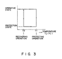
- Fig. 3 is a diagram for illustrating the temperature detection characteristic of the temperature detection circuit shown in Fig. 2 and shows the relation between the temperature Tj of the PN junction of the integrated circuit chip and the operative state of the acoustic power amplifier circuit.
- the thermal shielding circuit of the above construction it is possible to change the boundary condition between the protecting operation and the recovering operation of the power amplifier circuit by detecting that the amount of currents I3 and I5 has reached a preset value and changing the current I5 and thus provide a hysteresis characteristic with respect to temperature.
- the operation of the power amplifier circuit is interrupted when the first preset temperature T1 (for example, 150°C) is exceeded, and in a case where the temperature is changed from the high temperature to the low temperature, the protection operation is terminated when the temperature becomes lower than the second preset temperature T2 (for example, 100°C) which is sufficiently lower than the first preset temperature T1 so as to recover the normal operative state.
- the hysteresis width of the hysteresis characteristic can be easily set by adjusting the resistance of the resistor R4.
- the thermal shielding circuit can be prevented from being set into the oscillating state with the temperature of the integrated circuit chip kept at high temperatures equal to or near the preset temperature by repeatedly effecting the protecting operation and the recovering operation of the power amplifier circuit.
- the temperature characteristic of the thermal shielding circuit is determined by the temperature characteristic of the thermal voltage V T and the temperature characteristic of the resistors R7 and R8, influence by variation in the element characteristic on the preset temperature of the protection operation and the termination temperature of the protection operation can be sufficiently suppressed.
- the temperature detection circuit of this invention can be effectively used particularly in a case where a circuit such as an acoustic power amplifier circuit or a motor driver circuit which has a large power consumption is integrated.
Landscapes
- Physics & Mathematics (AREA)
- Engineering & Computer Science (AREA)
- General Physics & Mathematics (AREA)
- Microelectronics & Electronic Packaging (AREA)
- Power Engineering (AREA)
- Nonlinear Science (AREA)
- Electromagnetism (AREA)
- Radar, Positioning & Navigation (AREA)
- Automation & Control Theory (AREA)
- Amplifiers (AREA)
- Semiconductor Integrated Circuits (AREA)
- Measuring Temperature Or Quantity Of Heat (AREA)
- Control Of Electrical Variables (AREA)
- Measurement Of Current Or Voltage (AREA)
Applications Claiming Priority (2)
| Application Number | Priority Date | Filing Date | Title |
|---|---|---|---|
| JP2134940A JP2598154B2 (ja) | 1990-05-24 | 1990-05-24 | 温度検出回路 |
| JP134940/89 | 1990-05-24 |
Publications (3)
| Publication Number | Publication Date |
|---|---|
| EP0458332A2 true EP0458332A2 (fr) | 1991-11-27 |
| EP0458332A3 EP0458332A3 (en) | 1992-07-22 |
| EP0458332B1 EP0458332B1 (fr) | 1997-01-15 |
Family
ID=15140115
Family Applications (1)
| Application Number | Title | Priority Date | Filing Date |
|---|---|---|---|
| EP91108353A Expired - Lifetime EP0458332B1 (fr) | 1990-05-24 | 1991-05-23 | Montage de détection de la température utilisé dans un montage de protection thermique |
Country Status (5)
| Country | Link |
|---|---|
| US (1) | US5149199A (fr) |
| EP (1) | EP0458332B1 (fr) |
| JP (1) | JP2598154B2 (fr) |
| KR (1) | KR930006304B1 (fr) |
| DE (1) | DE69124138T2 (fr) |
Cited By (5)
| Publication number | Priority date | Publication date | Assignee | Title |
|---|---|---|---|---|
| EP0531615A3 (fr) * | 1991-08-09 | 1994-03-09 | Nec Corp | |
| WO1995012115A1 (fr) * | 1993-10-26 | 1995-05-04 | Analog Devices, Inc. | Transducteur thermique a deux bornes integrant une logique assurant la linearite du rapport entre le courant de fonctionnement et la temperature |
| US6310510B1 (en) | 1999-10-20 | 2001-10-30 | Telefonaktiebolaget Lm Ericsson (Publ) | Electronic circuit for producing a reference current independent of temperature and supply voltage |
| FR2857456A1 (fr) * | 2003-07-07 | 2005-01-14 | St Microelectronics Sa | Cellule de detection de temperature et procede de determination du seuil de detection d'une telle cellule |
| CN110068401A (zh) * | 2018-01-24 | 2019-07-30 | 三星电子株式会社 | 温度感测设备和温度-电压转换器 |
Families Citing this family (27)
| Publication number | Priority date | Publication date | Assignee | Title |
|---|---|---|---|---|
| US5359236A (en) * | 1993-05-25 | 1994-10-25 | Harris Corporation | Integrated circuit thermal sensor |
| JP2540753B2 (ja) * | 1993-09-01 | 1996-10-09 | 日本電気株式会社 | 過熱検出回路 |
| US7216064B1 (en) | 1993-09-21 | 2007-05-08 | Intel Corporation | Method and apparatus for programmable thermal sensor for an integrated circuit |
| JP3348576B2 (ja) * | 1995-11-10 | 2002-11-20 | ソニー株式会社 | 温度検出装置、これを搭載した半導体素子およびこれを用いたオートフォーカスシステム |
| US6055489A (en) * | 1997-04-15 | 2000-04-25 | Intel Corporation | Temperature measurement and compensation scheme |
| JP3338632B2 (ja) * | 1997-05-15 | 2002-10-28 | モトローラ株式会社 | 温度検出回路 |
| US6363490B1 (en) | 1999-03-30 | 2002-03-26 | Intel Corporation | Method and apparatus for monitoring the temperature of a processor |
| US6393374B1 (en) | 1999-03-30 | 2002-05-21 | Intel Corporation | Programmable thermal management of an integrated circuit die |
| US6789037B2 (en) * | 1999-03-30 | 2004-09-07 | Intel Corporation | Methods and apparatus for thermal management of an integrated circuit die |
| DE69933670D1 (de) * | 1999-08-31 | 2006-11-30 | St Microelectronics Srl | Temperaturfühler in Cmos-Technologie |
| US7263567B1 (en) | 2000-09-25 | 2007-08-28 | Intel Corporation | Method and apparatus for lowering the die temperature of a microprocessor and maintaining the temperature below the die burn out |
| KR100772594B1 (ko) * | 2001-06-30 | 2007-11-02 | 매그나칩 반도체 유한회사 | 온도 센서 |
| US6679628B2 (en) * | 2001-08-14 | 2004-01-20 | Schneider Automation Inc. | Solid state temperature measuring device and method |
| US6724665B2 (en) * | 2001-08-31 | 2004-04-20 | Matrix Semiconductor, Inc. | Memory device and method for selectable sub-array activation |
| US6735546B2 (en) * | 2001-08-31 | 2004-05-11 | Matrix Semiconductor, Inc. | Memory device and method for temperature-based control over write and/or read operations |
| GB2425419B (en) | 2002-10-01 | 2007-05-02 | Wolfson Microelectronics Plc | Temperature sensing apparatus and methods |
| JP2004146576A (ja) * | 2002-10-24 | 2004-05-20 | Renesas Technology Corp | 半導体温度測定回路 |
| US6954394B2 (en) * | 2002-11-27 | 2005-10-11 | Matrix Semiconductor, Inc. | Integrated circuit and method for selecting a set of memory-cell-layer-dependent or temperature-dependent operating conditions |
| US7057958B2 (en) * | 2003-09-30 | 2006-06-06 | Sandisk Corporation | Method and system for temperature compensation for memory cells with temperature-dependent behavior |
| US7218570B2 (en) * | 2004-12-17 | 2007-05-15 | Sandisk 3D Llc | Apparatus and method for memory operations using address-dependent conditions |
| US7332952B2 (en) * | 2005-11-23 | 2008-02-19 | Standard Microsystems Corporation | Accurate temperature measurement method for low beta transistors |
| US7283414B1 (en) | 2006-05-24 | 2007-10-16 | Sandisk 3D Llc | Method for improving the precision of a temperature-sensor circuit |
| US7896545B2 (en) * | 2008-03-19 | 2011-03-01 | Micron Technology, Inc. | Apparatus and methods for temperature calibration and sensing |
| WO2012046638A1 (fr) * | 2010-10-04 | 2012-04-12 | Ricoh Company, Ltd. | Elément électrique |
| JP7173661B2 (ja) * | 2018-11-16 | 2022-11-16 | ミネベアミツミ株式会社 | 湿度検出装置 |
| US11460428B2 (en) | 2018-11-16 | 2022-10-04 | Minebea Mitsumi Inc. | Humidity detecting device and method of determining malfunction |
| JP7167396B2 (ja) * | 2018-11-16 | 2022-11-09 | ミネベアミツミ株式会社 | 湿度検出装置及び故障判定方法 |
Family Cites Families (8)
| Publication number | Priority date | Publication date | Assignee | Title |
|---|---|---|---|---|
| US4350904A (en) * | 1980-09-22 | 1982-09-21 | Bell Telephone Laboratories, Incorporated | Current source with modified temperature coefficient |
| JPS58221507A (ja) * | 1982-06-18 | 1983-12-23 | Toshiba Corp | トランジスタ回路 |
| US4698655A (en) * | 1983-09-23 | 1987-10-06 | Motorola, Inc. | Overvoltage and overtemperature protection circuit |
| JPS6170805A (ja) * | 1984-09-14 | 1986-04-11 | Matsushita Electric Ind Co Ltd | 熱保護回路 |
| JPS6170806A (ja) * | 1984-09-14 | 1986-04-11 | Matsushita Electric Ind Co Ltd | 熱保護回路 |
| US4736125A (en) * | 1986-08-28 | 1988-04-05 | Applied Micro Circuits Corporation | Unbuffered TTL-to-ECL translator with temperature-compensated threshold voltage obtained from a constant-current reference voltage |
| US4789819A (en) * | 1986-11-18 | 1988-12-06 | Linear Technology Corporation | Breakpoint compensation and thermal limit circuit |
| GB2222884A (en) * | 1988-09-19 | 1990-03-21 | Philips Electronic Associated | Temperature sensing circuit |
-
1990
- 1990-05-24 JP JP2134940A patent/JP2598154B2/ja not_active Expired - Lifetime
-
1991
- 1991-05-20 KR KR1019910008153A patent/KR930006304B1/ko not_active Expired - Fee Related
- 1991-05-21 US US07/703,833 patent/US5149199A/en not_active Expired - Lifetime
- 1991-05-23 DE DE69124138T patent/DE69124138T2/de not_active Expired - Lifetime
- 1991-05-23 EP EP91108353A patent/EP0458332B1/fr not_active Expired - Lifetime
Cited By (8)
| Publication number | Priority date | Publication date | Assignee | Title |
|---|---|---|---|---|
| EP0531615A3 (fr) * | 1991-08-09 | 1994-03-09 | Nec Corp | |
| AU657441B2 (en) * | 1991-08-09 | 1995-03-09 | Nec Corporation | Temperature sensor circuit and constant-current circuit |
| WO1995012115A1 (fr) * | 1993-10-26 | 1995-05-04 | Analog Devices, Inc. | Transducteur thermique a deux bornes integrant une logique assurant la linearite du rapport entre le courant de fonctionnement et la temperature |
| US6310510B1 (en) | 1999-10-20 | 2001-10-30 | Telefonaktiebolaget Lm Ericsson (Publ) | Electronic circuit for producing a reference current independent of temperature and supply voltage |
| FR2857456A1 (fr) * | 2003-07-07 | 2005-01-14 | St Microelectronics Sa | Cellule de detection de temperature et procede de determination du seuil de detection d'une telle cellule |
| US7003424B2 (en) | 2003-07-07 | 2006-02-21 | Stmicroelectronics Sa | Temperature detection cell, and method to determine the detection threshold of such a cell |
| CN110068401A (zh) * | 2018-01-24 | 2019-07-30 | 三星电子株式会社 | 温度感测设备和温度-电压转换器 |
| CN110068401B (zh) * | 2018-01-24 | 2021-07-02 | 三星电子株式会社 | 温度感测设备和温度-电压转换器 |
Also Published As
| Publication number | Publication date |
|---|---|
| DE69124138D1 (de) | 1997-02-27 |
| KR910020420A (ko) | 1991-12-20 |
| KR930006304B1 (ko) | 1993-07-12 |
| EP0458332A3 (en) | 1992-07-22 |
| JP2598154B2 (ja) | 1997-04-09 |
| JPH0430609A (ja) | 1992-02-03 |
| DE69124138T2 (de) | 1997-06-05 |
| EP0458332B1 (fr) | 1997-01-15 |
| US5149199A (en) | 1992-09-22 |
Similar Documents
| Publication | Publication Date | Title |
|---|---|---|
| EP0458332A2 (fr) | Montage de détection de la température utilisé dans un montage de protection thermique | |
| JP3358459B2 (ja) | 温度検出回路 | |
| US4092693A (en) | Temperature sensing protection circuit for ic power chip having thermal hysteresis characteristic | |
| KR0136121B1 (ko) | 과열 검출 회로 | |
| JPH0683042B2 (ja) | 出力ドライバ回路 | |
| JP3081228B2 (ja) | 埋め込み型サーマルターンオフを有するイネーブル回路 | |
| US5206778A (en) | Sense circuit for on-chip thermal shutdown | |
| JPS59144208A (ja) | 集積回路の電力素子保護装置 | |
| US20250021122A1 (en) | Switch control voltage generator, bandgap reference generator, and method for generating switch voltage thereof | |
| JP2006013446A (ja) | 半導体回路 | |
| JP4395412B2 (ja) | 定電圧回路 | |
| JP3340345B2 (ja) | 定電圧発生回路 | |
| JP2543118B2 (ja) | 過熱遮断回路 | |
| JP4130856B2 (ja) | 電流源回路 | |
| JPH02248113A (ja) | 狭いしきい値変動範囲を有する過熱防止トリガ回路 | |
| JPH04344508A (ja) | 電圧/電流特性制御回路 | |
| JP3091520B2 (ja) | 定電圧回路 | |
| JP3403054B2 (ja) | 温度特性補正回路 | |
| KR920007364B1 (ko) | 열파손 방지회로 | |
| JP3265338B2 (ja) | 安定化電源回路 | |
| JP3675130B2 (ja) | 増幅回路 | |
| JPH0534028Y2 (fr) | ||
| JPH04313912A (ja) | 出力保護回路 | |
| JPH06121452A (ja) | 熱保護回路 | |
| JP3120580B2 (ja) | インピーダンス補償回路 |
Legal Events
| Date | Code | Title | Description |
|---|---|---|---|
| PUAI | Public reference made under article 153(3) epc to a published international application that has entered the european phase |
Free format text: ORIGINAL CODE: 0009012 |
|
| 17P | Request for examination filed |
Effective date: 19910523 |
|
| AK | Designated contracting states |
Kind code of ref document: A2 Designated state(s): DE FR GB |
|
| PUAL | Search report despatched |
Free format text: ORIGINAL CODE: 0009013 |
|
| AK | Designated contracting states |
Kind code of ref document: A3 Designated state(s): DE FR GB |
|
| RAP1 | Party data changed (applicant data changed or rights of an application transferred) |
Owner name: KABUSHIKI KAISHA TOSHIBA Owner name: TOSHIBA AVE CO., LTD |
|
| 17Q | First examination report despatched |
Effective date: 19941111 |
|
| GRAG | Despatch of communication of intention to grant |
Free format text: ORIGINAL CODE: EPIDOS AGRA |
|
| GRAH | Despatch of communication of intention to grant a patent |
Free format text: ORIGINAL CODE: EPIDOS IGRA |
|
| RAP1 | Party data changed (applicant data changed or rights of an application transferred) |
Owner name: KABUSHIKI KAISHA TOSHIBA Owner name: TOSHIBA AVE CO., LTD Owner name: TOSHIBA MICRO-ELECTRONICS CORPORATION |
|
| GRAH | Despatch of communication of intention to grant a patent |
Free format text: ORIGINAL CODE: EPIDOS IGRA |
|
| GRAA | (expected) grant |
Free format text: ORIGINAL CODE: 0009210 |
|
| AK | Designated contracting states |
Kind code of ref document: B1 Designated state(s): DE FR GB |
|
| REF | Corresponds to: |
Ref document number: 69124138 Country of ref document: DE Date of ref document: 19970227 |
|
| PGFP | Annual fee paid to national office [announced via postgrant information from national office to epo] |
Ref country code: FR Payment date: 19970513 Year of fee payment: 7 |
|
| PGFP | Annual fee paid to national office [announced via postgrant information from national office to epo] |
Ref country code: GB Payment date: 19970514 Year of fee payment: 7 |
|
| ET | Fr: translation filed | ||
| PLBE | No opposition filed within time limit |
Free format text: ORIGINAL CODE: 0009261 |
|
| STAA | Information on the status of an ep patent application or granted ep patent |
Free format text: STATUS: NO OPPOSITION FILED WITHIN TIME LIMIT |
|
| 26N | No opposition filed | ||
| PG25 | Lapsed in a contracting state [announced via postgrant information from national office to epo] |
Ref country code: GB Free format text: LAPSE BECAUSE OF NON-PAYMENT OF DUE FEES Effective date: 19980523 |
|
| PG25 | Lapsed in a contracting state [announced via postgrant information from national office to epo] |
Ref country code: FR Free format text: LAPSE BECAUSE OF NON-PAYMENT OF DUE FEES Effective date: 19980531 |
|
| GBPC | Gb: european patent ceased through non-payment of renewal fee |
Effective date: 19980523 |
|
| REG | Reference to a national code |
Ref country code: FR Ref legal event code: ST |
|
| PGFP | Annual fee paid to national office [announced via postgrant information from national office to epo] |
Ref country code: DE Payment date: 20100519 Year of fee payment: 20 |
|
| REG | Reference to a national code |
Ref country code: DE Ref legal event code: R071 Ref document number: 69124138 Country of ref document: DE |
|
| PG25 | Lapsed in a contracting state [announced via postgrant information from national office to epo] |
Ref country code: DE Free format text: LAPSE BECAUSE OF EXPIRATION OF PROTECTION Effective date: 20110524 |