EP0458381A2 - Halbleiteranordnung mit einem Hochspannungs-MOS-Transistor mit einem abgeschirmten Überkreuzungspfad für einen Hochspannungsverbindungsbus - Google Patents
Halbleiteranordnung mit einem Hochspannungs-MOS-Transistor mit einem abgeschirmten Überkreuzungspfad für einen Hochspannungsverbindungsbus Download PDFInfo
- Publication number
- EP0458381A2 EP0458381A2 EP91201096A EP91201096A EP0458381A2 EP 0458381 A2 EP0458381 A2 EP 0458381A2 EP 91201096 A EP91201096 A EP 91201096A EP 91201096 A EP91201096 A EP 91201096A EP 0458381 A2 EP0458381 A2 EP 0458381A2
- Authority
- EP
- European Patent Office
- Prior art keywords
- gate
- source
- drain
- connection bus
- disjuncture
- Prior art date
- Legal status (The legal status is an assumption and is not a legal conclusion. Google has not performed a legal analysis and makes no representation as to the accuracy of the status listed.)
- Granted
Links
Images



Classifications
-
- H—ELECTRICITY
- H10—SEMICONDUCTOR DEVICES; ELECTRIC SOLID-STATE DEVICES NOT OTHERWISE PROVIDED FOR
- H10D—INORGANIC ELECTRIC SEMICONDUCTOR DEVICES
- H10D30/00—Field-effect transistors [FET]
- H10D30/60—Insulated-gate field-effect transistors [IGFET]
- H10D30/64—Double-diffused metal-oxide semiconductor [DMOS] FETs
- H10D30/65—Lateral DMOS [LDMOS] FETs
-
- H—ELECTRICITY
- H10—SEMICONDUCTOR DEVICES; ELECTRIC SOLID-STATE DEVICES NOT OTHERWISE PROVIDED FOR
- H10D—INORGANIC ELECTRIC SEMICONDUCTOR DEVICES
- H10D30/00—Field-effect transistors [FET]
- H10D30/60—Insulated-gate field-effect transistors [IGFET]
- H10D30/64—Double-diffused metal-oxide semiconductor [DMOS] FETs
- H10D30/66—Vertical DMOS [VDMOS] FETs
- H10D30/668—Vertical DMOS [VDMOS] FETs having trench gate electrodes, e.g. UMOS transistors
-
- H—ELECTRICITY
- H10—SEMICONDUCTOR DEVICES; ELECTRIC SOLID-STATE DEVICES NOT OTHERWISE PROVIDED FOR
- H10D—INORGANIC ELECTRIC SEMICONDUCTOR DEVICES
- H10D62/00—Semiconductor bodies, or regions thereof, of devices having potential barriers
- H10D62/10—Shapes, relative sizes or dispositions of the regions of the semiconductor bodies; Shapes of the semiconductor bodies
- H10D62/124—Shapes, relative sizes or dispositions of the regions of semiconductor bodies or of junctions between the regions
- H10D62/126—Top-view geometrical layouts of the regions or the junctions
- H10D62/127—Top-view geometrical layouts of the regions or the junctions of cellular field-effect devices, e.g. multicellular DMOS transistors or IGBTs
-
- H—ELECTRICITY
- H10—SEMICONDUCTOR DEVICES; ELECTRIC SOLID-STATE DEVICES NOT OTHERWISE PROVIDED FOR
- H10D—INORGANIC ELECTRIC SEMICONDUCTOR DEVICES
- H10D64/00—Electrodes of devices having potential barriers
- H10D64/111—Field plates
- H10D64/112—Field plates comprising multiple field plate segments
-
- H—ELECTRICITY
- H10—SEMICONDUCTOR DEVICES; ELECTRIC SOLID-STATE DEVICES NOT OTHERWISE PROVIDED FOR
- H10W—GENERIC PACKAGES, INTERCONNECTIONS, CONNECTORS OR OTHER CONSTRUCTIONAL DETAILS OF DEVICES COVERED BY CLASS H10
- H10W20/00—Interconnections in chips, wafers or substrates
- H10W20/40—Interconnections external to wafers or substrates, e.g. back-end-of-line [BEOL] metallisations or vias connecting to gate electrodes
- H10W20/495—Capacitive arrangements or effects of, or between wiring layers
-
- H—ELECTRICITY
- H10—SEMICONDUCTOR DEVICES; ELECTRIC SOLID-STATE DEVICES NOT OTHERWISE PROVIDED FOR
- H10D—INORGANIC ELECTRIC SEMICONDUCTOR DEVICES
- H10D62/00—Semiconductor bodies, or regions thereof, of devices having potential barriers
- H10D62/10—Shapes, relative sizes or dispositions of the regions of the semiconductor bodies; Shapes of the semiconductor bodies
- H10D62/17—Semiconductor regions connected to electrodes not carrying current to be rectified, amplified or switched, e.g. channel regions
- H10D62/393—Body regions of DMOS transistors or IGBTs
Definitions
- the invention relates to a semiconductor device with a high voltage field effect transistor comprising a source, a gate and a drain, a charge carrier drift zone at the surface thereof extending from the gate to the drain and comprising respective electrodes for the source, gate and drain, in which a first dielectric layer covers the drift zone and an elongated high voltage connection bus extends over said dielectric layer to the drain electrode, and particularly to a semiconductor device with a field effect transistor having a closed layout plan wherein the drain is laterally surrounded by the source and the gate so that a high voltage connection bus for the drain must traverse a path which crosses the drift zone.
- field effect transistor refers particularly to a transistor having a source, a drain and a gate, the gate electrode extending over a dielectric layer, for example silicon oxide or nitride, at the surface of the transistor; the gate electrode when energized causing either enhancement or depletion of charge carriers in an underlying surface channel of the transistor which constitutes the gate between the source and the drain.
- the present invention aims to counteract the influence of the electric field produced by the connection bus on the charge carriers in the drift region lying underneath it.
- a semiconductor device in accordance with the invention is characterized in that, a plurality of electrically conductive strips are arranged in succession on said first dielectric layer to form a crossover path, in that said strips extend substantially transversely to the direction of said crossover path and have a length substantially exceeding the width of said connection bus and a width not exceeding the width of the connection bus, in that the strips are covered by a second dielectric layer and in that the connection bus extends over said crossover path supported on said second dielectric layer.
- each strip of the crossover path forms a coupling capacitance C ci with said connection bus and further a coupling capacitance C di with said drift zone.
- the area of the capacitance C di is several times larger than that of capacitance C ci while the thicknesses of the first and second dielectric layer may be approximately equal.
- the capacitance value of the capacitance C di will be several times larger than the capacitance value of the capacitance C ci .
- the transistor has a closed layout plan, preferably a substantially rectangular partially interleaved layout, wherein the drain is laterally surrounded by the source and gate.
- the connection bus will have to cross the drift region and the gate and source with respect to which it may have a potential difference of the order of several hundred Volts.
- said gate and source electrodes are provided with a disjuncture forming a gap through which said connection bus extends. Due to the invention the connection bus can safely be applied since its electric field is effectively shielded by the crossover path.
- Fig. 1 is shown a cross-section of the structure of a high voltage lateral double diffused N-channel enhancement mode MOS transistor (i.e., an LDMOS transistor), substantially as set forth in the above-referenced U.S. Patent No. 4,300,150, which is hereby incorporated by reference.
- the silicon substrate 10 is of lightly doped P-type conductivity, with an epitaxial N-type surface layer 12 therein. Diffused into a surface portion of such epitaxial layer and bounding it is a P-type zone 16 forming a P-N junction 17 therewith, and diffused into a surface portion of zone 16 is an N-type zone which constitutes the source 14.
- P-type zone 16 which extends beyond source 14 forms a channel at the surface which constitutes the gate 18.
- a diffused N-type zone which constitutes the drain 20.
- a silicon oxide surface layer 22 is formed over epitaxial layer 12, extending over a portion of drain 20 and also, with reduced thickness, over gate 18 and a portion of source 14.
- a charge carrier drift zone 21 extends in a surface portion of epitaxial layer 12 between gate 18 and drain 20.
- a metallized source electrode 26 is formed over the surface portion of source 14 not covered by oxide layer 22, and also extends over the portion of P-type zone 16 which continues past source 14. Source electrode 26 is therefore in ohmic connection with the P-type substrate, so that the source and substrate will be at the same potential. This is typical of high voltage MOS transistors, the source and substrate both being grounded.
- a metallized drain electrode 28 is formed over drain 20. The electric field produced by the drain potential will therefore linearly decrease along the length of the drift zone from drain 20 to gate 18.
- an ion-implanted buried P+ region 30a has been provided at the junction between substrate 10 and epitaxial layer 12 in the vicinity of P-type region 16. This serves to reduce the field intensity at the junction of region 16 with epitaxial layer 12, thereby further enhancing the reverse breakdown voltage of the transistor.
- Fig. 2 shows the layout plan of the transistor shown in cross-section in Fig. 1.
- Such plan is substantially rectangular, but has a finger-like interleaved portion at the lower end thereof to achieve increased effective lengths of the source, gate and drain and, consequently, increased power and lower resistance ratings of the transistor.
- a cross-section taken at 1-1 in Fig. 2 will be as shown in Fig. 1, and the identifying numerals in Fig. 2 correspond to those in Fig. 1.
- the drain electrode 28 is surrounded by the gate and source electrodes 24 and 26, which are around the periphery of the layout plan, and has downwardly extending fingers which interleave with upwardly extending fingers of the source and gate electrodes at the bottom of the layout.
- the source and gate electrodes, and the underlying source zone 14 and gate zone 18 (not visible), are maintained at a constant spacing from drain electrode 28 and the underlying drain zone 20 (not visible) over the entire layout, such spacing being where the drift zone 21 (not visible) exists under the oxide layer 22.
- a metal contact pad 31 is in electrical contact with source electrode 26.
- Another metal contact pad 32 is in electrical contact with gate electrode 24, reaching it through a gap provided for that purpose in source electrode 26.
- a third contact pad 33, for connection to an external high voltage connection bus, is in electrical contact with drain electrode 28. It is clear from Fig. 2 that in order for an external high voltage connection bus in a parallel plane to reach drain contact pad 33, it must cross over the source and gate electrodes and extend over the drift zone.
- FIG. 3 there is shown the electric field distribution produced in drift zone 21 of the transistor in Fig. 1 when the drain is at a potential of 500V relative to the source. It is this field distribution that should be preserved despite the presence of the electrical field produced by a high voltage connection bus extending in a parallel plane over drift zone 21 and across gate and source electrodes 24 and 26.
- Fig. 4 is a projection view of the basic structure of the transistor in accordance with the invention, and elements therein the same as those in Fig. 1 have the same reference numerals. It is seen that on the oxide layer 22 over the drift zone, between gate electrode 24 and drain electrode 28, there is provided a succession of conductive strips 34, 35...n, forming a crossover path between the gate and drain electrodes, such strips extending in a direction transverse to such crossover path. They may be of doped polycrystalline silicon (“polysilicon”), and are floating in potential since they are electrically unconnected. As many such strips as possible should be included in order for each strip to intercept only a substantially constant incremental portion of the changing electric field distribution along the length of drift zone 21, as shown in Fig. 3.
- polysilicon doped polycrystalline silicon
- the distance between the gate and drain electrodes may typically be about 24 microns, and the minimum width of a polysilicon strip is about 2 microns. Since spacing is necessary between the strips, this leaves room for no more than 10 strips.
- the significance of such conductive strips can be understood with reference to Fig. 4a, showing the equivalent coupling capacitances which are formed by such strips and the electric field distribution in drift zone 21.
- v di is the potential of the drift zone at the ith strip
- v pi is the potential of such strip.
- the capacitance C di between such strip and the underlying portion of the drift zone will therefore be where K is a constant given by the permittivity of the oxide layer 22 over drift zone 21 in Fig.
- the transistor therein is the same as in Fig. 4 but further includes an external high voltage connection bus 36 extending in a plane parallel to the surface of the transistor and connected to drain electrode 28.
- a dielectric coating such as an oxide deposited from a low temperature plasma (LTO) is formed on the conductive strips.
- LTO low temperature plasma
- the elongated metallic connection bus 36 traverses the crossover path formed by such strips, in contact with the oxide layer thereon.
- the gate and source electrodes 24 and 26 have a disjuncture therein, as shown, forming a gap which bus 36 traverses.
- the capacitance C ci is given by where w i is the width of high voltage bus 33 and t i is the thickness of the coating layer on the conductive strips. Since the bus width w i is much less than the strip length l s , and the thicknesses t ox and t i are approximately equal, comparison of equations (1) and (3) shows that C ci will be much smaller than C di and so from equation (2) v p will be approximately zero. This means that the conductive strips will be substantially at the same potential as the underlying portion of drift zone 21, so that drift zone 21 is effectively shielded from the electric field produced by the connection bus 36.
- the present invention can employ either of two alternative embodiments.
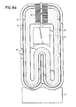
- the first is to extend the length of the transistor to provide more conductive strips along the path formed thereby between the drain and gate electrodes, and a layout plan in accordance with that embodiment is shown in Figure 6a.
- the second embodiment is to position the high voltage connection bus at a corner of a rectangular layout plan and to provide a curvilinear shoulder on the adjacent portion of the drain electrode, thereby providing an extended length of the drift zone at such corner without increasing the area of the transistor.
- the high voltage bus 36 is connected to drain contact pad 33 and traverses a gap in the gate and source electrodes 24 and 26 at the top of the layout where a disjuncture has been provided therein as described above with reference to Figure 5.
- the upper portion of the layout has been extended to increase the length of the drift zone in that region, thereby enabling a larger number of conductive strips 40 to be included between gate electrode 24 and drain electrode 28 along the crossover path traversed by connection bus 36.
- the drift zone may be 45 microns except in the region at the top of the layout where it has been extended to 75 microns. With a strip width of 2 to 3 microns, this permits about 43 conductive strips in the crossover path followed by the connection bus over the drift zone.
- the high voltage connection bus extends to drain contact pad 33 through a gap at one corner of the gate and source electrodes 24 and 26.
- the length of the drift zone at such corner is considerably increased. Consequently, a lesser or possibly no extension of the layout may still provide enough space between the gate and source electrodes for a sufficient number of conductive strips to achieve adequate shielding of the drift zone from the electric field produced by the connection bus.
- Figure 7 shows how a disjuncture may be formed in the gate and source electrodes to provide a gap for traversal by the high voltage connection bus.
- the N-type drift zone is thereby effectively terminated by the diode junction which exists between it and the P-type zone 16.
- An oxide coating is deposited on the exposed surfaces of zones 16 and 18, and the sequence of conductive strips 40 is continued across such oxide layer.
- a high voltage transistor having a substantially rectangular layout plan which is extended as in Figure 6a was constructed with a crossover path of two alternating types of doped polysilicon strips.
- C ci was 1.55 x 10 ⁇ 15 F and C di was 1.2 x 10 ⁇ 14 F
- C ci was 1.3 x 10 ⁇ 15 F and C di was 7.6 x 10 ⁇ 14 F.
- the first series of strips were oxidized after deposition and patterning, enabling the second series to be placed close to or even overlapping the strips in the first series without danger of short-circuiting them.
- Such transistor also had the following further parameters: drift zone 21:45 microns, extended at the top to 120 microns; oxide layer 22: 0.85 microns thick over drift zone 21; polysilicon strips: 43 strips spaced at 0.25 microns and with an oxide layer thereon of 1 micron; the first type were each 100 microns long and 3 microns wide, and the second type were each 75 microns long and 2.5 microns wide; interconnect bus: a rectangular metal strip 15 microns wide and 1 micron thick.
- the MOS transistor could conceivably have a circular layout plan, but a rectangular or substantially rectangular (such as elliptical) layout is preferable because it can be extended in only a single region. Extension of a circular layout would require an unnecessary increase in the total area of the transistor since an extended length of the drift zone is only necessary along the crossover path traversed by the connection bus.
Landscapes
- Insulated Gate Type Field-Effect Transistor (AREA)
- Internal Circuitry In Semiconductor Integrated Circuit Devices (AREA)
Applications Claiming Priority (2)
| Application Number | Priority Date | Filing Date | Title |
|---|---|---|---|
| US07/525,288 US5040045A (en) | 1990-05-17 | 1990-05-17 | High voltage MOS transistor having shielded crossover path for a high voltage connection bus |
| US525288 | 1990-05-17 |
Publications (3)
| Publication Number | Publication Date |
|---|---|
| EP0458381A2 true EP0458381A2 (de) | 1991-11-27 |
| EP0458381A3 EP0458381A3 (de) | 1991-12-11 |
| EP0458381B1 EP0458381B1 (de) | 1996-03-27 |
Family
ID=24092646
Family Applications (1)
| Application Number | Title | Priority Date | Filing Date |
|---|---|---|---|
| EP91201096A Expired - Lifetime EP0458381B1 (de) | 1990-05-17 | 1991-05-08 | Halbleiteranordnung mit einem Hochspannungs-MOS-Transistor mit einem abgeschirmten Überkreuzungspfad für einen Hochspannungsverbindungsbus |
Country Status (4)
| Country | Link |
|---|---|
| US (1) | US5040045A (de) |
| EP (1) | EP0458381B1 (de) |
| JP (1) | JPH0770729B2 (de) |
| DE (1) | DE69118242T2 (de) |
Cited By (4)
| Publication number | Priority date | Publication date | Assignee | Title |
|---|---|---|---|---|
| WO1998049732A3 (en) * | 1997-04-28 | 1999-02-04 | Koninkl Philips Electronics Nv | Lateral mos transistor device |
| EP1111683A3 (de) * | 1999-12-17 | 2005-02-02 | Matsushita Electric Industrial Co., Ltd. | Hochspannungshalbleiteranordnung |
| DE102006033692A1 (de) * | 2006-07-20 | 2008-01-31 | Austriamicrosystems Ag | Strukturiertes Dielektrikum für LDMOS-Transistor und Verfahren zur Herstellung |
| DE10255116B4 (de) * | 2002-11-26 | 2015-04-02 | Infineon Technologies Ag | LDMOS-Transistor und Verfahren zu dessen Herstellung |
Families Citing this family (71)
| Publication number | Priority date | Publication date | Assignee | Title |
|---|---|---|---|---|
| US5258636A (en) * | 1991-12-12 | 1993-11-02 | Power Integrations, Inc. | Narrow radius tips for high voltage semiconductor devices with interdigitated source and drain electrodes |
| JP2739004B2 (ja) * | 1992-01-16 | 1998-04-08 | 三菱電機株式会社 | 半導体装置 |
| DE69415987T2 (de) * | 1994-11-08 | 1999-06-24 | Stmicroelectronics S.R.L., Agrate Brianza, Mailand/Milano | Integrierte Anordnung mit einer Struktur zum Schutz gegen hohe elektrische Felder |
| JP3291958B2 (ja) * | 1995-02-21 | 2002-06-17 | 富士電機株式会社 | バックソースmosfet |
| JP3808116B2 (ja) * | 1995-04-12 | 2006-08-09 | 富士電機デバイステクノロジー株式会社 | 高耐圧ic |
| EP0738011B1 (de) | 1995-04-12 | 2014-12-10 | Fuji Electric Co., Ltd. | Integrierter Hochspannungsschaltkreis, Hochspannungsübergangsabschluss- struktur und MIS-Hochspannungstransistor |
| EP0772241B1 (de) | 1995-10-30 | 2004-06-09 | STMicroelectronics S.r.l. | Leistungsbauteil hoher Dichte in MOS-Technologie |
| EP0772242B1 (de) | 1995-10-30 | 2006-04-05 | STMicroelectronics S.r.l. | Leistungsbauteil in MOS-Technologie mit einer einzelnen kritischen Grösse |
| US6043126A (en) * | 1996-10-25 | 2000-03-28 | International Rectifier Corporation | Process for manufacture of MOS gated device with self aligned cells |
| EP0961325B1 (de) * | 1998-05-26 | 2008-05-07 | STMicroelectronics S.r.l. | MOS-Technologie-Leistungsanordnung mit hoher Integrationsdichte |
| US6084277A (en) * | 1999-02-18 | 2000-07-04 | Power Integrations, Inc. | Lateral power MOSFET with improved gate design |
| US6614088B1 (en) * | 2000-02-18 | 2003-09-02 | James D. Beasom | Breakdown improvement method and sturcture for lateral DMOS device |
| JP3776666B2 (ja) | 2000-02-25 | 2006-05-17 | 沖電気工業株式会社 | 半導体装置 |
| US6635926B2 (en) * | 2000-08-30 | 2003-10-21 | Shindengen Electric Manufacturing Co., Ltd. | Field effect transistor with high withstand voltage and low resistance |
| US6509220B2 (en) | 2000-11-27 | 2003-01-21 | Power Integrations, Inc. | Method of fabricating a high-voltage transistor |
| US6768171B2 (en) | 2000-11-27 | 2004-07-27 | Power Integrations, Inc. | High-voltage transistor with JFET conduction channels |
| US6424007B1 (en) | 2001-01-24 | 2002-07-23 | Power Integrations, Inc. | High-voltage transistor with buried conduction layer |
| JP2002270830A (ja) * | 2001-03-12 | 2002-09-20 | Fuji Electric Co Ltd | 半導体装置 |
| US7786533B2 (en) * | 2001-09-07 | 2010-08-31 | Power Integrations, Inc. | High-voltage vertical transistor with edge termination structure |
| US6573558B2 (en) * | 2001-09-07 | 2003-06-03 | Power Integrations, Inc. | High-voltage vertical transistor with a multi-layered extended drain structure |
| US6555873B2 (en) * | 2001-09-07 | 2003-04-29 | Power Integrations, Inc. | High-voltage lateral transistor with a multi-layered extended drain structure |
| US6635544B2 (en) * | 2001-09-07 | 2003-10-21 | Power Intergrations, Inc. | Method of fabricating a high-voltage transistor with a multi-layered extended drain structure |
| US7221011B2 (en) * | 2001-09-07 | 2007-05-22 | Power Integrations, Inc. | High-voltage vertical transistor with a multi-gradient drain doping profile |
| JP4667756B2 (ja) * | 2004-03-03 | 2011-04-13 | 三菱電機株式会社 | 半導体装置 |
| US8653583B2 (en) | 2007-02-16 | 2014-02-18 | Power Integrations, Inc. | Sensing FET integrated with a high-voltage transistor |
| US7859037B2 (en) * | 2007-02-16 | 2010-12-28 | Power Integrations, Inc. | Checkerboarded high-voltage vertical transistor layout |
| US7595523B2 (en) | 2007-02-16 | 2009-09-29 | Power Integrations, Inc. | Gate pullback at ends of high-voltage vertical transistor structure |
| US7468536B2 (en) | 2007-02-16 | 2008-12-23 | Power Integrations, Inc. | Gate metal routing for transistor with checkerboarded layout |
| US7557406B2 (en) * | 2007-02-16 | 2009-07-07 | Power Integrations, Inc. | Segmented pillar layout for a high-voltage vertical transistor |
| JP4772843B2 (ja) * | 2008-09-17 | 2011-09-14 | シャープ株式会社 | 半導体装置及びその製造方法 |
| US20110241114A1 (en) * | 2010-04-02 | 2011-10-06 | Taiwan Semiconductor Manufacturing Company, Ltd. | High voltage mos transistor |
| US8618627B2 (en) | 2010-06-24 | 2013-12-31 | Fairchild Semiconductor Corporation | Shielded level shift transistor |
| TWI449159B (zh) | 2011-04-18 | 2014-08-11 | Episil Technologies Inc | 功率橫向雙擴散金氧半導體元件 |
| US8643101B2 (en) | 2011-04-20 | 2014-02-04 | United Microelectronics Corp. | High voltage metal oxide semiconductor device having a multi-segment isolation structure |
| US8581338B2 (en) | 2011-05-12 | 2013-11-12 | United Microelectronics Corp. | Lateral-diffused metal oxide semiconductor device (LDMOS) and fabrication method thereof |
| CN102185805B (zh) * | 2011-05-17 | 2013-11-13 | 惠州市奥罗拉科技有限公司 | 一种m-bus总线驱动电路 |
| US8501603B2 (en) | 2011-06-15 | 2013-08-06 | United Microelectronics Corp. | Method for fabricating high voltage transistor |
| US8592905B2 (en) | 2011-06-26 | 2013-11-26 | United Microelectronics Corp. | High-voltage semiconductor device |
| US20130043513A1 (en) | 2011-08-19 | 2013-02-21 | United Microelectronics Corporation | Shallow trench isolation structure and fabricating method thereof |
| US8729599B2 (en) | 2011-08-22 | 2014-05-20 | United Microelectronics Corp. | Semiconductor device |
| US8921937B2 (en) | 2011-08-24 | 2014-12-30 | United Microelectronics Corp. | High voltage metal-oxide-semiconductor transistor device and method of fabricating the same |
| CN103094317B (zh) * | 2011-11-01 | 2015-10-14 | 上海华虹宏力半导体制造有限公司 | 隔离型高耐压场效应管的版图结构 |
| US8742498B2 (en) | 2011-11-03 | 2014-06-03 | United Microelectronics Corp. | High voltage semiconductor device and fabricating method thereof |
| US8482063B2 (en) | 2011-11-18 | 2013-07-09 | United Microelectronics Corporation | High voltage semiconductor device |
| CN103123929B (zh) * | 2011-11-21 | 2015-10-14 | 上海华虹宏力半导体制造有限公司 | 隔离型高耐压场效应管的版图结构 |
| US8587058B2 (en) | 2012-01-02 | 2013-11-19 | United Microelectronics Corp. | Lateral diffused metal-oxide-semiconductor device |
| US8492835B1 (en) | 2012-01-20 | 2013-07-23 | United Microelectronics Corporation | High voltage MOSFET device |
| US9093296B2 (en) | 2012-02-09 | 2015-07-28 | United Microelectronics Corp. | LDMOS transistor having trench structures extending to a buried layer |
| TWI523196B (zh) | 2012-02-24 | 2016-02-21 | 聯華電子股份有限公司 | 高壓金氧半導體電晶體元件及其佈局圖案 |
| US8890144B2 (en) | 2012-03-08 | 2014-11-18 | United Microelectronics Corp. | High voltage semiconductor device |
| US9236471B2 (en) | 2012-04-24 | 2016-01-12 | United Microelectronics Corp. | Semiconductor structure and method for manufacturing the same |
| US9159791B2 (en) | 2012-06-06 | 2015-10-13 | United Microelectronics Corp. | Semiconductor device comprising a conductive region |
| US8836067B2 (en) | 2012-06-18 | 2014-09-16 | United Microelectronics Corp. | Transistor device and manufacturing method thereof |
| US8674441B2 (en) | 2012-07-09 | 2014-03-18 | United Microelectronics Corp. | High voltage metal-oxide-semiconductor transistor device |
| US8643104B1 (en) | 2012-08-14 | 2014-02-04 | United Microelectronics Corp. | Lateral diffusion metal oxide semiconductor transistor structure |
| US8729631B2 (en) | 2012-08-28 | 2014-05-20 | United Microelectronics Corp. | MOS transistor |
| US9196717B2 (en) | 2012-09-28 | 2015-11-24 | United Microelectronics Corp. | High voltage metal-oxide-semiconductor transistor device |
| US8829611B2 (en) | 2012-09-28 | 2014-09-09 | United Microelectronics Corp. | High voltage metal-oxide-semiconductor transistor device |
| US8704304B1 (en) | 2012-10-05 | 2014-04-22 | United Microelectronics Corp. | Semiconductor structure |
| US20140110777A1 (en) | 2012-10-18 | 2014-04-24 | United Microelectronics Corp. | Trench gate metal oxide semiconductor field effect transistor and fabricating method thereof |
| US9224857B2 (en) | 2012-11-12 | 2015-12-29 | United Microelectronics Corp. | Semiconductor structure and method for manufacturing the same |
| US9035425B2 (en) | 2013-05-02 | 2015-05-19 | United Microelectronics Corp. | Semiconductor integrated circuit |
| US8896057B1 (en) | 2013-05-14 | 2014-11-25 | United Microelectronics Corp. | Semiconductor structure and method for manufacturing the same |
| US8786362B1 (en) | 2013-06-04 | 2014-07-22 | United Microelectronics Corporation | Schottky diode having current leakage protection structure and current leakage protecting method of the same |
| US8941175B2 (en) | 2013-06-17 | 2015-01-27 | United Microelectronics Corp. | Power array with staggered arrangement for improving on-resistance and safe operating area |
| US9660053B2 (en) | 2013-07-12 | 2017-05-23 | Power Integrations, Inc. | High-voltage field-effect transistor having multiple implanted layers |
| US9136375B2 (en) | 2013-11-21 | 2015-09-15 | United Microelectronics Corp. | Semiconductor structure |
| US10325988B2 (en) | 2013-12-13 | 2019-06-18 | Power Integrations, Inc. | Vertical transistor device structure with cylindrically-shaped field plates |
| US9543396B2 (en) | 2013-12-13 | 2017-01-10 | Power Integrations, Inc. | Vertical transistor device structure with cylindrically-shaped regions |
| US9490360B2 (en) | 2014-02-19 | 2016-11-08 | United Microelectronics Corp. | Semiconductor device and operating method thereof |
| CN104465722B (zh) * | 2014-12-09 | 2017-06-06 | 上海华虹宏力半导体制造有限公司 | 高压隔离环结构 |
Family Cites Families (13)
| Publication number | Priority date | Publication date | Assignee | Title |
|---|---|---|---|---|
| JPS538080A (en) * | 1977-03-28 | 1978-01-25 | Toshiba Corp | Insulated gate type field effect transistor |
| IT1111981B (it) * | 1979-02-13 | 1986-01-13 | Ates Componenti Elettron | Struttura di transistore v(br)ceo protetto per il caso di inversione delle polarita' di alimentazione e prodotto risultante |
| JPS567479A (en) * | 1979-06-29 | 1981-01-26 | Toshiba Corp | Field-effect type semiconductor device |
| JPS5638867A (en) * | 1979-09-07 | 1981-04-14 | Hitachi Ltd | Insulated gate type field effect transistor |
| JPS56133871A (en) * | 1980-03-22 | 1981-10-20 | Sharp Corp | Mos field effect semiconductor device with high breakdown voltage |
| JPS56169368A (en) * | 1980-05-30 | 1981-12-26 | Sharp Corp | High withstand voltage mos field effect semiconductor device |
| US4300150A (en) * | 1980-06-16 | 1981-11-10 | North American Philips Corporation | Lateral double-diffused MOS transistor device |
| US4654680A (en) * | 1980-09-24 | 1987-03-31 | Semiconductor Energy Laboratory Co., Ltd. | Sidewall gate IGFET |
| US4430583A (en) * | 1981-10-30 | 1984-02-07 | Bell Telephone Laboratories, Incorporated | Apparatus for increasing the speed of a circuit having a string of IGFETs |
| US4651186A (en) * | 1981-11-18 | 1987-03-17 | Mitsubishi Denki Kabushiki Kaisha | Field effect transistor with improved withstand voltage characteristic |
| JPS613458A (ja) * | 1984-06-15 | 1986-01-09 | Nec Corp | Misトランジスタ |
| JPS61168253A (ja) * | 1985-01-19 | 1986-07-29 | Sharp Corp | 高耐圧mos電界効果半導体装置 |
| US4881106A (en) * | 1988-05-23 | 1989-11-14 | Ixys Corporation | DV/DT of power MOSFETS |
-
1990
- 1990-05-17 US US07/525,288 patent/US5040045A/en not_active Expired - Lifetime
-
1991
- 1991-05-08 EP EP91201096A patent/EP0458381B1/de not_active Expired - Lifetime
- 1991-05-08 DE DE69118242T patent/DE69118242T2/de not_active Expired - Fee Related
- 1991-05-17 JP JP3140692A patent/JPH0770729B2/ja not_active Expired - Fee Related
Non-Patent Citations (1)
| Title |
|---|
| EXTENDED ABSTRACTS. vol. 87-1, no. 1, 1987, PRINCETON, NEW JERSEY US pages 161 - 162; M. AMATO: 'Reduced electric field crwoding at the fingertips of lateral DMOS transistors ' * |
Cited By (5)
| Publication number | Priority date | Publication date | Assignee | Title |
|---|---|---|---|---|
| WO1998049732A3 (en) * | 1997-04-28 | 1999-02-04 | Koninkl Philips Electronics Nv | Lateral mos transistor device |
| EP1111683A3 (de) * | 1999-12-17 | 2005-02-02 | Matsushita Electric Industrial Co., Ltd. | Hochspannungshalbleiteranordnung |
| DE10255116B4 (de) * | 2002-11-26 | 2015-04-02 | Infineon Technologies Ag | LDMOS-Transistor und Verfahren zu dessen Herstellung |
| DE102006033692A1 (de) * | 2006-07-20 | 2008-01-31 | Austriamicrosystems Ag | Strukturiertes Dielektrikum für LDMOS-Transistor und Verfahren zur Herstellung |
| DE102006033692B4 (de) * | 2006-07-20 | 2011-01-05 | Austriamicrosystems Ag | Verfahren zur Herstellung eines strukturierten Dielektrikums für einen LDMOS-Transistor |
Also Published As
| Publication number | Publication date |
|---|---|
| DE69118242T2 (de) | 1996-10-02 |
| JPH04229658A (ja) | 1992-08-19 |
| DE69118242D1 (de) | 1996-05-02 |
| EP0458381B1 (de) | 1996-03-27 |
| JPH0770729B2 (ja) | 1995-07-31 |
| EP0458381A3 (de) | 1991-12-11 |
| US5040045A (en) | 1991-08-13 |
Similar Documents
| Publication | Publication Date | Title |
|---|---|---|
| EP0458381B1 (de) | Halbleiteranordnung mit einem Hochspannungs-MOS-Transistor mit einem abgeschirmten Überkreuzungspfad für einen Hochspannungsverbindungsbus | |
| US4270137A (en) | Field-effect devices | |
| US6110804A (en) | Method of fabricating a semiconductor device having a floating field conductor | |
| US4734752A (en) | Electrostatic discharge protection device for CMOS integrated circuit outputs | |
| US6555883B1 (en) | Lateral power MOSFET for high switching speeds | |
| US5589405A (en) | Method for fabricating VDMOS transistor with improved breakdown characteristics | |
| US5412241A (en) | Method for making an improved high voltage thin film transistor having a linear doping profile | |
| EP0546377A2 (de) | Halbleiteranordnung mit verbesserter Durchbruchspannung-Charakteristik | |
| EP0110331B1 (de) | MOS-Transistor | |
| US5496761A (en) | Method of making junction-isolated high voltage MOS integrated device | |
| US6046476A (en) | SOI input protection circuit | |
| KR100256387B1 (ko) | 수평 절연 게이트 반도체 장치 | |
| US5777366A (en) | Integrated device with a structure for protection against high electric fields | |
| US4819046A (en) | Integrated circuit with improved protective device | |
| US5498899A (en) | Spiral resistor integrated on a semiconductor substrate | |
| EP0220500B1 (de) | Halbleitervorrichtung mit verringerter kapazitiver Belastung und deren Herstellungsverfahren | |
| US4990984A (en) | Semiconductor device having protective element | |
| KR20000029449A (ko) | 측방향엠오에스트랜지스터소자 | |
| US6614088B1 (en) | Breakdown improvement method and sturcture for lateral DMOS device | |
| KR20010102237A (ko) | 반도체 디바이스 | |
| US7619280B2 (en) | Current sense trench type MOSFET with improved accuracy and ESD withstand capability | |
| JP3349029B2 (ja) | 半導体装置 | |
| KR100694327B1 (ko) | 반도체 디바이스 | |
| EP0571695A1 (de) | Auf einem Halbleitersubstrat integrierter Hochsspannungswiderstand | |
| US5289029A (en) | Semiconductor integrated circuit device having wells biased with different voltage levels |
Legal Events
| Date | Code | Title | Description |
|---|---|---|---|
| PUAI | Public reference made under article 153(3) epc to a published international application that has entered the european phase |
Free format text: ORIGINAL CODE: 0009012 |
|
| PUAL | Search report despatched |
Free format text: ORIGINAL CODE: 0009013 |
|
| AK | Designated contracting states |
Kind code of ref document: A2 Designated state(s): DE FR GB IT NL SE |
|
| AK | Designated contracting states |
Kind code of ref document: A3 Designated state(s): DE FR GB IT NL SE |
|
| 17P | Request for examination filed |
Effective date: 19920610 |
|
| 17Q | First examination report despatched |
Effective date: 19941013 |
|
| GRAH | Despatch of communication of intention to grant a patent |
Free format text: ORIGINAL CODE: EPIDOS IGRA |
|
| GRAA | (expected) grant |
Free format text: ORIGINAL CODE: 0009210 |
|
| AK | Designated contracting states |
Kind code of ref document: B1 Designated state(s): DE FR GB IT NL SE |
|
| PG25 | Lapsed in a contracting state [announced via postgrant information from national office to epo] |
Ref country code: NL Free format text: LAPSE BECAUSE OF FAILURE TO SUBMIT A TRANSLATION OF THE DESCRIPTION OR TO PAY THE FEE WITHIN THE PRESCRIBED TIME-LIMIT Effective date: 19960327 |
|
| REF | Corresponds to: |
Ref document number: 69118242 Country of ref document: DE Date of ref document: 19960502 |
|
| PGFP | Annual fee paid to national office [announced via postgrant information from national office to epo] |
Ref country code: SE Payment date: 19960528 Year of fee payment: 6 |
|
| ITF | It: translation for a ep patent filed | ||
| ET | Fr: translation filed | ||
| NLV1 | Nl: lapsed or annulled due to failure to fulfill the requirements of art. 29p and 29m of the patents act | ||
| PLBE | No opposition filed within time limit |
Free format text: ORIGINAL CODE: 0009261 |
|
| STAA | Information on the status of an ep patent application or granted ep patent |
Free format text: STATUS: NO OPPOSITION FILED WITHIN TIME LIMIT |
|
| 26N | No opposition filed | ||
| PG25 | Lapsed in a contracting state [announced via postgrant information from national office to epo] |
Ref country code: SE Effective date: 19970509 |
|
| EUG | Se: european patent has lapsed |
Ref document number: 91201096.4 |
|
| REG | Reference to a national code |
Ref country code: FR Ref legal event code: CD |
|
| REG | Reference to a national code |
Ref country code: GB Ref legal event code: IF02 |
|
| PGFP | Annual fee paid to national office [announced via postgrant information from national office to epo] |
Ref country code: FR Payment date: 20020527 Year of fee payment: 12 |
|
| PGFP | Annual fee paid to national office [announced via postgrant information from national office to epo] |
Ref country code: GB Payment date: 20020531 Year of fee payment: 12 |
|
| PGFP | Annual fee paid to national office [announced via postgrant information from national office to epo] |
Ref country code: DE Payment date: 20020719 Year of fee payment: 12 |
|
| REG | Reference to a national code |
Ref country code: FR Ref legal event code: D6 |
|
| REG | Reference to a national code |
Ref country code: GB Ref legal event code: 746 Effective date: 20021107 |
|
| PG25 | Lapsed in a contracting state [announced via postgrant information from national office to epo] |
Ref country code: GB Free format text: LAPSE BECAUSE OF NON-PAYMENT OF DUE FEES Effective date: 20030508 |
|
| PG25 | Lapsed in a contracting state [announced via postgrant information from national office to epo] |
Ref country code: DE Free format text: LAPSE BECAUSE OF NON-PAYMENT OF DUE FEES Effective date: 20031202 |
|
| GBPC | Gb: european patent ceased through non-payment of renewal fee |
Effective date: 20030508 |
|
| PG25 | Lapsed in a contracting state [announced via postgrant information from national office to epo] |
Ref country code: FR Free format text: LAPSE BECAUSE OF NON-PAYMENT OF DUE FEES Effective date: 20040130 |
|
| REG | Reference to a national code |
Ref country code: FR Ref legal event code: ST |
|
| PG25 | Lapsed in a contracting state [announced via postgrant information from national office to epo] |
Ref country code: IT Free format text: LAPSE BECAUSE OF NON-PAYMENT OF DUE FEES;WARNING: LAPSES OF ITALIAN PATENTS WITH EFFECTIVE DATE BEFORE 2007 MAY HAVE OCCURRED AT ANY TIME BEFORE 2007. THE CORRECT EFFECTIVE DATE MAY BE DIFFERENT FROM THE ONE RECORDED. Effective date: 20050508 |