EP0546377A2 - Halbleiteranordnung mit verbesserter Durchbruchspannung-Charakteristik - Google Patents
Halbleiteranordnung mit verbesserter Durchbruchspannung-Charakteristik Download PDFInfo
- Publication number
- EP0546377A2 EP0546377A2 EP92120030A EP92120030A EP0546377A2 EP 0546377 A2 EP0546377 A2 EP 0546377A2 EP 92120030 A EP92120030 A EP 92120030A EP 92120030 A EP92120030 A EP 92120030A EP 0546377 A2 EP0546377 A2 EP 0546377A2
- Authority
- EP
- European Patent Office
- Prior art keywords
- source
- drain
- tip
- electrode
- fet
- Prior art date
- Legal status (The legal status is an assumption and is not a legal conclusion. Google has not performed a legal analysis and makes no representation as to the accuracy of the status listed.)
- Granted
Links
Images

Classifications
-
- H—ELECTRICITY
- H10—SEMICONDUCTOR DEVICES; ELECTRIC SOLID-STATE DEVICES NOT OTHERWISE PROVIDED FOR
- H10D—INORGANIC ELECTRIC SEMICONDUCTOR DEVICES
- H10D62/00—Semiconductor bodies, or regions thereof, of devices having potential barriers
- H10D62/10—Shapes, relative sizes or dispositions of the regions of the semiconductor bodies; Shapes of the semiconductor bodies
- H10D62/102—Constructional design considerations for preventing surface leakage or controlling electric field concentration
- H10D62/103—Constructional design considerations for preventing surface leakage or controlling electric field concentration for increasing or controlling the breakdown voltage of reverse-biased devices
- H10D62/105—Constructional design considerations for preventing surface leakage or controlling electric field concentration for increasing or controlling the breakdown voltage of reverse-biased devices by having particular doping profiles, shapes or arrangements of PN junctions; by having supplementary regions, e.g. junction termination extension [JTE]
- H10D62/109—Reduced surface field [RESURF] PN junction structures
- H10D62/111—Multiple RESURF structures, e.g. double RESURF or 3D-RESURF structures
-
- H—ELECTRICITY
- H10—SEMICONDUCTOR DEVICES; ELECTRIC SOLID-STATE DEVICES NOT OTHERWISE PROVIDED FOR
- H10D—INORGANIC ELECTRIC SEMICONDUCTOR DEVICES
- H10D30/00—Field-effect transistors [FET]
- H10D30/60—Insulated-gate field-effect transistors [IGFET]
- H10D30/601—Insulated-gate field-effect transistors [IGFET] having lightly-doped drain or source extensions, e.g. LDD IGFETs or DDD IGFETs
- H10D30/603—Insulated-gate field-effect transistors [IGFET] having lightly-doped drain or source extensions, e.g. LDD IGFETs or DDD IGFETs having asymmetry in the channel direction, e.g. lateral high-voltage MISFETs having drain offset region or extended drain IGFETs [EDMOS]
-
- H—ELECTRICITY
- H10—SEMICONDUCTOR DEVICES; ELECTRIC SOLID-STATE DEVICES NOT OTHERWISE PROVIDED FOR
- H10D—INORGANIC ELECTRIC SEMICONDUCTOR DEVICES
- H10D62/00—Semiconductor bodies, or regions thereof, of devices having potential barriers
- H10D62/10—Shapes, relative sizes or dispositions of the regions of the semiconductor bodies; Shapes of the semiconductor bodies
- H10D62/124—Shapes, relative sizes or dispositions of the regions of semiconductor bodies or of junctions between the regions
- H10D62/126—Top-view geometrical layouts of the regions or the junctions
-
- H—ELECTRICITY
- H10—SEMICONDUCTOR DEVICES; ELECTRIC SOLID-STATE DEVICES NOT OTHERWISE PROVIDED FOR
- H10D—INORGANIC ELECTRIC SEMICONDUCTOR DEVICES
- H10D64/00—Electrodes of devices having potential barriers
- H10D64/20—Electrodes characterised by their shapes, relative sizes or dispositions
- H10D64/23—Electrodes carrying the current to be rectified, amplified, oscillated or switched, e.g. sources, drains, anodes or cathodes
- H10D64/251—Source or drain electrodes for field-effect devices
- H10D64/257—Source or drain electrodes for field-effect devices for lateral devices wherein the source or drain electrodes are characterised by top-view geometrical layouts, e.g. interdigitated, semi-circular, annular or L-shaped electrodes
Definitions
- the present invention relates to semiconductors, and more particularly to structures that improve on the breakdown voltage between source and drain in field effect transistors and other semiconductors.
- Sharp edges and especially points in conductors have long been known to collect charges that can become high enough to result in a current that will jump a vacuum-surface barrier. This phenomenon is usefully employed in microelectronic vacuum field emission devices that promote an electron flow from a non-heated semiconductor cathode. In field emission devices, anode and gate voltages as low as 100 volts are enough to result in emission from the micron sized radius at the apex of cone- shaped cathodes.
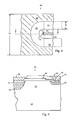
- FET 10 has a source electrode 12 in the shape of a line segment and a horse shoe-shaped drain electrode 14 that encircles one end of the source electrode 12. Electrode 12 has a diffusion 16 and electrode 14 has a diffusion 18 in a substrate 20. A polysilicon gate electrode 22 is insulated from the underlying silicon channel by a gate silicon oxide 24. In the prior art, such as FET 10, a channel comprising an n- drift region 26 uniformly surrounds both sides and the one end of the source 12. The width of the channel is roughly equal all around the source 12. The channel current could therefore be expected to be equally distributed. It has been observed that breakdown current flow occurs at the small radius tip of the source when a device is over-voltage stressed, e.g., a tip 28 in Fig. 1.
- n-well 18 radius near the gate will be about fifty microns with a drift 26 length of eighty microns for a 1,000 volt rated device.
- a first embodiment of the present invention is a field effect transistor (FET), presented in its lateral configuration, having, from a top view, a finger shaped source electrode surrounded by a horseshoe-shaped drain electrode.
- FET field effect transistor
- the traditional drain n-well and p-top which comprise the n- drift region, have been eliminated.
- a conventional channel area does exist in the areas between the source and drain where they are parallel to one another.
- a charge that unavoidably collects at the tip of the source has an electrically much wider source-drain gap, the FET therefore exhibits much higher breakdown voltages.
- the improved breakdown voltage characteristic is thus taken advantage of in this first embodiment by reducing the tip radius of the source and scaling down the overall size of the FET.
- An advantage of the present invention is that it provides semiconductor devices of higher breakdown voltages compared to similarly sized prior art devices.
- Another advantage of the present invention is that FETs with comparative breakdown voltages to those of the prior art can be made substantially smaller.
- Another advantage of the present invention is that the FET capacitances decrease as the device becomes smaller.
- FET 50 A field effect transistor (FET) 50, according to an embodiment of the present invention, is illustrated in Figs. 3 and 4.
- FET 50 is comprised of a source 52 having a tip 54, a gate 56, a drain 58, an area 60 lacking an n- drift diffusion, a pair of n- drift and p-top areas 62 on each lateral side of source 52, an n-well 64 associated with the drain 58, a p-well 66 for the source 52, and a p-type substrate 68.
- Source 52 comprises a metal in contact with an n + 70 and p- 72 in well 66.
- Drain 58 comprises a metal in contact with n + 74 in n-well 64.
- Gate 56 is comprised of polysilicon, and the insulating layers above and below it are comprised of silicon dioxide. Other materials common in the art may also be suitable.
- Tip 54 has a radius much smaller than tip 28 (Fig. 1). Therefore the overall geometry of FET 50 is much smaller than that of FET 10. Typically, tip 28 will have a radius of 50-75 microns, while tip 54 radius "r" is on the order of about ten microns.
- the outside width "w” of drain 58 can therefore be reduced two times the difference in radius "r". In this example, that would be, at a minimum, two times forty microns, for a total of an eighty micron reduction in FET 50. A typical resulting width "w” for a 1,000 volt FET would be 40%-50% smaller.
- the drift length "I” can be reduced to 65 microns from eighty microns.
- the "on" resistance (R on ) is improved with no degradation in breakdown voltage.
- FET 50 is merely an example for purposes of this discussion, and its size or layout should not be considered as limiting the present invention.
- FET 50 (Figs. 3 and 4), area 60 is unique. In the prior art it would comprise a normal channel cross-section, such as in Fig. 2. But in FET 50, the extension of n-well 64 beneath gate 56 has been reduced or eliminated and extends only under drain 58. The p-top of Fig. 2 is also absent from FET 50 in area 60. The vertical dotted line in Fig. 3 represents the boundary between area 60 and n-drift area 62. Above and below source 52, looking at it from Fig. 3, a "normal" channel area exists, in areas 62. As such, the normal channel areas will resemble that of Fig. 2.
- the difference between areas 60 and 62 is that, in area 60, a much higher voltage will be necessary to cause a breakdown between n-well 64 and p-well 66, compared to area 62.
- tip 54 has a very small radius "r" (e.g., ten microns) and the overall geometry of FET 50 is reduced.
- r e.g., ten microns
- the structure is such that any breakdown that does occur will happen in normal channel areas 62 where charge concentrations are minimum. The result of this is that FET 50 has both small overall geometry and a relatively high breakdown voltage characteristic.
- conductive features within semiconductor devices such as integrated circuits, that have sharp tips separated from other conductive layers by a dielectric, can have thicker dielectric insulation deposited in those areas proximate to the tips.
- the sharp end of an electrode normally in contact with a channel diffusion can be tipped in a dielectric.
- the present invention also embraces shaping a drain electrode to saddle a source electrode so that either end of the source electrode are away from the drain electrode.
- the channel exists therefore only inside the saddle, between the portions of the electrodes that are essentially parallel to one another.
- the shapes of the fingertips can be such that lateral electrical fields can sum within the plane of the surface, and if otherwise not compensated for, that will limit the breakdown voltage.
- fingertips are unavoidable.
- another embodiment of the present invention is a transistor having a source with one fingertip and a drain with two fingertips, one on either side of the source.
- the drain has a lightly doped drain diffusion (LDD) that is absent only around the source fingertip, leaving only substrate in that area.
- LDD lightly doped drain diffusion
Landscapes
- Insulated Gate Type Field-Effect Transistor (AREA)
Applications Claiming Priority (2)
| Application Number | Priority Date | Filing Date | Title |
|---|---|---|---|
| US808024 | 1991-12-12 | ||
| US07/808,024 US5258636A (en) | 1991-12-12 | 1991-12-12 | Narrow radius tips for high voltage semiconductor devices with interdigitated source and drain electrodes |
Publications (3)
| Publication Number | Publication Date |
|---|---|
| EP0546377A2 true EP0546377A2 (de) | 1993-06-16 |
| EP0546377A3 EP0546377A3 (en) | 1993-09-29 |
| EP0546377B1 EP0546377B1 (de) | 1998-03-11 |
Family
ID=25197683
Family Applications (1)
| Application Number | Title | Priority Date | Filing Date |
|---|---|---|---|
| EP92120030A Expired - Lifetime EP0546377B1 (de) | 1991-12-12 | 1992-11-25 | Halbleiteranordnung mit verbesserter Durchbruchspannungs-Charakteristik |
Country Status (4)
| Country | Link |
|---|---|
| US (1) | US5258636A (de) |
| EP (1) | EP0546377B1 (de) |
| JP (1) | JP2781504B2 (de) |
| DE (1) | DE69224709T2 (de) |
Cited By (5)
| Publication number | Priority date | Publication date | Assignee | Title |
|---|---|---|---|---|
| US5633521A (en) * | 1995-06-01 | 1997-05-27 | Nec Corporation | Enhancement of breakdown voltage in MOSFET semiconductor device |
| US6468866B2 (en) | 1995-10-30 | 2002-10-22 | Sgs-Thomson Microelectronics S.R.L. | Single feature size MOS technology power device |
| US6492691B2 (en) * | 1998-05-26 | 2002-12-10 | Stmicroelectronics S.R.L. | High integration density MOS technology power device structure |
| US6548864B2 (en) | 1995-10-30 | 2003-04-15 | Sgs Thomson Microelectronics | High density MOS technology power device |
| EP1089345A3 (de) * | 1999-09-28 | 2003-11-12 | Fuji Electric Co. Ltd. | Lateraler Leistungsfeldeffekttransistor |
Families Citing this family (70)
| Publication number | Priority date | Publication date | Assignee | Title |
|---|---|---|---|---|
| US5521105A (en) * | 1994-08-12 | 1996-05-28 | United Microelectronics Corporation | Method of forming counter-doped island in power MOSFET |
| DE69505348T2 (de) * | 1995-02-21 | 1999-03-11 | St Microelectronics Srl | Hochspannungs-MOSFET mit Feldplatten-Elektrode und Verfahren zur Herstellung |
| JP3228093B2 (ja) * | 1995-06-28 | 2001-11-12 | 富士電機株式会社 | 高耐圧ic |
| JP2755247B2 (ja) * | 1996-02-28 | 1998-05-20 | 日本電気株式会社 | 半導体装置 |
| US6207994B1 (en) * | 1996-11-05 | 2001-03-27 | Power Integrations, Inc. | High-voltage transistor with multi-layer conduction region |
| US6168983B1 (en) | 1996-11-05 | 2001-01-02 | Power Integrations, Inc. | Method of making a high-voltage transistor with multiple lateral conduction layers |
| US6639277B2 (en) | 1996-11-05 | 2003-10-28 | Power Integrations, Inc. | High-voltage transistor with multi-layer conduction region |
| TW400560B (en) * | 1996-12-23 | 2000-08-01 | Koninkl Philips Electronics Nv | Semiconductor device |
| DE19654113A1 (de) * | 1996-12-23 | 1998-06-25 | Asea Brown Boveri | Verfahren zum Herstellen eines MOS-gesteuerten Leistungshalbleiterbauelements |
| JP3142057B2 (ja) * | 1997-11-13 | 2001-03-07 | 日本電気株式会社 | 半導体装置とその製造方法、及び駆動装置 |
| US6084277A (en) * | 1999-02-18 | 2000-07-04 | Power Integrations, Inc. | Lateral power MOSFET with improved gate design |
| KR100360416B1 (ko) | 2000-04-12 | 2002-11-13 | 페어차일드코리아반도체 주식회사 | 높은 브레이크다운 전압을 갖는 전력용 반도체소자 및 그제조방법 |
| US6768171B2 (en) | 2000-11-27 | 2004-07-27 | Power Integrations, Inc. | High-voltage transistor with JFET conduction channels |
| US6509220B2 (en) | 2000-11-27 | 2003-01-21 | Power Integrations, Inc. | Method of fabricating a high-voltage transistor |
| US6424007B1 (en) | 2001-01-24 | 2002-07-23 | Power Integrations, Inc. | High-voltage transistor with buried conduction layer |
| US6773997B2 (en) * | 2001-07-31 | 2004-08-10 | Semiconductor Components Industries, L.L.C. | Method for manufacturing a high voltage MOSFET semiconductor device with enhanced charge controllability |
| US7221011B2 (en) * | 2001-09-07 | 2007-05-22 | Power Integrations, Inc. | High-voltage vertical transistor with a multi-gradient drain doping profile |
| US6573558B2 (en) * | 2001-09-07 | 2003-06-03 | Power Integrations, Inc. | High-voltage vertical transistor with a multi-layered extended drain structure |
| US6635544B2 (en) | 2001-09-07 | 2003-10-21 | Power Intergrations, Inc. | Method of fabricating a high-voltage transistor with a multi-layered extended drain structure |
| US6555873B2 (en) * | 2001-09-07 | 2003-04-29 | Power Integrations, Inc. | High-voltage lateral transistor with a multi-layered extended drain structure |
| US7786533B2 (en) * | 2001-09-07 | 2010-08-31 | Power Integrations, Inc. | High-voltage vertical transistor with edge termination structure |
| US6867100B2 (en) * | 2001-12-28 | 2005-03-15 | Texas Instruments Incorporated | System for high-precision double-diffused MOS transistors |
| US6730969B1 (en) * | 2002-06-27 | 2004-05-04 | National Semiconductor Corporation | Radiation hardened MOS transistor |
| DE10238797B4 (de) * | 2002-08-23 | 2007-09-20 | Infineon Technologies Ag | Kommutierfeste Diode und Verfahren zu ihrer Herstellung |
| US7026876B1 (en) | 2003-02-21 | 2006-04-11 | Dynalinear Technologies, Inc. | High linearity smart HBT power amplifiers for CDMA/WCDMA application |
| US6919598B2 (en) * | 2003-03-10 | 2005-07-19 | Zia Hossain | LDMOS transistor with enhanced termination region for high breakdown voltage with low on-resistance |
| US6982461B2 (en) * | 2003-12-08 | 2006-01-03 | Semiconductor Components Industries, L.L.C. | Lateral FET structure with improved blocking voltage and on resistance performance and method |
| US6903421B1 (en) | 2004-01-16 | 2005-06-07 | System General Corp. | Isolated high-voltage LDMOS transistor having a split well structure |
| JP4342498B2 (ja) * | 2005-09-30 | 2009-10-14 | パナソニック株式会社 | 横型半導体デバイス |
| US7829928B2 (en) * | 2006-06-26 | 2010-11-09 | System General Corp. | Semiconductor structure of a high side driver and method for manufacturing the same |
| US7759769B2 (en) * | 2006-07-20 | 2010-07-20 | System General Corp. | Semiconductor structure of a high side driver |
| US7589393B2 (en) * | 2006-07-25 | 2009-09-15 | System General Corporation | Semiconductor structure of a high side driver for two high voltage nodes with partially linked deep wells and method for manufacturing the same |
| US8093621B2 (en) | 2008-12-23 | 2012-01-10 | Power Integrations, Inc. | VTS insulated gate bipolar transistor |
| KR101371517B1 (ko) * | 2007-01-12 | 2014-03-12 | 페어차일드코리아반도체 주식회사 | 전계집중 감소용 플로팅영역을 구비한 고전압 반도체 소자 |
| US7859037B2 (en) * | 2007-02-16 | 2010-12-28 | Power Integrations, Inc. | Checkerboarded high-voltage vertical transistor layout |
| US7595523B2 (en) | 2007-02-16 | 2009-09-29 | Power Integrations, Inc. | Gate pullback at ends of high-voltage vertical transistor structure |
| US7557406B2 (en) | 2007-02-16 | 2009-07-07 | Power Integrations, Inc. | Segmented pillar layout for a high-voltage vertical transistor |
| US8653583B2 (en) | 2007-02-16 | 2014-02-18 | Power Integrations, Inc. | Sensing FET integrated with a high-voltage transistor |
| US7468536B2 (en) | 2007-02-16 | 2008-12-23 | Power Integrations, Inc. | Gate metal routing for transistor with checkerboarded layout |
| US7875962B2 (en) * | 2007-10-15 | 2011-01-25 | Power Integrations, Inc. | Package for a power semiconductor device |
| JP5150389B2 (ja) * | 2008-07-01 | 2013-02-20 | シャープ株式会社 | 半導体装置 |
| US7960786B2 (en) * | 2008-07-09 | 2011-06-14 | Taiwan Semiconductor Manufacturing Company, Ltd. | Breakdown voltages of ultra-high voltage devices by forming tunnels |
| US7964912B2 (en) | 2008-09-18 | 2011-06-21 | Power Integrations, Inc. | High-voltage vertical transistor with a varied width silicon pillar |
| US20100155831A1 (en) * | 2008-12-20 | 2010-06-24 | Power Integrations, Inc. | Deep trench insulated gate bipolar transistor |
| US7871882B2 (en) | 2008-12-20 | 2011-01-18 | Power Integrations, Inc. | Method of fabricating a deep trench insulated gate bipolar transistor |
| JP2010278312A (ja) * | 2009-05-29 | 2010-12-09 | Sanyo Electric Co Ltd | 半導体装置 |
| US8207455B2 (en) * | 2009-07-31 | 2012-06-26 | Power Integrations, Inc. | Power semiconductor package with bottom surface protrusions |
| US8115457B2 (en) | 2009-07-31 | 2012-02-14 | Power Integrations, Inc. | Method and apparatus for implementing a power converter input terminal voltage discharge circuit |
| US8207577B2 (en) * | 2009-09-29 | 2012-06-26 | Power Integrations, Inc. | High-voltage transistor structure with reduced gate capacitance |
| US7893754B1 (en) | 2009-10-02 | 2011-02-22 | Power Integrations, Inc. | Temperature independent reference circuit |
| US8634218B2 (en) * | 2009-10-06 | 2014-01-21 | Power Integrations, Inc. | Monolithic AC/DC converter for generating DC supply voltage |
| US8310845B2 (en) * | 2010-02-10 | 2012-11-13 | Power Integrations, Inc. | Power supply circuit with a control terminal for different functional modes of operation |
| JP5586546B2 (ja) * | 2011-03-23 | 2014-09-10 | 株式会社東芝 | 半導体装置 |
| WO2012158174A1 (en) * | 2011-05-19 | 2012-11-22 | Hewlett-Packard Development Company, L.P. | Device active channel length/width greater than channel length/width |
| TWI443832B (zh) | 2011-07-08 | 2014-07-01 | 新唐科技股份有限公司 | 金氧半場效電晶體 |
| US9269704B2 (en) * | 2012-05-15 | 2016-02-23 | Nuvoton Technology Corporation | Semiconductor device with embedded silicon-controlled rectifier |
| US8653600B2 (en) | 2012-06-01 | 2014-02-18 | Power Integrations, Inc. | High-voltage monolithic schottky device structure |
| TWI467766B (zh) | 2012-08-31 | 2015-01-01 | 新唐科技股份有限公司 | 金氧半場效電晶體及其製造方法 |
| CN103855208A (zh) * | 2012-11-28 | 2014-06-11 | 北大方正集团有限公司 | 一种高压ldmos集成器件 |
| CN103855210A (zh) * | 2012-12-03 | 2014-06-11 | 上海华虹宏力半导体制造有限公司 | 射频横向双扩散场效应晶体管及其制造方法 |
| US9660053B2 (en) | 2013-07-12 | 2017-05-23 | Power Integrations, Inc. | High-voltage field-effect transistor having multiple implanted layers |
| KR101941295B1 (ko) * | 2013-08-09 | 2019-01-23 | 매그나칩 반도체 유한회사 | 반도체 소자 |
| US9455621B2 (en) | 2013-08-28 | 2016-09-27 | Power Integrations, Inc. | Controller IC with zero-crossing detector and capacitor discharge switching element |
| US10325988B2 (en) | 2013-12-13 | 2019-06-18 | Power Integrations, Inc. | Vertical transistor device structure with cylindrically-shaped field plates |
| US9543396B2 (en) | 2013-12-13 | 2017-01-10 | Power Integrations, Inc. | Vertical transistor device structure with cylindrically-shaped regions |
| JP6388509B2 (ja) | 2014-08-19 | 2018-09-12 | ラピスセミコンダクタ株式会社 | 半導体装置および半導体装置の製造方法 |
| US9667154B2 (en) | 2015-09-18 | 2017-05-30 | Power Integrations, Inc. | Demand-controlled, low standby power linear shunt regulator |
| US9602009B1 (en) | 2015-12-08 | 2017-03-21 | Power Integrations, Inc. | Low voltage, closed loop controlled energy storage circuit |
| US9629218B1 (en) | 2015-12-28 | 2017-04-18 | Power Integrations, Inc. | Thermal protection for LED bleeder in fault condition |
| US12598799B2 (en) * | 2021-08-31 | 2026-04-07 | Texas Instruments Incorporated | High voltage finger layout transistor |
Family Cites Families (13)
| Publication number | Priority date | Publication date | Assignee | Title |
|---|---|---|---|---|
| JPS5638867A (en) * | 1979-09-07 | 1981-04-14 | Hitachi Ltd | Insulated gate type field effect transistor |
| DE3012185A1 (de) * | 1980-03-28 | 1981-10-08 | Siemens AG, 1000 Berlin und 8000 München | Feldeffekttransistor |
| JPS5712557A (en) * | 1980-06-25 | 1982-01-22 | Sanyo Electric Co Ltd | High dielectric resisting mos transistor |
| JPS5712558A (en) * | 1980-06-25 | 1982-01-22 | Sanyo Electric Co Ltd | Mos transistor having high withstand voltage |
| US4462041A (en) * | 1981-03-20 | 1984-07-24 | Harris Corporation | High speed and current gain insulated gate field effect transistors |
| JPS6064771A (ja) * | 1983-09-19 | 1985-04-13 | Daihen Corp | 溶接機制御装置 |
| US4894694A (en) * | 1986-10-31 | 1990-01-16 | Hewlett-Packard Company | MOSFET structure and method for making same |
| US4811075A (en) * | 1987-04-24 | 1989-03-07 | Power Integrations, Inc. | High voltage MOS transistors |
| US5025296A (en) * | 1988-02-29 | 1991-06-18 | Motorola, Inc. | Center tapped FET |
| JPH01264262A (ja) * | 1988-04-15 | 1989-10-20 | Toshiba Corp | Mos型電界効果トランジスタ |
| EP0371785B1 (de) * | 1988-11-29 | 1996-05-01 | Kabushiki Kaisha Toshiba | Lateraler Leitfähigkeitsmodulations-MOSFET |
| US5055896A (en) * | 1988-12-15 | 1991-10-08 | Siliconix Incorporated | Self-aligned LDD lateral DMOS transistor with high-voltage interconnect capability |
| US5040045A (en) * | 1990-05-17 | 1991-08-13 | U.S. Philips Corporation | High voltage MOS transistor having shielded crossover path for a high voltage connection bus |
-
1991
- 1991-12-12 US US07/808,024 patent/US5258636A/en not_active Expired - Lifetime
-
1992
- 1992-11-25 DE DE69224709T patent/DE69224709T2/de not_active Expired - Lifetime
- 1992-11-25 EP EP92120030A patent/EP0546377B1/de not_active Expired - Lifetime
- 1992-12-11 JP JP4331898A patent/JP2781504B2/ja not_active Expired - Lifetime
Cited By (6)
| Publication number | Priority date | Publication date | Assignee | Title |
|---|---|---|---|---|
| US5633521A (en) * | 1995-06-01 | 1997-05-27 | Nec Corporation | Enhancement of breakdown voltage in MOSFET semiconductor device |
| US6468866B2 (en) | 1995-10-30 | 2002-10-22 | Sgs-Thomson Microelectronics S.R.L. | Single feature size MOS technology power device |
| US6548864B2 (en) | 1995-10-30 | 2003-04-15 | Sgs Thomson Microelectronics | High density MOS technology power device |
| US6566690B2 (en) | 1995-10-30 | 2003-05-20 | Sgs Thomson Microelectronics S.R.L. | Single feature size MOS technology power device |
| US6492691B2 (en) * | 1998-05-26 | 2002-12-10 | Stmicroelectronics S.R.L. | High integration density MOS technology power device structure |
| EP1089345A3 (de) * | 1999-09-28 | 2003-11-12 | Fuji Electric Co. Ltd. | Lateraler Leistungsfeldeffekttransistor |
Also Published As
| Publication number | Publication date |
|---|---|
| EP0546377A3 (en) | 1993-09-29 |
| US5258636A (en) | 1993-11-02 |
| EP0546377B1 (de) | 1998-03-11 |
| DE69224709T2 (de) | 1998-10-29 |
| JP2781504B2 (ja) | 1998-07-30 |
| DE69224709D1 (de) | 1998-04-16 |
| JPH05259454A (ja) | 1993-10-08 |
Similar Documents
| Publication | Publication Date | Title |
|---|---|---|
| US5258636A (en) | Narrow radius tips for high voltage semiconductor devices with interdigitated source and drain electrodes | |
| KR100649328B1 (ko) | 고전압 금속 산화막 반도체 전계 효과 트랜지스터 구조 | |
| US5710455A (en) | Lateral MOSFET with modified field plates and damage areas | |
| US6630698B1 (en) | High-voltage semiconductor component | |
| KR100652449B1 (ko) | 횡형 박막 실리콘-온-절연체 jfet 디바이스 | |
| US7777278B2 (en) | Lateral semiconductor component with a drift zone having at least one field electrode | |
| EP0788660B1 (de) | Halbleiteranordnung vom hochspannungs-ldmos-typ | |
| US8536641B1 (en) | Semiconductor device | |
| US6110804A (en) | Method of fabricating a semiconductor device having a floating field conductor | |
| US5569937A (en) | High breakdown voltage silicon carbide transistor | |
| US6888210B2 (en) | Lateral DMOS transistor having reduced surface field | |
| US20200295150A1 (en) | Semiconductor device | |
| US20230010328A1 (en) | Shielded gate trench mosfet with multiple stepped epitaxial structures | |
| EP0809864B1 (de) | Laterale dünnfilm-soi-anordnungen mit einem gradierten feldoxid und linearem dopierungsprofil | |
| US9735263B2 (en) | Transistor and switching system comprising silicon carbide and oxides of varying thicknesses, and method for providing the same | |
| JP3218267B2 (ja) | 半導体装置 | |
| US6930356B2 (en) | Power semiconductor device having high breakdown voltage, low on-resistance, and small switching loss and method of forming the same | |
| US6982461B2 (en) | Lateral FET structure with improved blocking voltage and on resistance performance and method | |
| US20020130361A1 (en) | Semiconductor device with laterally varying p-top layers | |
| EP0802567A3 (de) | Halbleiteranordnung und Verfahren zu ihrer Herstellung | |
| US10460931B2 (en) | Semiconductor transistor having superlattice structures | |
| US20230352520A1 (en) | Wide band gap semiconductor device | |
| US20230307535A1 (en) | Semiconductor device | |
| US20070075367A1 (en) | SOI semiconductor component with increased dielectric strength | |
| EP4432363A1 (de) | Halbleiteranordnung |
Legal Events
| Date | Code | Title | Description |
|---|---|---|---|
| PUAI | Public reference made under article 153(3) epc to a published international application that has entered the european phase |
Free format text: ORIGINAL CODE: 0009012 |
|
| AK | Designated contracting states |
Kind code of ref document: A2 Designated state(s): DE FR GB IT NL SE |
|
| PUAL | Search report despatched |
Free format text: ORIGINAL CODE: 0009013 |
|
| AK | Designated contracting states |
Kind code of ref document: A3 Designated state(s): DE FR GB IT NL SE |
|
| 17P | Request for examination filed |
Effective date: 19940316 |
|
| 17Q | First examination report despatched |
Effective date: 19950530 |
|
| GRAG | Despatch of communication of intention to grant |
Free format text: ORIGINAL CODE: EPIDOS AGRA |
|
| GRAG | Despatch of communication of intention to grant |
Free format text: ORIGINAL CODE: EPIDOS AGRA |
|
| GRAH | Despatch of communication of intention to grant a patent |
Free format text: ORIGINAL CODE: EPIDOS IGRA |
|
| GRAH | Despatch of communication of intention to grant a patent |
Free format text: ORIGINAL CODE: EPIDOS IGRA |
|
| ITF | It: translation for a ep patent filed | ||
| GRAA | (expected) grant |
Free format text: ORIGINAL CODE: 0009210 |
|
| AK | Designated contracting states |
Kind code of ref document: B1 Designated state(s): DE FR GB IT NL SE |
|
| REF | Corresponds to: |
Ref document number: 69224709 Country of ref document: DE Date of ref document: 19980416 |
|
| ET | Fr: translation filed | ||
| PLBE | No opposition filed within time limit |
Free format text: ORIGINAL CODE: 0009261 |
|
| STAA | Information on the status of an ep patent application or granted ep patent |
Free format text: STATUS: NO OPPOSITION FILED WITHIN TIME LIMIT |
|
| 26N | No opposition filed | ||
| REG | Reference to a national code |
Ref country code: GB Ref legal event code: IF02 |
|
| PGFP | Annual fee paid to national office [announced via postgrant information from national office to epo] |
Ref country code: DE Payment date: 20101126 Year of fee payment: 19 |
|
| PGFP | Annual fee paid to national office [announced via postgrant information from national office to epo] |
Ref country code: IT Payment date: 20101124 Year of fee payment: 19 Ref country code: GB Payment date: 20101124 Year of fee payment: 19 |
|
| PGFP | Annual fee paid to national office [announced via postgrant information from national office to epo] |
Ref country code: NL Payment date: 20111129 Year of fee payment: 20 Ref country code: SE Payment date: 20111125 Year of fee payment: 20 Ref country code: FR Payment date: 20111128 Year of fee payment: 20 |
|
| REG | Reference to a national code |
Ref country code: DE Ref legal event code: R071 Ref document number: 69224709 Country of ref document: DE |
|
| REG | Reference to a national code |
Ref country code: NL Ref legal event code: V4 Effective date: 20121125 |
|
| REG | Reference to a national code |
Ref country code: GB Ref legal event code: PE20 Expiry date: 20121124 |
|
| REG | Reference to a national code |
Ref country code: SE Ref legal event code: EUG |
|
| PG25 | Lapsed in a contracting state [announced via postgrant information from national office to epo] |
Ref country code: GB Free format text: LAPSE BECAUSE OF EXPIRATION OF PROTECTION Effective date: 20121124 |