EP0458407A2 - Abtastung einer analogen Signalspannung - Google Patents
Abtastung einer analogen Signalspannung Download PDFInfo
- Publication number
- EP0458407A2 EP0458407A2 EP91201192A EP91201192A EP0458407A2 EP 0458407 A2 EP0458407 A2 EP 0458407A2 EP 91201192 A EP91201192 A EP 91201192A EP 91201192 A EP91201192 A EP 91201192A EP 0458407 A2 EP0458407 A2 EP 0458407A2
- Authority
- EP
- European Patent Office
- Prior art keywords
- gate electrode
- potential
- barrier
- well
- source region
- Prior art date
- Legal status (The legal status is an assumption and is not a legal conclusion. Google has not performed a legal analysis and makes no representation as to the accuracy of the status listed.)
- Withdrawn
Links
- 238000005070 sampling Methods 0.000 title claims description 11
- 238000005036 potential barrier Methods 0.000 claims abstract description 62
- 239000002800 charge carrier Substances 0.000 claims abstract description 39
- 238000000034 method Methods 0.000 claims abstract description 17
- 239000004065 semiconductor Substances 0.000 claims abstract description 9
- 239000000969 carrier Substances 0.000 claims abstract description 7
- 230000004888 barrier function Effects 0.000 claims description 32
- 239000000758 substrate Substances 0.000 claims description 18
- 230000000630 rising effect Effects 0.000 abstract description 2
- 108091006146 Channels Proteins 0.000 description 18
- 238000009792 diffusion process Methods 0.000 description 4
- 230000007704 transition Effects 0.000 description 4
- 239000000463 material Substances 0.000 description 3
- 230000000694 effects Effects 0.000 description 2
- 238000005516 engineering process Methods 0.000 description 2
- 238000012986 modification Methods 0.000 description 2
- 230000004048 modification Effects 0.000 description 2
- 108090000699 N-Type Calcium Channels Proteins 0.000 description 1
- 108010075750 P-Type Calcium Channels Proteins 0.000 description 1
- 230000009286 beneficial effect Effects 0.000 description 1
- 230000008901 benefit Effects 0.000 description 1
- 238000010276 construction Methods 0.000 description 1
- 238000004519 manufacturing process Methods 0.000 description 1
- 230000037230 mobility Effects 0.000 description 1
- 229910021420 polycrystalline silicon Inorganic materials 0.000 description 1
- 229920005591 polysilicon Polymers 0.000 description 1
- 230000004044 response Effects 0.000 description 1
- 229910052710 silicon Inorganic materials 0.000 description 1
- 239000010703 silicon Substances 0.000 description 1
Images

Classifications
-
- G—PHYSICS
- G11—INFORMATION STORAGE
- G11C—STATIC STORES
- G11C27/00—Electric analogue stores, e.g. for storing instantaneous values
- G11C27/04—Shift registers
Definitions
- One aspect of this invention relates to apparatus for sampling an analogue signal voltage to provide charge packets the sizes of which are representative of successive samples, said apparatus comprising a semiconductor substrate of a given conductivity type within and adjacent a surface of which a charge carrier source region of the opposite conductivity type is provided and a channel region for transporting charge carriers from said source region is defined, said channel region having the given or the opposite conductivity type and having a plurality of gate electrodes insulatingly overlying it for controlling the charge carrier transport, said electrodes including a first gate electrode for forming a metering potential well within said channel region, a second gate electrode for forming a first potential barrier within said channel region between said metering potential well and said source region, and a third gate electrode for controlling the transfer of charge packets from said metering potential well towards an output, said apparatus furthermore comprising an input for said analogue signal voltage, which input is coupled to said first gate electrode, and a control signal generator arrangement coupled to said second region and to said first, second and third gate electrodes for applying a
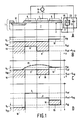
- the potential of the region 10 is more positive than the potential V ref of the top of the first potential barrier 9, so that barrier 9 acts to prevent electrons from entering the metering well 8 from the region 10 at this time.
- FIG. 2 corresponding items have been given the same reference numerals as their counterparts in Figure 1.
- the embodiment of the invention shown in Figure 2A differs from the known apparatus shown in Figure 1A in that a comparatively short (in the direction from electrode to electrode) fourth electrode 20 is provided on the insulating layer 3 between the electrode 5 and the electrode 4, and clock pulse generator 11 is provided with a second input 19 which is connected to electrode 20.
- the clock pulses produced at output 19 are in antiphase to those produced at output 18 and the resulting voltages on electrode 20 cause a third potential barrier to be created in the part of region 7 under electrode 20, i.e. between the first potential barrier created under electrode 5 and the metering potential well created under electrode 4.
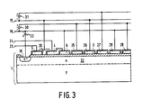
- the electrode 6 (c.f. Figure 2A) together with an electrode 25 forms the first half of the first transfer cell of the device, and electrodes 26 and 27 form the second half. Similarly electrodes 28 and 29 form the first half of the second transfer cell.
- the first electrode of the first half of each transfer cell is connected to the output 18 of the clock pulse generator 11 of Figure 2 and the second electrode of the first half of each transfer cell is connected to the output 18 via a voltage source 30.
- the first electrode of the second half of each transfer cell is connected to the output 19 of the clock pulse generator 11 of Figure 2 and the second electrode of the second half of each transfer cell is connected to the output 19 via a voltage source 31.
Landscapes
- Solid State Image Pick-Up Elements (AREA)
- Analogue/Digital Conversion (AREA)
Applications Claiming Priority (2)
| Application Number | Priority Date | Filing Date | Title |
|---|---|---|---|
| GB9011507A GB2244399A (en) | 1990-05-23 | 1990-05-23 | Sampling analogue signals |
| GB9011507 | 1990-05-25 |
Publications (2)
| Publication Number | Publication Date |
|---|---|
| EP0458407A2 true EP0458407A2 (de) | 1991-11-27 |
| EP0458407A3 EP0458407A3 (en) | 1992-09-09 |
Family
ID=10676408
Family Applications (1)
| Application Number | Title | Priority Date | Filing Date |
|---|---|---|---|
| EP19910201192 Withdrawn EP0458407A3 (en) | 1990-05-23 | 1991-05-17 | Sampling an analogue signal voltage |
Country Status (4)
| Country | Link |
|---|---|
| US (1) | US5146480A (de) |
| EP (1) | EP0458407A3 (de) |
| JP (1) | JPH04229630A (de) |
| GB (1) | GB2244399A (de) |
Families Citing this family (4)
| Publication number | Priority date | Publication date | Assignee | Title |
|---|---|---|---|---|
| US6847070B2 (en) * | 2000-08-09 | 2005-01-25 | Dalsa, Inc. | Five transistor CMOS pixel |
| US7045753B1 (en) | 2000-08-09 | 2006-05-16 | Dalsa, Inc. | Five transistor CMOS pixel |
| US6566697B1 (en) | 2000-11-28 | 2003-05-20 | Dalsa, Inc. | Pinned photodiode five transistor pixel |
| US20090122173A1 (en) * | 2007-11-13 | 2009-05-14 | William Emerson Tennant | Low noise readout apparatus and method for cmos image sensors |
Family Cites Families (6)
| Publication number | Priority date | Publication date | Assignee | Title |
|---|---|---|---|---|
| CA983618A (en) * | 1973-04-23 | 1976-02-10 | Robert J. Strain | Analog inverter for use in charge transfer apparatus |
| US3986198A (en) * | 1973-06-13 | 1976-10-12 | Rca Corporation | Introducing signal at low noise level to charge-coupled circuit |
| DE2541510A1 (de) * | 1974-09-17 | 1976-03-25 | Westinghouse Electric Corp | Verarbeitungssystem fuer diskrete analogsignale |
| US4178519A (en) * | 1978-08-16 | 1979-12-11 | General Electric Company | Input circuit for charge transfer apparatus |
| DE2836473A1 (de) * | 1978-08-21 | 1980-03-06 | Siemens Ag | Ccd-eingangsschaltung nach dem fill and spill-prinzip |
| JPH0728029B2 (ja) * | 1987-05-21 | 1995-03-29 | 株式会社東芝 | 電荷転送素子 |
-
1990
- 1990-05-23 GB GB9011507A patent/GB2244399A/en not_active Withdrawn
-
1991
- 1991-04-19 US US07/688,015 patent/US5146480A/en not_active Expired - Fee Related
- 1991-05-17 EP EP19910201192 patent/EP0458407A3/en not_active Withdrawn
- 1991-05-21 JP JP3144155A patent/JPH04229630A/ja active Pending
Non-Patent Citations (2)
| Title |
|---|
| PROCEEDINGS OF THE IEEE 1986 CUSTOM INTEGRATED CIRCUITS CONFERENCE 15 May 1986, NEW YORK, USA pages 521 - 527; SAHAI ET AL.: 'GaAs CCDs for analog signal processing ICs' * |
| TRANSACTIONS OF THE INSTITUTE OF ELECTRONICS AND COMMUNICATION vol. E63, no. 7, July 1980, TOKYO JP pages 530 - 531; YONEI: 'Linearity of Dynamic Injection into CCD with Resistive Input Gate' * |
Also Published As
| Publication number | Publication date |
|---|---|
| GB2244399A (en) | 1991-11-27 |
| JPH04229630A (ja) | 1992-08-19 |
| EP0458407A3 (en) | 1992-09-09 |
| GB9011507D0 (en) | 1990-07-11 |
| US5146480A (en) | 1992-09-08 |
Similar Documents
| Publication | Publication Date | Title |
|---|---|---|
| Tompsett | Surface potential equilibration method of setting charge in charge-coupled devices | |
| CA1120588A (en) | Ccd input circuits | |
| US4112456A (en) | Stabilized charge injector for charge coupled devices with means for increasing the speed of propagation of charge carriers | |
| US4012759A (en) | Bulk channel charge transfer device | |
| CA1089986A (en) | Operating circuitry for semiconductor charge coupled devices | |
| US4136335A (en) | Semiconductor charge coupled device analog to digital converter | |
| US4727560A (en) | Charge-coupled device with reduced signal distortion | |
| US4040077A (en) | Time-independent ccd charge amplifier | |
| US5146480A (en) | Sampling an analog signal voltage using fill and spill input in charge transfer device | |
| Krambeck et al. | A Doped Surface Two‐Phase CCD | |
| US3935477A (en) | Analog inverter for use in charge transfer apparatus | |
| US4594604A (en) | Charge coupled device with structures for forward scuppering to reduce noise | |
| CA1101994A (en) | Linear ccd input circuit | |
| US4321584A (en) | Charge coupled digital-to-analog converter | |
| US4891826A (en) | Method of operating a charge-coupled device to reduce spillback | |
| US3918081A (en) | Integrated semiconductor device employing charge storage and charge transport for memory or delay line | |
| US5132656A (en) | Floating-gate charge-balance ccd | |
| US7880782B2 (en) | Image sensor clocking method | |
| US4277694A (en) | Charge coupled device variable divider with integrating well | |
| US4194133A (en) | Charge coupled circuit arrangements and devices having controlled punch-through charge introduction | |
| McKenna et al. | Design Considerations for a Two‐Phase, Buried‐Channel, Charge‐Coupled Device | |
| Arora | Charge coupled devices—Basic operation and principles | |
| Kwon et al. | Characteristics of band modulation FET on sub 10 nm SOI | |
| Haken | Supply charge isolation-a simple surface potential equilibration charge-injection technique for charge-coupled devices | |
| GB2025135A (en) | A bulk-channel charge coupled device |
Legal Events
| Date | Code | Title | Description |
|---|---|---|---|
| PUAI | Public reference made under article 153(3) epc to a published international application that has entered the european phase |
Free format text: ORIGINAL CODE: 0009012 |
|
| AK | Designated contracting states |
Kind code of ref document: A2 Designated state(s): DE FR GB IT NL |
|
| PUAL | Search report despatched |
Free format text: ORIGINAL CODE: 0009013 |
|
| AK | Designated contracting states |
Kind code of ref document: A3 Designated state(s): DE FR GB IT NL |
|
| 17P | Request for examination filed |
Effective date: 19930305 |
|
| STAA | Information on the status of an ep patent application or granted ep patent |
Free format text: STATUS: THE APPLICATION HAS BEEN WITHDRAWN |
|
| 18W | Application withdrawn |
Withdrawal date: 19950109 |