EP0458958B1 - Tete d'impression a jet de bulles a structure d'actionnement multiplex amelioree - Google Patents
Tete d'impression a jet de bulles a structure d'actionnement multiplex amelioree Download PDFInfo
- Publication number
- EP0458958B1 EP0458958B1 EP91902342A EP91902342A EP0458958B1 EP 0458958 B1 EP0458958 B1 EP 0458958B1 EP 91902342 A EP91902342 A EP 91902342A EP 91902342 A EP91902342 A EP 91902342A EP 0458958 B1 EP0458958 B1 EP 0458958B1
- Authority
- EP
- European Patent Office
- Prior art keywords
- circuit
- circuit portion
- passivation layer
- branches
- overlying
- Prior art date
- Legal status (The legal status is an assumption and is not a legal conclusion. Google has not performed a legal analysis and makes no representation as to the accuracy of the status listed.)
- Expired - Lifetime
Links
- 238000010276 construction Methods 0.000 title abstract description 16
- 238000002161 passivation Methods 0.000 claims abstract description 21
- 239000000758 substrate Substances 0.000 claims abstract description 16
- 230000008878 coupling Effects 0.000 claims description 7
- 238000010168 coupling process Methods 0.000 claims description 7
- 238000005859 coupling reaction Methods 0.000 claims description 7
- 239000010409 thin film Substances 0.000 claims description 3
- VYPSYNLAJGMNEJ-UHFFFAOYSA-N Silicium dioxide Chemical compound O=[Si]=O VYPSYNLAJGMNEJ-UHFFFAOYSA-N 0.000 description 6
- 238000013459 approach Methods 0.000 description 6
- 238000003491 array Methods 0.000 description 5
- 238000010438 heat treatment Methods 0.000 description 5
- 239000000463 material Substances 0.000 description 5
- 238000007639 printing Methods 0.000 description 5
- 239000002184 metal Substances 0.000 description 4
- 229910052751 metal Inorganic materials 0.000 description 4
- XUIMIQQOPSSXEZ-UHFFFAOYSA-N Silicon Chemical compound [Si] XUIMIQQOPSSXEZ-UHFFFAOYSA-N 0.000 description 3
- 230000015572 biosynthetic process Effects 0.000 description 3
- 229910052681 coesite Inorganic materials 0.000 description 3
- 229910052906 cristobalite Inorganic materials 0.000 description 3
- 230000000694 effects Effects 0.000 description 3
- 238000004519 manufacturing process Methods 0.000 description 3
- 239000011159 matrix material Substances 0.000 description 3
- 229910052710 silicon Inorganic materials 0.000 description 3
- 239000010703 silicon Substances 0.000 description 3
- 239000000377 silicon dioxide Substances 0.000 description 3
- 235000012239 silicon dioxide Nutrition 0.000 description 3
- 229910052682 stishovite Inorganic materials 0.000 description 3
- 229910052905 tridymite Inorganic materials 0.000 description 3
- 239000004952 Polyamide Substances 0.000 description 2
- MCMNRKCIXSYSNV-UHFFFAOYSA-N Zirconium dioxide Chemical compound O=[Zr]=O MCMNRKCIXSYSNV-UHFFFAOYSA-N 0.000 description 2
- 229920002647 polyamide Polymers 0.000 description 2
- 238000012546 transfer Methods 0.000 description 2
- 229910003862 HfB2 Inorganic materials 0.000 description 1
- 239000000853 adhesive Substances 0.000 description 1
- 230000001070 adhesive effect Effects 0.000 description 1
- 239000011248 coating agent Substances 0.000 description 1
- 238000000576 coating method Methods 0.000 description 1
- 239000004020 conductor Substances 0.000 description 1
- 238000011161 development Methods 0.000 description 1
- 238000005516 engineering process Methods 0.000 description 1
- 238000001914 filtration Methods 0.000 description 1
- 239000011521 glass Substances 0.000 description 1
- PCHJSUWPFVWCPO-UHFFFAOYSA-N gold Chemical compound [Au] PCHJSUWPFVWCPO-UHFFFAOYSA-N 0.000 description 1
- 239000010931 gold Substances 0.000 description 1
- 229910052737 gold Inorganic materials 0.000 description 1
- 230000020169 heat generation Effects 0.000 description 1
- 238000000034 method Methods 0.000 description 1
- 238000012986 modification Methods 0.000 description 1
- 230000004048 modification Effects 0.000 description 1
- 238000013021 overheating Methods 0.000 description 1
- 238000000059 patterning Methods 0.000 description 1
- 239000011253 protective coating Substances 0.000 description 1
- 230000001681 protective effect Effects 0.000 description 1
- 239000004065 semiconductor Substances 0.000 description 1
- 230000035939 shock Effects 0.000 description 1
- 238000012876 topography Methods 0.000 description 1
Images


Classifications
-
- B—PERFORMING OPERATIONS; TRANSPORTING
- B41—PRINTING; LINING MACHINES; TYPEWRITERS; STAMPS
- B41J—TYPEWRITERS; SELECTIVE PRINTING MECHANISMS, i.e. MECHANISMS PRINTING OTHERWISE THAN FROM A FORME; CORRECTION OF TYPOGRAPHICAL ERRORS
- B41J2/00—Typewriters or selective printing mechanisms characterised by the printing or marking process for which they are designed
- B41J2/005—Typewriters or selective printing mechanisms characterised by the printing or marking process for which they are designed characterised by bringing liquid or particles selectively into contact with a printing material
- B41J2/01—Ink jet
- B41J2/135—Nozzles
- B41J2/14—Structure thereof only for on-demand ink jet heads
- B41J2/14016—Structure of bubble jet print heads
- B41J2/14088—Structure of heating means
- B41J2/14112—Resistive element
- B41J2/14129—Layer structure
-
- B—PERFORMING OPERATIONS; TRANSPORTING
- B41—PRINTING; LINING MACHINES; TYPEWRITERS; STAMPS
- B41J—TYPEWRITERS; SELECTIVE PRINTING MECHANISMS, i.e. MECHANISMS PRINTING OTHERWISE THAN FROM A FORME; CORRECTION OF TYPOGRAPHICAL ERRORS
- B41J2/00—Typewriters or selective printing mechanisms characterised by the printing or marking process for which they are designed
- B41J2/005—Typewriters or selective printing mechanisms characterised by the printing or marking process for which they are designed characterised by bringing liquid or particles selectively into contact with a printing material
- B41J2/01—Ink jet
- B41J2/135—Nozzles
- B41J2/14—Structure thereof only for on-demand ink jet heads
- B41J2/14016—Structure of bubble jet print heads
- B41J2/14072—Electrical connections, e.g. details on electrodes, connecting the chip to the outside...
Definitions
- the present invention relates to thermal, drop-on-demand, ink jet (herein termed "bubble jet”) printing and, more particularly, to improved print head constructions for enabling high density printing.
- bubble jet thermal, drop-on-demand, ink jet
- a plurality of electrically resistive heater elements are deposited on a support substrate that is formed e.g. of metal or silicon and has a heat control coating, e.g. SiO2.
- Metal electrodes are formed to selectively apply voltage across the heater elements and a protective coating is provided over the heater elements and electrodes.
- Printing ink is supplied between the heater elements and orifices of the print head and heater elements are selectively energized to a temperature that converts the adjacent ink to steam rapidly, so that a shock wave causes ejection of ink from the related orifice.
- system resolution can be thought of as the number of pixel drops printed within a given print region (e.g. line length).
- One way to increase system resolution is to interlace ink drops, e.g. with multiple passes vis a vis a single array of orifices, or by providing a plurality of scanning orifice arrays. This approach simplifies the print head(s) construction, but requires accurate positioning of the print heads vis a vis the print media to assure good registration of the drops from separate passes.
- Another way to increase system resolution is to increase the line density of drop ejector subsystems (i.e. orifices and related heater elements) on a single print head. This can be done with one or a plurality of linear orifice arrays (see e.g. U.S. Patent No. 4,734,717).
- Photofabrication techniques enable construction of such high density orifice plate and heater subsystems; however, a present limit to increasing system resolution is presented by the difficulty in making electrical connections between a large number of heating resistors formed on a tiny chip and the electrical address electronics of the printer control system.
- U.S. Patent 4,695,853 discloses a bubble jet chip construction wherein an x-y electrode matrix is constructed with one matrix electrode portion underlying a pattern of resistor/diodes and the other matrix electrode portion overlying the resistor/diode pattern.
- the x-y electrode portions are separated by an electrically insulative layer except at the resistor/diode components where they form "vertically" disposed, sandwiching terminals.
- U.S. Patent 4,791,440 discloses another solution to the problem of providing a high resolution print head with a large number of drop-ejection sites.
- one array of electrical connections to the sites is provided on the top side of the chip substrate and another array of site connections is provided on the bottom side of the substrate.
- a plurality of holes are provided through the substrate material to couple the top and bottom side lead matrices.
- this approach provides also a multiplex address system wherein a plurality of heater arrays are activated at different phases by an array-select voltage pulse, which, when coupled with a particular heat site data pulse, will provide sufficient heater current to eject an ink drop.
- the '440 patent approach is a difficult one to fabricate, necessitating the forming of multiple holes though the substrate and photofabrication work on both sides of the substrate. In some applications coupling to the printer via the chip bottom surface is not possible. Also, the multiplex system causes unnecessary partial energizations of all heater elements during each active phase of an array. This can cause dissolved gas release from the ink resulting in a bubble which blocks jet activity or ink replenishment.
- a significant purpose of the present invention is to provide an improved construction for a high resolution bubble jet print head which avoids the problems of prior art approaches such as described above.
- one advantage of the present invention is to enable relatively simple fabrication of a bubble jet print head having a large number of high density drop ejection sites.
- Another advantage of the present invention is provision of a multiplex print head construction that operates more reliably and efficiently than prior art approaches.
- the life of a bubble jet heater array resistor is a very strong function of the voltage at which it is operated. Thus, it is desirable to operate such elements as close to the bubble formation threshold as possible. They may have, for example, a life of only a few cycles at 25% above threshold, but a life of several million cycles at 10% above threshold. Since there are manufacturing tolerances in the supply voltage, various lead resistances, and the threshold voltage, and the desire is to extract excellent life (by operating close to the bubble formation threshold) all resistance variations should be held to a minimum. Because semiconductor diodes in contrast to ordinary conductors decrease their forward resistance as they increase in temperature, the use of diodes in an ink heating region creates great potential for overall circuit resistance variation, if not thermal runaway. Thus, use of resistor/diodes, as in the '853 patent, is not desirable from the viewpoint of a long device operating life.
- the present invention provides an improved construction for a drop-on-demand, ink jet printer of the kind having a plurality of orifices, a thin film drop ejector, including heater elements, and manifold means for supplying ink to the heater elements.
- the improved construction constitutes a drop ejection device having (i) a support substrate; (ii) a first circuit comprising a plurality of circuit branches that each include a resistive heater element and a diode device, formed in spaced relation on the substrate; (iii) a dielectric passivation layer overlying the first circuit except at the discrete terminal regions; (iv) a second circuit comprising a plurality of multiplex electrode lines overlying the passivation layer and including connection sections extending through the passivation layer into contact with terminal regions of the first circuit; and (v) a second passivation layer overlying the second circuit portion but not overlying the resistive heater elements.
- FIG. 1 illustrates one bubble jet print/cartridge embodiment of the present invention, which is a modification of the print/cartridge described in U.S. Patent No. 4,734,717.
- the print/cartridge 10 comprises an ink reservoir portion 11 having a cap 12 with filtering ink supply openings 13 that lead via supply passages 14 to manifold regions 15.
- a drop ejection chip 16 mounts over the top of the cap and has openings 17 aligned with manifold region 15.
- An orifice plate 18 having two linear arrays of orifices 18a, 18b is mounted, by a printed adhesive pattern 19, over the top of openings 17 and the resistive heater elements formed in corresponding arrays 20a, 20b on the top surface of the drop ejection chip. As shown generally in FIG.
- the chip 16 also has group address electrodes 22a, 22b and group selection electrodes 23, 24.
- a significant aspect of the present invention is the improved construction and function of the chip 16 and its circuits, which are described in detail subsequently.
- ink is supplied, e.g. by capillary action, from the ink reservoir to regions over the resistive heater elements.
- Current pulses are selectively directed via chip electrodes, through the heater elements, in accord with information signals that gate driver circuits (not shown). The current pulses heat the resistive elements, which vaporize adjacent ink to eject drops of ink from the related orifices.
- the circuit system comprises a first circuit portion, which is formed on a substrate and is indicated by solid lines, second circuit portions (indicated by stippled regions) and a dielectric passivation layer (not shown) intermediate the two circuit portions.
- the first circuit portion comprises a plurality of branch subcircuits 31a-31L that each include a resistive heater element 32 and a diode 33 formed in spaced relation on the substrate and coupled by electrode lines 35 (see subcircuit 31g).
- Branch electrode lines for subcircuits 31a-31c and 31g-31i extend directly to terminals 36-A, 36-B which are connectible to print pulse drive circuits (not shown).
- the second circuit portion comprises six coupling electrode portions 37, which connect the input terminals 36-A, 36-B to respective lines of subcircuits 31c-31d and 31j-31L, and two group selection electrodes 38, 39 which are coupled respectively to the opposite ends of subcircuit lines to form subcircuit selection group I (31a-31c and 31g-31i) and group II (31d-31f and 31j-31L).
- Selection electrode 38 extends to a group I selection terminal 40 and selection electrode 39 extends to group II selection terminal 41.
- the cross-hatched areas on the stippled second circuit indicate regions where the electrode extends through the intermediate dielectric passivation layer to make contact with the first circuit portion branches. Otherwise the two circuit portions are electrically isolated from one another by the dielectric passivation layer.
- FIG. 3 shown a cross-section of a portion of one actual circuit structure, such as illustrated schematically within the dotted line box 50 of FIG. 2.
- substrate 51 can comprise a glass or glazed silicon chip having a heat control top surface (not shown) on which a resistive metal layer 32 (e.g. TaA1 or HfB2) is formed.
- Electrode leads 35a, 35b are deposited onto the resistive layer except over the ink heating region H so that current will pass from one electrode to another, down through the resistive layer at the heating region.
- First passivation layer 52 e.g. SiO2, is formed over the electrodes and heater elements except at regions 53, 54.
- a coupling portion of electrode 37 extends into contact with address electrode 35a and over the surface of the dielectric passivation layer 52 to couple with branch circuit 31d (not shown in FIG. 3).
- a diode layer (e.g. comprising silicon and gold) is first deposited and then a coupling portion of group select electrode 38 is deposited to extend over layer 52 to terminal 40 (not shown in FIG. 3).
- a second passivation, e.g. polyamide, layer 60 is then formed over the regions 53, 54 and other top surfaces of the chip, but not over heating region H.
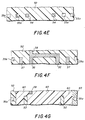
- FIG. 4A a layer 32 of resistive material is first deposited on the surface of substrate 51 in regions that include the eventual heat transfer region.
- metal electrodes 35a and 35b are formed with ends defining the current path through the resistive material at the heating region.
- a layer(s) of diode material 54 is then deposited onto the top of electrodes 35b, see FIG. 4C, and a dielectric passivation layer 52 (e.g. SiO2 or Zr) is deposited over the surface as shown in FIG. 4D.
- a dielectric passivation layer 52 e.g. SiO2 or Zr
- the passivation layer is patterned to reveal portions of electrode 35a and diode 54.
- Zr is used for formation of layer 52 it can be oxidized to form ZrO2.
- the second circuit portion comprising electrodes 37, 38 are then deposited and patterned in the configuration shown in FIG. 4F, and finally the second passivation layer 60 is deposited and patterned to provide a chip having the topography shown in FIG. 4G.
- layer 60 can be polyamide or similar material because it is not overlying the heat transfer path, wherein layer 52 provides the protective cover for the resistive heater elements.
- enable pulses are sequentially applied to terminals 40 and 41.
- the diodes of branch circuits 31a-31c and 31g-31i are forwardly biased and when driver pulses are applied to the terminals 36-A, 36-B in accord with information signals electrodes 35 of those circuits can conduct current through resistive heaters of the circuits to heat overlying ink and effect bubble jetting of an ink drop through their corresponding orifice of orifice plate 18.
- electrode 39 forwardly biasing the diodes of branch circuits 31d-31f and 31j-31L so that driver pulses applied to terminals 36-A and 36-B are transmitted to respective ones of those branch circuits (via coupling electrodes 37) to similarly effect drop ejections in accord with information signal gating the driver circuits.
- circuit construction embodiment described above in accord with the present invention provides the advantages of multiplexing operation without the necessity of patterning two sides of drop ejection chip. Moreover, the circuit constructions of the present invention remove the circuit diode elements from the regions of heat generation. As noted previously, this is particularly important in devices using thin film circuit components which are operated repeatedly at high duty cycles, such as the bubble jet printing devices described above.
- the present invention affords industrial advantages by providing a simple ink jet print head construction for reliable multiplex operation to achieve high density printing.
Landscapes
- Particle Formation And Scattering Control In Inkjet Printers (AREA)
- Non-Adjustable Resistors (AREA)
Abstract
Claims (2)
- Imprimante à jet d'encre à goutte sur demande et du type comportant une pluralité d'orifices, comprenant un dispositif d'éjection de gouttes à film mince comportant une pluralité correspondante d'éléments chauffants d'éjection de gouttes et un moyen de collecteur pour délivrer l'encre auxdits éléments chauffants, dans lequel l'amélioration du dispositif d'éjection de gouttes comprend :(a) un substrat (51) ;(b) une première portion du circuit (31, 35, 36) comprenant une pluralité de branches de circuit qui chacune comporte un élément chauffant résistif (32) et un dispositif de diode (33) formés en relation espacée sur ledit substrat et couplés en série par des lignes d'électrodes de branchement du premier circuit aux régions de borne ;(c) une couche de passivation diélectrique (52) recouvrant la première portion du circuit sauf au niveau des régions de borne discrètes desdites branches de portion de premier circuit ;(d) une seconde portion du circuit (37, 38, 39) comprenant une pluralité de lignes d'électrode de multiplexage recouvrant ladite couche de passivation diélectrique (52) et comportant des sections de connexion se prolongeant à travers ladite couche de passivation (52) en contact avec les régions de borne de la première portion du circuit, et(e) une seconde couche de passivation (60) recouvrant ladite seconde portion du circuit (37, 38, 39) mais ne recouvrant pas lesdits éléments chauffants résistifs.
- Invention selon la revendication 1, dans laquelle ladite première portion du circuit comprend au moins deux branches desdites branches de circuit et ladite seconde portion du circuit comprend :(i) une ligne d'électrodes couplant les côtés d'entrée d'impulsion d'impression desdites branches de circuit à une borne de circuit de puissance commune, et(ii) des ligne d'électrodes séparées couplant respectivement les sorties de diode desdites branches de circuit à des bornes d'activation séparées.
Applications Claiming Priority (2)
| Application Number | Priority Date | Filing Date | Title |
|---|---|---|---|
| US451709 | 1989-12-18 | ||
| US07/451,709 US4999650A (en) | 1989-12-18 | 1989-12-18 | Bubble jet print head having improved multiplex actuation construction |
Publications (2)
| Publication Number | Publication Date |
|---|---|
| EP0458958A1 EP0458958A1 (fr) | 1991-12-04 |
| EP0458958B1 true EP0458958B1 (fr) | 1994-03-30 |
Family
ID=23793392
Family Applications (1)
| Application Number | Title | Priority Date | Filing Date |
|---|---|---|---|
| EP91902342A Expired - Lifetime EP0458958B1 (fr) | 1989-12-18 | 1991-07-12 | Tete d'impression a jet de bulles a structure d'actionnement multiplex amelioree |
Country Status (5)
| Country | Link |
|---|---|
| US (1) | US4999650A (fr) |
| EP (1) | EP0458958B1 (fr) |
| JP (1) | JP2991772B2 (fr) |
| DE (1) | DE69007783T2 (fr) |
| WO (1) | WO1991008899A1 (fr) |
Families Citing this family (40)
| Publication number | Priority date | Publication date | Assignee | Title |
|---|---|---|---|---|
| US5469199A (en) * | 1990-08-16 | 1995-11-21 | Hewlett-Packard Company | Wide inkjet printhead |
| US5648805A (en) * | 1992-04-02 | 1997-07-15 | Hewlett-Packard Company | Inkjet printhead architecture for high speed and high resolution printing |
| US5278584A (en) * | 1992-04-02 | 1994-01-11 | Hewlett-Packard Company | Ink delivery system for an inkjet printhead |
| US5638101A (en) * | 1992-04-02 | 1997-06-10 | Hewlett-Packard Company | High density nozzle array for inkjet printhead |
| US5648804A (en) * | 1992-04-02 | 1997-07-15 | Hewlett-Packard Company | Compact inkjet substrate with centrally located circuitry and edge feed ink channels |
| US5648806A (en) * | 1992-04-02 | 1997-07-15 | Hewlett-Packard Company | Stable substrate structure for a wide swath nozzle array in a high resolution inkjet printer |
| US5563642A (en) * | 1992-04-02 | 1996-10-08 | Hewlett-Packard Company | Inkjet printhead architecture for high speed ink firing chamber refill |
| US5420627A (en) * | 1992-04-02 | 1995-05-30 | Hewlett-Packard Company | Inkjet printhead |
| US5604519A (en) * | 1992-04-02 | 1997-02-18 | Hewlett-Packard Company | Inkjet printhead architecture for high frequency operation |
| US5568171A (en) * | 1992-04-02 | 1996-10-22 | Hewlett-Packard Company | Compact inkjet substrate with a minimal number of circuit interconnects located at the end thereof |
| US5297331A (en) * | 1992-04-03 | 1994-03-29 | Hewlett-Packard Company | Method for aligning a substrate with respect to orifices in an inkjet printhead |
| US5594481A (en) * | 1992-04-02 | 1997-01-14 | Hewlett-Packard Company | Ink channel structure for inkjet printhead |
| DE4214556A1 (de) * | 1992-04-28 | 1993-11-04 | Mannesmann Ag | Elektrothermischer tintendruckkopf |
| US5414245A (en) * | 1992-08-03 | 1995-05-09 | Hewlett-Packard Corporation | Thermal-ink heater array using rectifying material |
| EP0622235B1 (fr) * | 1993-04-30 | 1997-07-30 | Hewlett-Packard Company | Arrangement d'une couche de contact sur une cartouche d'impression en plastique |
| US5956058A (en) * | 1993-11-05 | 1999-09-21 | Seiko Epson Corporation | Ink jet print head with improved spacer made from silicon single-crystal substrate |
| US6003986A (en) * | 1994-10-06 | 1999-12-21 | Hewlett-Packard Co. | Bubble tolerant manifold design for inkjet cartridge |
| US6174046B1 (en) | 1994-10-06 | 2001-01-16 | Hewlett-Packard Company | Reliable contact pad arrangement on plastic print cartridge |
| US5909231A (en) * | 1995-10-30 | 1999-06-01 | Hewlett-Packard Co. | Gas flush to eliminate residual bubbles |
| US5901425A (en) | 1996-08-27 | 1999-05-11 | Topaz Technologies Inc. | Inkjet print head apparatus |
| US6154229A (en) | 1997-10-28 | 2000-11-28 | Hewlett-Packard Company | Thermal ink jet print head and printer temperature control apparatus and method |
| US6575548B1 (en) | 1997-10-28 | 2003-06-10 | Hewlett-Packard Company | System and method for controlling energy characteristics of an inkjet printhead |
| US6476928B1 (en) | 1999-02-19 | 2002-11-05 | Hewlett-Packard Co. | System and method for controlling internal operations of a processor of an inkjet printhead |
| US6318828B1 (en) | 1999-02-19 | 2001-11-20 | Hewlett-Packard Company | System and method for controlling firing operations of an inkjet printhead |
| US6705694B1 (en) | 1999-02-19 | 2004-03-16 | Hewlett-Packard Development Company, Lp. | High performance printing system and protocol |
| US6729707B2 (en) * | 2002-04-30 | 2004-05-04 | Hewlett-Packard Development Company, L.P. | Self-calibration of power delivery control to firing resistors |
| US6435668B1 (en) | 1999-02-19 | 2002-08-20 | Hewlett-Packard Company | Warming device for controlling the temperature of an inkjet printhead |
| US6755495B2 (en) | 2001-03-15 | 2004-06-29 | Hewlett-Packard Development Company, L.P. | Integrated control of power delivery to firing resistors for printhead assembly |
| EP1221372B1 (fr) * | 2001-01-05 | 2005-06-08 | Hewlett-Packard Company | Générateur intégré programmable d'impulsion de commande pour une tête d'impression à jet d'encre |
| US6585339B2 (en) | 2001-01-05 | 2003-07-01 | Hewlett Packard Co | Module manager for wide-array inkjet printhead assembly |
| US6726298B2 (en) | 2001-02-08 | 2004-04-27 | Hewlett-Packard Development Company, L.P. | Low voltage differential signaling communication in inkjet printhead assembly |
| US6478396B1 (en) | 2001-03-02 | 2002-11-12 | Hewlett-Packard Company | Programmable nozzle firing order for printhead assembly |
| US6471320B2 (en) | 2001-03-09 | 2002-10-29 | Hewlett-Packard Company | Data bandwidth reduction to printhead with redundant nozzles |
| US6543879B1 (en) | 2001-10-31 | 2003-04-08 | Hewlett-Packard Company | Inkjet printhead assembly having very high nozzle packing density |
| US6932453B2 (en) * | 2001-10-31 | 2005-08-23 | Hewlett-Packard Development Company, L.P. | Inkjet printhead assembly having very high drop rate generation |
| US6746107B2 (en) | 2001-10-31 | 2004-06-08 | Hewlett-Packard Development Company, L.P. | Inkjet printhead having ink feed channels defined by thin-film structure and orifice layer |
| US6726300B2 (en) * | 2002-04-29 | 2004-04-27 | Hewlett-Packard Development Company, L.P. | Fire pulses in a fluid ejection device |
| US7182422B2 (en) * | 2004-08-23 | 2007-02-27 | Silverbrook Research Pty Ltd | Printhead having first and second rows of print nozzles |
| CN101005951B (zh) | 2004-08-23 | 2010-05-26 | 西尔弗布鲁克研究有限公司 | 对称的喷嘴装置 |
| US7195328B2 (en) * | 2004-08-23 | 2007-03-27 | Silverbrook Res Pty Ltd | Symmetric nozzle arrangement |
Family Cites Families (9)
| Publication number | Priority date | Publication date | Assignee | Title |
|---|---|---|---|---|
| US4463359A (en) * | 1979-04-02 | 1984-07-31 | Canon Kabushiki Kaisha | Droplet generating method and apparatus thereof |
| US4429321A (en) * | 1980-10-23 | 1984-01-31 | Canon Kabushiki Kaisha | Liquid jet recording device |
| CH649040A5 (fr) * | 1982-10-08 | 1985-04-30 | Battelle Memorial Institute | Dispositif pour projeter des gouttelettes d'un liquide electriquement conducteur. |
| US4862197A (en) * | 1986-08-28 | 1989-08-29 | Hewlett-Packard Co. | Process for manufacturing thermal ink jet printhead and integrated circuit (IC) structures produced thereby |
| US4695853A (en) * | 1986-12-12 | 1987-09-22 | Hewlett-Packard Company | Thin film vertical resistor devices for a thermal ink jet printhead and methods of manufacture |
| US4791440A (en) * | 1987-05-01 | 1988-12-13 | International Business Machine Corporation | Thermal drop-on-demand ink jet print head |
| US4847630A (en) * | 1987-12-17 | 1989-07-11 | Hewlett-Packard Company | Integrated thermal ink jet printhead and method of manufacture |
| DE68917790T2 (de) * | 1988-06-03 | 1995-01-05 | Canon Kk | Aufzeichnungskopf mit Flüssigkeitsemission, Substrat hierfür sowie Aufzeichnungsgerät mit Flüssigkeitsemission unter Verwendung dieses Kopfes. |
| DE68928480T2 (de) * | 1988-07-03 | 1998-04-23 | Canon Kk | Tintenstrahlaufzeichnungsvorrichtung |
-
1989
- 1989-12-18 US US07/451,709 patent/US4999650A/en not_active Expired - Fee Related
-
1990
- 1990-12-06 WO PCT/US1990/007141 patent/WO1991008899A1/fr not_active Ceased
- 1990-12-06 DE DE69007783T patent/DE69007783T2/de not_active Expired - Fee Related
- 1990-12-06 JP JP3502708A patent/JP2991772B2/ja not_active Expired - Fee Related
-
1991
- 1991-07-12 EP EP91902342A patent/EP0458958B1/fr not_active Expired - Lifetime
Also Published As
| Publication number | Publication date |
|---|---|
| JP2991772B2 (ja) | 1999-12-20 |
| JPH04503930A (ja) | 1992-07-16 |
| WO1991008899A1 (fr) | 1991-06-27 |
| DE69007783T2 (de) | 1994-10-20 |
| US4999650A (en) | 1991-03-12 |
| EP0458958A1 (fr) | 1991-12-04 |
| DE69007783D1 (de) | 1994-05-05 |
Similar Documents
| Publication | Publication Date | Title |
|---|---|---|
| EP0458958B1 (fr) | Tete d'impression a jet de bulles a structure d'actionnement multiplex amelioree | |
| US4791440A (en) | Thermal drop-on-demand ink jet print head | |
| CA2041544C (fr) | Tete d'impression thermique a jet d'encre goutte a la demande | |
| US5442386A (en) | Structure and method for preventing ink shorting of conductors connected to printhead | |
| US6322200B1 (en) | Decoupled nozzle plate and electrical flexible circuit for an inkjet print cartridge | |
| US5648804A (en) | Compact inkjet substrate with centrally located circuitry and edge feed ink channels | |
| US5984464A (en) | Stable substrate structure for a wide swath nozzle array in a high resolution inkjet printer | |
| US5030971A (en) | Precisely aligned, mono- or multi-color, `roofshooter` type printhead | |
| US5568171A (en) | Compact inkjet substrate with a minimal number of circuit interconnects located at the end thereof | |
| JPH07276643A (ja) | インクジェット記録ヘッド用基板及びそれを用いたヘッド | |
| US4878070A (en) | Thermal ink jet print cartridge assembly | |
| US20030184618A1 (en) | Large thermal ink jet nozzle array printhead | |
| JP2002248778A (ja) | ワイドアレイ・インクジェットプリントヘッドアセンブリ | |
| JP2001080078A (ja) | インクジェットプリントヘッド | |
| US6325491B1 (en) | Inkjet printhead design to reduce corrosion of substrate bond pads | |
| US7445315B2 (en) | Thin film and thick film heater and control architecture for a liquid drop ejector | |
| EP0786343B1 (fr) | Dispositif d'impression thermique par jet d'encre et méthode d'actionnement | |
| US20020126184A1 (en) | Ink jet printhead with large size silicon wafer and relative manufacturing process | |
| WO2008057334A1 (fr) | Tête d'impression de jet d'encre avec conducteur de puissance de retour sur le côté arrière | |
| US6629757B1 (en) | Recording head, substrate therefor, and recording apparatus | |
| EP0742759B1 (fr) | Dispositif d'enregistrement a jet d'encre | |
| JPH0994968A (ja) | インクジェットプリントヘッド | |
| JP3222148B2 (ja) | 熱インク・ジェット・プリントヘッド用多重回路付きインク供給構造および熱インク・ジェット・プリントヘッド | |
| JPH09207346A (ja) | 熱インクジェット記録ヘッドの製造方法 | |
| JPS63247052A (ja) | インクジエツト記録ヘツド |
Legal Events
| Date | Code | Title | Description |
|---|---|---|---|
| PUAI | Public reference made under article 153(3) epc to a published international application that has entered the european phase |
Free format text: ORIGINAL CODE: 0009012 |
|
| AK | Designated contracting states |
Kind code of ref document: A1 Designated state(s): DE FR GB |
|
| 17P | Request for examination filed |
Effective date: 19911202 |
|
| 17Q | First examination report despatched |
Effective date: 19930728 |
|
| GRAA | (expected) grant |
Free format text: ORIGINAL CODE: 0009210 |
|
| AK | Designated contracting states |
Kind code of ref document: B1 Designated state(s): DE FR GB |
|
| REF | Corresponds to: |
Ref document number: 69007783 Country of ref document: DE Date of ref document: 19940505 |
|
| ET | Fr: translation filed | ||
| PLBE | No opposition filed within time limit |
Free format text: ORIGINAL CODE: 0009261 |
|
| STAA | Information on the status of an ep patent application or granted ep patent |
Free format text: STATUS: NO OPPOSITION FILED WITHIN TIME LIMIT |
|
| 26N | No opposition filed | ||
| PGFP | Annual fee paid to national office [announced via postgrant information from national office to epo] |
Ref country code: GB Payment date: 19951110 Year of fee payment: 6 |
|
| PGFP | Annual fee paid to national office [announced via postgrant information from national office to epo] |
Ref country code: FR Payment date: 19951213 Year of fee payment: 6 |
|
| PGFP | Annual fee paid to national office [announced via postgrant information from national office to epo] |
Ref country code: DE Payment date: 19951229 Year of fee payment: 6 |
|
| PG25 | Lapsed in a contracting state [announced via postgrant information from national office to epo] |
Ref country code: GB Effective date: 19961206 |
|
| GBPC | Gb: european patent ceased through non-payment of renewal fee |
Effective date: 19961206 |
|
| PG25 | Lapsed in a contracting state [announced via postgrant information from national office to epo] |
Ref country code: FR Effective date: 19970829 |
|
| PG25 | Lapsed in a contracting state [announced via postgrant information from national office to epo] |
Ref country code: DE Effective date: 19970902 |
|
| REG | Reference to a national code |
Ref country code: FR Ref legal event code: ST |