EP0459314B1 - Datenbus-Klemmschaltung einer Halbleiterspeicheranordnung - Google Patents
Datenbus-Klemmschaltung einer Halbleiterspeicheranordnung Download PDFInfo
- Publication number
- EP0459314B1 EP0459314B1 EP91108445A EP91108445A EP0459314B1 EP 0459314 B1 EP0459314 B1 EP 0459314B1 EP 91108445 A EP91108445 A EP 91108445A EP 91108445 A EP91108445 A EP 91108445A EP 0459314 B1 EP0459314 B1 EP 0459314B1
- Authority
- EP
- European Patent Office
- Prior art keywords
- nmos
- data bus
- circuit
- signal
- data
- Prior art date
- Legal status (The legal status is an assumption and is not a legal conclusion. Google has not performed a legal analysis and makes no representation as to the accuracy of the status listed.)
- Expired - Lifetime
Links
- 239000004065 semiconductor Substances 0.000 title claims description 14
- 230000000295 complement effect Effects 0.000 claims description 21
- 230000003321 amplification Effects 0.000 claims description 14
- 238000003199 nucleic acid amplification method Methods 0.000 claims description 14
- 238000007599 discharging Methods 0.000 claims description 5
- 238000010586 diagram Methods 0.000 description 8
- 230000007704 transition Effects 0.000 description 8
- 230000006866 deterioration Effects 0.000 description 2
- 239000011159 matrix material Substances 0.000 description 1
- 238000012986 modification Methods 0.000 description 1
- 230000004048 modification Effects 0.000 description 1
- 230000004044 response Effects 0.000 description 1
Images


Classifications
-
- G—PHYSICS
- G11—INFORMATION STORAGE
- G11C—STATIC STORES
- G11C11/00—Digital stores characterised by the use of particular electric or magnetic storage elements; Storage elements therefor
- G11C11/21—Digital stores characterised by the use of particular electric or magnetic storage elements; Storage elements therefor using electric elements
- G11C11/34—Digital stores characterised by the use of particular electric or magnetic storage elements; Storage elements therefor using electric elements using semiconductor devices
- G11C11/40—Digital stores characterised by the use of particular electric or magnetic storage elements; Storage elements therefor using electric elements using semiconductor devices using transistors
- G11C11/401—Digital stores characterised by the use of particular electric or magnetic storage elements; Storage elements therefor using electric elements using semiconductor devices using transistors forming cells needing refreshing or charge regeneration, i.e. dynamic cells
- G11C11/4063—Auxiliary circuits, e.g. for addressing, decoding, driving, writing, sensing or timing
- G11C11/407—Auxiliary circuits, e.g. for addressing, decoding, driving, writing, sensing or timing for memory cells of the field-effect type
-
- G—PHYSICS
- G11—INFORMATION STORAGE
- G11C—STATIC STORES
- G11C7/00—Arrangements for writing information into, or reading information out from, a digital store
- G11C7/10—Input/output [I/O] data interface arrangements, e.g. I/O data control circuits, I/O data buffers
- G11C7/1048—Data bus control circuits, e.g. precharging, presetting, equalising
Definitions
- the present invention relates to a data bus clamping circuit in a semiconductor memory device such as a dynamic RAM (Random Access Memory) capable of reading out data on a data bus at high speed, independently of variation in a power supply voltage, with a differential amplification type of read out circuit.
- a dynamic RAM Random Access Memory
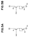
- FIGS. 5A and 5B show conventional data bus clamping circuits used, for instance, in a semiconductor memory device as shown in FIG. 2, which will be explained later in detail.
- the data bus clamping circuit of FIGS. 5A and 5B comprises an N channel type of MOS transistors (referred to as NMOS's hereinafter) 61, 62, 63 and 64 which are extremely small in mutual conductance.
- NMOS's 61 and 62 are connected in series between a data bus DB and a ground potential VSS.
- NMOS's 63 and 64 are connected in series between a data bus DB ⁇ and the ground potential VSS.
- NMOS's 61 and 63 are operative to turn on and off in response to a row address latch signal RAS. When NMOS's 61 and 63 turn on, NMOS's 62 and 64 are operative to turn on.
- FIG. 6 is a view showing operational wave forms at the time when data are read out by the data bus clamping circuits of FIGS. 5A and 5B. Now referring to FIG. 6, a readout operation for memory cell array 10 shown in FIG. 2 will be explained hereinafter.
- the row address latch signalRAS is in level VSS
- both sense amplifier enabling signalsSAP and SAN are in 1/2 VCCH (power supply voltage)
- a column address decoder enabling signal YDE and a column decoding signal YD are in VSS
- bit lines BL and BL ⁇ are in 1/2 VCCH.
- NMOS's 61 and 63 in the data bus clamping circuits of FIGS. 5A and 5B are in a turn-off condition.
- a data bus pull-up circuit 50 a circuit structure of which is shown in FIGS. 4A and 4B, NMOS's 51 and 52 each having a threshold voltage Vt are in a turn-on condition, and thus the data buses DB and DB ⁇ are (VCCH - Vt) in the potential.
- the row address latch signal RAS becomes VCCH.
- a row direction of the memory cell array 10 is selected by a row address decoder 20, so that data on the selected memory cells are read out on the bit lines BL and BL ⁇ .
- the sense amplifier enabling signal SAP changes in level from 1/2 VCCH to VCCL and the sense amplifier enabling signal SAN changes in level from 1/2 VCCH to VSS.
- Those transitions of potential level cause a sense amplifier circuit 30 to amplify a minute potential difference ⁇ V between the bit lines BL and BL ⁇ .
- a column address signal YADn is selected by a certain column address decoder 40 selected in VCCL, and the column decoding signal YD changes in level from VSS to VCCL.
- NMOS's 43 and 44 in the column address decoder 40 become a turn-on condition to transfer data on the bit lines BL and BL ⁇ to the data bus DB and DB ⁇ .
- produced is a potential difference corresponding to the bit line data between the complementary data bus DB and DB ⁇ .
- Such a potential difference is amplified by a differential amplification type of readout circuit 70, and then be output as a readout data DOUT.
- the row address latch signal RAS is in level VSS, so that the data bus clamping circuit of FIG. 5A or 5B turns off. Further, at that time, the column address decoder enabling signal YDE and the column decoding signal YD become VSS.
- the data bus DB and DB ⁇ are electrically separated from the data bus clamping circuit and the bit lines BL and BL ⁇ , and the data bus DB and DB ⁇ become in potential (VCC - Vt) by the data bus pull-up circuit 50.
- transition of the row address strobe signal RAS ⁇ from "L” to “H” causes both the sense amplifier enabling signals SAP and SAN to be in 1/2 VCCL, and also causes both the bit lines BL and BL ⁇ to be in 1/2 VCCL. Thus, a series of reading out operation is terminated.
- the differential amplification type of readout circuit 70 is provided with optimum potential set values VA and VB for a high speed amplification. Whereas, at time t in FIG. 6, when the differential amplification type of readout circuit 70 starts an amplification operation, the potentials of the data buses DB and DB ⁇ have not descended up to the optimum potential set values VA and VB, respectively. Accordingly, the differential amplification type of readout circuit 70 can not amplify at high speed the data on the data buses DB and DB ⁇ . Thus, the conventional data bus clamping circuit has been associated with such a problem that a readout speed of data slows.
- the potentials of the data buses DB and DB ⁇ are clamped at high speed by the data bus clamping circuit.
- a current of the sense amplifier enabling signal SAP flows through P channel type of MOS transistor (referred to as PMOS hereinafter) 34 in the sense amplifier 30, NMOS 44 in the column address decoder 40 and NMOS's 63 and 64 in the data bus clamping circuits in FIGS. 5A and 5B to the earth potential VSS.
- PMOS P channel type of MOS transistor
- Increment of such a current brings drawbacks such as deterioration of the transistors as well as increment of an amount of consumption current.
- the mutual conductance of NMOS's 61-64 is set to be small. In other words, a large turn-on resistance is provided for decrement of such a current. Consequently, it is impossible to clamp the potentials of the data buses DB and DB ⁇ at high speed by the data bus clamping circuit, and thus impossible to solve the problem with which the conventional device encounters.
- a data bus clamping circuit according to the present invention is disclosed in claim 1.
- Claims 2 to 8 disclose further embodiments of the present invention.
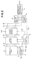
- FIG. 2 shows exemplarily a semiconductor memory device such as a dynamic RAM (Random Access Memory) to which a data bus clamping circuit according to the present invention is applicable.
- This semiconductor memory device is provided with a memory cell array 10 in which a large number of memory cells are arranged in a matrix configuration.
- the memory cell array 10 is coupled through a plurality of word lines WL with a row address decoder 20, and further coupled through a plurality of complementary bit lines BL and BL ⁇ with a sense amplifier 30 and a column address decoder 40.
- the column address decoder 40 is connected to a plurality of complementary data buses DB and DB ⁇ .
- the row address decoder 20 decodes a plurality of row address signals XADm taken in by a row address strobe signal RAS ⁇ to select memory cells in a row direction of the memory cell array 10 through the word lines WL.
- the sense amplifier 30 amplifies readout data on the bit lines BL and BL ⁇ , based on sense amplifier enabling signals SAP and SAN.
- the column address decoder 40 decodes a plurality of column address signals YADn based on a column address decoder enabling signal YDE to select memory cells in a column direction of the memory cell array 10.
- the data bus pull-up circuit 50 usually pulls up the data buses DB and DB ⁇ .
- the data bus clamping circuit 60 clamps the data buses DB and DB ⁇ to a predetermined potential based on a row address latch signal RAS.
- the differential amplification type of readout circuit 70 amplifies on a differential basis a potential difference between the complementary data buses DB and DB ⁇ and outputs readout data DOUT in a MOS level.
- This semiconductor memory device is provided with a control signal generating circuit 80 for control of the device.
- the control signal generating circuit 80 generates, based on the row address strobe signal RAS ⁇ the row address latch signal RAS, the column address decoder enabling signal YDE, and sense amplifier enabling signals SAP and SAN.
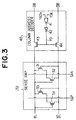
- FIG. 3 is a circuit diagram exemplarily showing structure of the sense amplifier 30 and the column address decoder 40 in FIG. 2.
- the sense amplifier 30 is a flip-flop circuit comprising NMOS's 31 and 32 and PMOS's 33 and 34 for amplifying a potential difference between the complementary bit lines BL and BL ⁇ .
- NMOS 31 is connected between the bit line BL and the sense amplifier enabling signal SAN, and its gate is connected to the bit line BL ⁇ .
- NMOS 32 is connected between the bit line BL ⁇ and the sense amplifier enabling signal SAN, and its gate is connected to the bit line BL.
- PMOS 33 is connected between the bit line BL and the sense amplifier enabling signal SAP, and its gate is connected to the bit line BL ⁇ .
- PMOS 34 is connected between the bit line BL ⁇ and the sense amplifier enabling signal SAP, and its gate is connected to the bit line BL.
- the column address decoder 40 includes NAND gate 41 to which the column address signals YADn and the column address decoder enabling signal YDE are entered.
- An output of NAND gate 41 is connected through an inverter 42 to the respective gates of NMOS's 43 and 44.
- NMOS's 43 and 44 are operable to turn on or off in accordance with a column decoding signal YD output from the inverter 42, and be connected between the bit line BL and the data bus DB, and between the bit line BL ⁇ and the data bus DB ⁇ , respectively.
- FIGS. 4A and 4B are circuit diagrams exemplarily showing structures of the data bus pull-up circuit 50 in FIG. 2.
- the data bus pull-up circuit 50 comprises NMOS's 51 and 52 which are small in mutual conductance.
- a source of NMOS 51 is connected to the data bus DB ⁇ .
- Drain and gate of NMOS 51 are connected to the power supply potential VCC, respectively.
- a source of NMOS 52 is connected to the data bus DB.
- NMOS 52 has a drain and a gate connected to the power supply potential VCC.
- FIG. 1 is a circuit diagram of an illustrative embodiment of a data bus clamping circuit. This data bus clamping circuit may be substituted for the conventional data bus clamping circuit 60, which has been explained above referring to FIGS. 5A and 5B as prior art.
- the data bus clamping circuit in FIG. 1 comprises a first discharge circuit 100 for usually discharging the complementary data buses DB and DB ⁇ in FIG. 2 with a small discharge ability so that the data buses DB and DB ⁇ are clamped, a second discharge circuit 110 for discharging the data buses DB and DB ⁇ with a discharge ability larger than the first discharge circuit 100, during a period of time from the time a standby period is terminated until the time the column address decoder 40 in FIG. 2 is enabled, so that the data buses DB and DB ⁇ are clamped, and a control circuit 120 for controlling an operation of the second discharge circuit 110 by a clamp signal CLP.
- the first discharge circuit 100 is provided with NMOS's 101, 102, 103 and 104 which are designed to provide small mutual conductance gml.
- NMOS 101 Connected to the complementary data bus DB shown in FIG. 2 is a drain electrode of NMOS 101, of which a gate electrode is connected to the row address latch signal RAS shown in FIG. 2.
- a source electrode of NMOS 101 is connected to drain and gate electrodes of NMOS 102, of which a source electrode is connected to the earth potential VSS.
- Connected to the other data bus DB ⁇ is a drain electrode of NMOS 103, of which a gate electrode is connected to the row address latch signal RAS.
- a source electrode of NMOS 103 is connected to drain and gate electrodes of NMOS 104, of which a source electrode is connected to the earth potential VSS.
- the second discharge circuit 110 is provided with NMOS's 111, 112, 113 and 114 which are designed to provide relatively large mutual conductance gm2.
- Connected to the complemental data bus DB is a drain electrode of NMOS 111, of which a gate electrode is connected to the clamp signal CLP and a gate electrode of NMOS 113.
- a source electrode of NMOS 111 is connected to drain and gate electrodes of NMOS 112, of which a source electrode is connected to the earth potential VSS.
- the source electrode of NMOS 111 is also connected to drain and gate electrodes of NMOS 114.
- Connected to the other data bus DB ⁇ is a drain electrode of NMOS 113, of which a source electrode is connected to the drain electrode of NMOS 114.
- the mutual conductance gm1 of NMOS's 101, 102, 103 and 104 in the first discharge circuit 100 and the mutual conductance gm2 of NMOS's 111, 112, 113 and 114 in the second discharge circuit 110 are set to be approximately in the ratio 1 : 10 to 20.
- the control circuit 120 for controlling the second discharge circuit 110 comprises an inverter 121 for entering the row address latch signal RAS output from the control signal generating circuit 80 in FIG. 2 and an NOR gate 122 for entering an output of the inverter 121 and the column address decoder enabling signal YDE.
- the clamp signal CLP output from the NOR gate 122 is supplied to the respective gates of NMOS's 111 and 113 in the second discharge circuit 110.
- FIG. 7 shows operational waveforms at the time when data are read out by the data bus clamping circuit of FIG. 1. Now referring to FIG. 7, a readout operation for memory cell array 10 shown in FIG. 2 will be explained hereinafter.
- NMOS's 101-104 in the first discharge circuit 100 shown in FIG. 1 are in a turn-off condition, and also NMOS's 111-114 in the second discharge circuit 110 are in a turn-off condition, since the clamp signal CLP output from the control circuit 120 is in VSS.
- NMOS's 51 and 52 each having a threshold voltage Vt are in a turn-on condition, and thus the data buses DB and DB ⁇ are set to be (VCCH - Vt) in the potential.
- the row address latch signal RAS which is output from the control signal generating circuit 80, changes from VSS to VCCH in the level.
- the row address latch signal RAS becomes VCCH, a row direction of the memory cell array 10 is selected by a row address decoder 20 in FIG. 2, so that data on the selected memory cells are read out on the bit lines BL and BL ⁇ .
- the electric charge on the data buses DB and DB ⁇ is further discharged by the data bus clamping circuit of FIG. 1.
- the potentials of the data buses DB and DB ⁇ are determined between VCCH and VSS based on the resistive divisional ratio of turn-on resistance of NMOS's 51 and 52 in the data bus pull-up circuit 50 in FIG. 4 to turn-on resistance of NMOS's 101-104 and 111-114 in the first and second discharge circuits 100 and 110 in FIG. 1.
- the sense amplifier enabling signal SAP which is output from the control signal generating circuit 80, changes in level from 1/2 VCCH to VCCL and the sense amplifier enabling signal SAN changes in level from 1/2 VCCH to VSS. Those transitions of potential level cause a sense amplifier circuit 30 to amplify a minute potential difference ⁇ V between the bit lines BL and BL ⁇ .
- NMOS's 111-114 in the second discharge circuit 110 are in a turn-off condition.
- a column address signal YADn is selected by a certain column address decoder 40 in FIG. 3 selected in VCCL, and the column decoding signal YD changes in level from VSS to VCCL.
- NMOS's 43 and 44 in the column address decoder 40 become a turn-on condition to transfer data on the bit lines BL and BL ⁇ to the data bus DB and DB ⁇ .
- produced is a potential difference corresponding to the bit line data between the complementary data bus DB and DB ⁇ .
- Such a potential difference is amplified by a differential amplification type of readout circuit 70, and then be output as a readout data DOUT.
- the row address latch signal RAS which is output from the control signal generating circuit 80 in FIG. 2, is in level VSS, so that NMOS's 101-104 in the first discharge circuit 100 shown in FIG. 1 are in a turn-off condition. Further, at that time, the column address decoder enabling signal YDE and the column decoding signal YD become VSS.
- the data buses DB and DB ⁇ are electrically separated from the data bus clamping circuit of FIG.
- the data bus clamping circuit in FIG. 1 comprises first and second discharge circuits 100 and 110, wherein NMOS's 101-104 in the first discharge circuit 100 are designed to provide small mutual conductance gm1, and NMOS's 111-114 of the second discharge circuit 110 are designed to provide relatively large mutual conductance gm2.
- the second discharge circuit 110 are control led by the clamp signal CLP output from the control circuit 120 to clamp the data buses DB and DB ⁇ from the time active period Tb starts until the time just before the data on the bit lines BL and BL ⁇ are transferred to the data buses DB and DB ⁇ upon occurrence of transition of the column decoding signal YD in level from VSS to VCCL.
- This arrangement makes it possible to set the data buses DB and DB ⁇ to an optimum potential which may be amplified at high speed by the differential amplification type of readout circuit 70, thereby providing a high speed data readout.
- the second discharge circuit 110 clamps the data buses DB and DB ⁇ from the time active period Tb starts until the time just before the data on the bit lines BL and BL ⁇ are transferred to the data buses DB and DB ⁇ . Consequently, there is no such a matter that a large current of the sense amplifier enabling signal SAP in FIG. 3 flows through PMOS 34 into the sense amplifier 30, NMOS 44 in the column address decoder 40 and NMOS's 103 and 104 in the first discharge circuit 100 in the data bus clamping circuit to the earth potential VSS.
- NMOS's 103 and 104 are designed to provide small mutual conductance gm1 (in other word, turn-on resistance is large), it is possible to prevent a large current from flowing, thereby reducing a consumption current and also avoiding affection such as deterioration of the transistors.
Landscapes
- Engineering & Computer Science (AREA)
- Microelectronics & Electronic Packaging (AREA)
- Computer Hardware Design (AREA)
- Dram (AREA)
Claims (8)
- Datenbus-Klemmschaltung zur Verwendung in einer Halbleiterspeicheranordnung, mit einem Speicherzellenarray (10) zum Speichern von Daten, einem Zeilenadressendecoder (20) zum Decodieren von Zeilenadressensignalen (XADm) basierend auf einem ersten Signal (


- Datenbus-Klemmschaltung nach Anspruch 1, gekennzeichnet durch eine Steuerschaltung (120) zum Steuern einer Operation der zweiten Entladeschaltung (110) durch ein Klemmsignal (CLP).
- Datenbus-Klemmschaltung nach Anspruch 1, dadurch gekennzeichnet, daß die erste Entladeschaltung (100) mit einem ersten, zweiten, dritten und vierten MOS-Transistor (NMOS 101, 102, 103 und 104) versehen ist, die so ausgebildet sind, daß sie eine relativ kleine Steilheit gm1 aufweisen, mit einem der komplementären Datenbusse eine Drain-Elektrode des ersten MOS-Transistors (NMOS 101) verbunden ist, bei dem eine Gate-Elektrode mit dem ersten Signal (RAS) verbunden ist, eine Source-Elektrode des ersten MOS-Transistors (NMOS 101) mit der Drain- und Gate-Elektrode des zweiten MOS-Transistors (NMOS 102) verbunden ist, bei dem eine Source-Elektrode mit Massepotential (VSS) verbunden ist, mit dem anderen Datenbus (

- Datenbus-Klemmschaltung nach Anspruch 1 oder 2, dadurch gekennzeichnet, daß die zweite Entladeschaltung (110) mit einem fünften, sechsten, siebten und achten MOS-Transistor (NMOS 111, 112, 113 und 114) versehen ist, die so ausgebildet sind, daß sie eine relativ große Steilheit gm2 aufweisen, mit einem der komplementären Datenbusse eine Drain-Elektrode des fünften MOS-Transistors (NMOS 111) verbunden ist, bei dem eine Gate-Elektrode mit einem Klemmsignal (CLP) und einer Gate-Elektrode des siebten MOS-Transistors (NMOS 113) verbunden ist, eine Source-Elektrode des fünften MOS-Transistors (NMOS 111) mit der Drain- und Gate-Elektrode des sechsten MOS-Transistors (NMOS 112) verbunden ist, bei dem eine Source-Elektrode mit dem Massepotential (VSS) verbunden ist, die Source-Elektrode des fünften MOS-Transistors (NMOS 111) auch mit der Drain- und Gate-Elektrode des achten MOS-Transistors (NMOS 114) verbunden ist, und mit dem anderen Datenbus (

- Datenbus-Klemmschaltung nach Anspruch 1, dadurch gekennzeichnet, daß die erste Entladeschaltung (100) mit einem ersten, zweiten, dritten und vierten MOS-Transistor (NMOS 101, 102, 103 und 104) versehen ist, die so ausgebildet sind, daß sie eine relativ kleine Steilheit gm1 aufweisen, und die zweite Entladeschaltung (110) mit einem fünften, sechsten, siebten und achten MOS-Transistor (NMOS 111, 112, 113 und 114) versehen sind, die so ausgebildet sind, daß sie eine relativ große Steilheit gm2 aufweisen, wobei die Steilheit gm1 des ersten, zweiten, dritten und vierten MOS-Transistors (NMOS 101, 102, 103 und 104) in der ersten Entladeschaltung (100) und die Steilheit gm2 des fünften, sechsten, siebten und achten MOS-Transistors (NMOS 111 , 112, 113 und 114) in der zweiten Entladeschaltung (110) ungefähr auf das Verhältnis 1 : 10 bis 20 gesetzt werden.
- Datenbus-Klemmschaltung nach Anspruch 2, dadurch gekennzeichnet, daß die Halbleiterspeicheranordnung eine Steuersignalerzeugungsschaltung (80) umfaßt, und die Steuerschaltung (120) einen Inverter (121) zum Einspeisen eines von der Steuersignalerzeugungsschaltung (80) ausgegebenen Zeilenadressen-Latchsignals (RAS) und ein NOR-Gatter (122) zum Einspeisen eines Ausgangssignals des Inverters (121) und des Spaltenadressendecoderfreigabesignals (YDE) und zum Ausgeben des Klemmsignals (CLP) aufweist.
- Datenbus-Klemmschaltung nach einem der Ansprüche 3, 4, 5 und 7, dadurch gekennzeichnet, daß jeder der MOS-Transistoren ein N-Kanal-MOS-Transistor ist.
- Halbleiterspeicheranordnung mit einem Speicherzellenarray (10) zum Speichem von Daten, einem Zeilenadressendecoder (20) zum Decodieren von Zeilenadressensignalen (XADm) basierend auf einem ersten Signal (


Applications Claiming Priority (2)
| Application Number | Priority Date | Filing Date | Title |
|---|---|---|---|
| JP142664/90 | 1990-05-31 | ||
| JP2142664A JPH0438697A (ja) | 1990-05-31 | 1990-05-31 | 半導体記憶装置のデータバスクランプ回路 |
Publications (3)
| Publication Number | Publication Date |
|---|---|
| EP0459314A2 EP0459314A2 (de) | 1991-12-04 |
| EP0459314A3 EP0459314A3 (en) | 1992-10-28 |
| EP0459314B1 true EP0459314B1 (de) | 1996-09-11 |
Family
ID=15320627
Family Applications (1)
| Application Number | Title | Priority Date | Filing Date |
|---|---|---|---|
| EP91108445A Expired - Lifetime EP0459314B1 (de) | 1990-05-31 | 1991-05-24 | Datenbus-Klemmschaltung einer Halbleiterspeicheranordnung |
Country Status (5)
| Country | Link |
|---|---|
| US (1) | US5091886A (de) |
| EP (1) | EP0459314B1 (de) |
| JP (1) | JPH0438697A (de) |
| KR (1) | KR100203717B1 (de) |
| DE (1) | DE69121967T2 (de) |
Families Citing this family (13)
| Publication number | Priority date | Publication date | Assignee | Title |
|---|---|---|---|---|
| US5260904A (en) * | 1990-05-31 | 1993-11-09 | Oki Electric Industry Co., Ltd. | Data bus clamp circuit for a semiconductor memory device |
| JPH0474382A (ja) * | 1990-07-17 | 1992-03-09 | Fujitsu Ltd | 半導体記憶装置 |
| US5206550A (en) * | 1991-06-20 | 1993-04-27 | Texas Instruments, Incorporated | Amplifier with actively clamped load |
| JPH05342872A (ja) * | 1992-06-05 | 1993-12-24 | Oki Micro Design Miyazaki:Kk | 半導体記憶装置 |
| TW223172B (en) * | 1992-12-22 | 1994-05-01 | Siemens Ag | Siganl sensing circuits for memory system using dynamic gain memory cells |
| KR0133973B1 (ko) * | 1993-02-25 | 1998-04-20 | 기다오까 다까시 | 반도체 기억장치 |
| KR0158027B1 (ko) * | 1993-12-29 | 1999-02-01 | 모리시다 요이치 | 반도체집적회로 |
| JP3248482B2 (ja) * | 1998-03-13 | 2002-01-21 | 日本電気株式会社 | 半導体記憶装置 |
| AU2003295880A1 (en) * | 2002-11-27 | 2004-06-23 | University Of Toledo, The | Integrated photoelectrochemical cell and system having a liquid electrolyte |
| US7667133B2 (en) * | 2003-10-29 | 2010-02-23 | The University Of Toledo | Hybrid window layer for photovoltaic cells |
| WO2006110613A2 (en) * | 2005-04-11 | 2006-10-19 | The University Of Toledo | Integrated photovoltaic-electrolysis cell |
| DE102005029872A1 (de) * | 2005-06-27 | 2007-04-19 | Infineon Technologies Ag | Speicherzelle, Lesevorrichtung für die Speicherzelle sowie Speicheranordnungen mit einer derartigen Speicherzelle und Lesevorrichtung |
| US7417903B2 (en) * | 2005-09-29 | 2008-08-26 | Hynix Semiconductor Inc. | Core voltage generator and method for generating core voltage in semiconductor memory device |
Family Cites Families (4)
| Publication number | Priority date | Publication date | Assignee | Title |
|---|---|---|---|---|
| JPS6194296A (ja) * | 1984-10-16 | 1986-05-13 | Fujitsu Ltd | 半導体記憶装置 |
| US4694429A (en) * | 1984-11-29 | 1987-09-15 | Kabushiki Kaisha Toshiba | Semiconductor memory device |
| JPS62134894A (ja) * | 1985-12-06 | 1987-06-17 | Mitsubishi Electric Corp | 半導体記憶装置 |
| US4961168A (en) * | 1987-02-24 | 1990-10-02 | Texas Instruments Incorporated | Bipolar-CMOS static random access memory device with bit line bias control |
-
1990
- 1990-05-31 JP JP2142664A patent/JPH0438697A/ja active Pending
-
1991
- 1991-04-16 KR KR1019910006085A patent/KR100203717B1/ko not_active Expired - Fee Related
- 1991-05-24 DE DE69121967T patent/DE69121967T2/de not_active Expired - Fee Related
- 1991-05-24 EP EP91108445A patent/EP0459314B1/de not_active Expired - Lifetime
- 1991-05-28 US US07/706,206 patent/US5091886A/en not_active Expired - Lifetime
Also Published As
| Publication number | Publication date |
|---|---|
| DE69121967D1 (de) | 1996-10-17 |
| US5091886A (en) | 1992-02-25 |
| DE69121967T2 (de) | 1997-03-27 |
| JPH0438697A (ja) | 1992-02-07 |
| KR100203717B1 (ko) | 1999-06-15 |
| EP0459314A2 (de) | 1991-12-04 |
| KR910020728A (ko) | 1991-12-20 |
| EP0459314A3 (en) | 1992-10-28 |
Similar Documents
| Publication | Publication Date | Title |
|---|---|---|
| US4750155A (en) | 5-Transistor memory cell which can be reliably read and written | |
| US5243573A (en) | Sense amplifier for nonvolatile semiconductor storage devices | |
| US5574687A (en) | Semiconductor memory | |
| EP0459314B1 (de) | Datenbus-Klemmschaltung einer Halbleiterspeicheranordnung | |
| JPH02201797A (ja) | 半導体メモリ装置 | |
| US4733112A (en) | Sense amplifier for a semiconductor memory device | |
| US4825110A (en) | Differential amplifier circuit | |
| EP0388176B1 (de) | Halbleiter-Speichereinrichtung | |
| JPH0750556A (ja) | フリップフロップ型増幅回路 | |
| US5260904A (en) | Data bus clamp circuit for a semiconductor memory device | |
| US5506522A (en) | Data input/output line sensing circuit of a semiconductor integrated circuit | |
| US5699305A (en) | Amplifier and semiconductor memory device having the same | |
| US4451907A (en) | Pull-up circuit for a memory | |
| US4467456A (en) | Memory circuit | |
| KR950005171B1 (ko) | 전류 미러 증폭회로 및 그의 구동 방법 | |
| KR940004516B1 (ko) | 반도체 메모리의 고속 센싱장치 | |
| EP0148364B1 (de) | Zeitsignalgenerator | |
| JP2527050B2 (ja) | 半導体メモリ用センスアンプ回路 | |
| EP0170781B1 (de) | Dynamische MOS-Speicheranordnung | |
| JPH0660665A (ja) | 半導体スタティックramのビット線負荷回路 | |
| US6181623B1 (en) | Semiconductor MOS/BIPOLAR composite transistor and semiconductor memory device using the same | |
| EP0462866B1 (de) | Halbleiterspeicheranordnung | |
| JPS5819791A (ja) | 半導体記憶装置 | |
| EP0149403A2 (de) | Leseverstärker für statischen MOS-Speicher | |
| US5565802A (en) | Semiconductor device with differential amplifier operable at high speed |
Legal Events
| Date | Code | Title | Description |
|---|---|---|---|
| PUAI | Public reference made under article 153(3) epc to a published international application that has entered the european phase |
Free format text: ORIGINAL CODE: 0009012 |
|
| AK | Designated contracting states |
Kind code of ref document: A2 Designated state(s): DE FR NL |
|
| PUAL | Search report despatched |
Free format text: ORIGINAL CODE: 0009013 |
|
| AK | Designated contracting states |
Kind code of ref document: A3 Designated state(s): DE FR NL |
|
| 17P | Request for examination filed |
Effective date: 19930428 |
|
| 17Q | First examination report despatched |
Effective date: 19950428 |
|
| GRAH | Despatch of communication of intention to grant a patent |
Free format text: ORIGINAL CODE: EPIDOS IGRA |
|
| GRAA | (expected) grant |
Free format text: ORIGINAL CODE: 0009210 |
|
| GRAH | Despatch of communication of intention to grant a patent |
Free format text: ORIGINAL CODE: EPIDOS IGRA |
|
| AK | Designated contracting states |
Kind code of ref document: B1 Designated state(s): DE FR NL |
|
| REF | Corresponds to: |
Ref document number: 69121967 Country of ref document: DE Date of ref document: 19961017 |
|
| ET | Fr: translation filed | ||
| PLBE | No opposition filed within time limit |
Free format text: ORIGINAL CODE: 0009261 |
|
| STAA | Information on the status of an ep patent application or granted ep patent |
Free format text: STATUS: NO OPPOSITION FILED WITHIN TIME LIMIT |
|
| 26N | No opposition filed | ||
| PGFP | Annual fee paid to national office [announced via postgrant information from national office to epo] |
Ref country code: FR Payment date: 20020508 Year of fee payment: 12 |
|
| PGFP | Annual fee paid to national office [announced via postgrant information from national office to epo] |
Ref country code: NL Payment date: 20020529 Year of fee payment: 12 Ref country code: DE Payment date: 20020529 Year of fee payment: 12 |
|
| PG25 | Lapsed in a contracting state [announced via postgrant information from national office to epo] |
Ref country code: NL Free format text: LAPSE BECAUSE OF NON-PAYMENT OF DUE FEES Effective date: 20031201 |
|
| PG25 | Lapsed in a contracting state [announced via postgrant information from national office to epo] |
Ref country code: DE Free format text: LAPSE BECAUSE OF NON-PAYMENT OF DUE FEES Effective date: 20031202 |
|
| PG25 | Lapsed in a contracting state [announced via postgrant information from national office to epo] |
Ref country code: FR Free format text: LAPSE BECAUSE OF NON-PAYMENT OF DUE FEES Effective date: 20040130 |
|
| NLV4 | Nl: lapsed or anulled due to non-payment of the annual fee |
Effective date: 20031201 |
|
| REG | Reference to a national code |
Ref country code: FR Ref legal event code: ST |