EP0459521A2 - Dispositif de mémoire à semi-conducteur ayant un circuit de redondance - Google Patents
Dispositif de mémoire à semi-conducteur ayant un circuit de redondance Download PDFInfo
- Publication number
- EP0459521A2 EP0459521A2 EP91108972A EP91108972A EP0459521A2 EP 0459521 A2 EP0459521 A2 EP 0459521A2 EP 91108972 A EP91108972 A EP 91108972A EP 91108972 A EP91108972 A EP 91108972A EP 0459521 A2 EP0459521 A2 EP 0459521A2
- Authority
- EP
- European Patent Office
- Prior art keywords
- data
- circuit
- redundancy
- output
- memory cell
- Prior art date
- Legal status (The legal status is an assumption and is not a legal conclusion. Google has not performed a legal analysis and makes no representation as to the accuracy of the status listed.)
- Granted
Links
Images




Classifications
-
- G—PHYSICS
- G11—INFORMATION STORAGE
- G11C—STATIC STORES
- G11C29/00—Checking stores for correct operation ; Subsequent repair; Testing stores during standby or offline operation
-
- G—PHYSICS
- G11—INFORMATION STORAGE
- G11C—STATIC STORES
- G11C29/00—Checking stores for correct operation ; Subsequent repair; Testing stores during standby or offline operation
- G11C29/70—Masking faults in memories by using spares or by reconfiguring
- G11C29/78—Masking faults in memories by using spares or by reconfiguring using programmable devices
- G11C29/84—Masking faults in memories by using spares or by reconfiguring using programmable devices with improved access time or stability
-
- G—PHYSICS
- G11—INFORMATION STORAGE
- G11C—STATIC STORES
- G11C29/00—Checking stores for correct operation ; Subsequent repair; Testing stores during standby or offline operation
- G11C29/70—Masking faults in memories by using spares or by reconfiguring
- G11C29/86—Masking faults in memories by using spares or by reconfiguring in serial access memories, e.g. shift registers, CCDs, bubble memories
Definitions
- This invention relates to a semiconductor memory device and, more particularly, to a redundancy circuit provided in a semiconductor memory device used especially for an image or video data processing operation to temporarily store data supplied in a bit-serial manner and then read out the stored data in a bit-serial manner.
- the semiconductor memory includes an input circuit provided with a shift register having a plurality of data storage and shift stages necessary to hold the video data for one line. Since the video data for one line are read out in a bit-serial manner, the semiconductor memory device also includes an output circuit provided with a data register or a shift register having a plurality of storage stages necessary to hold those data.
- a memory cell array comprising groups of memory cells corresponding to a plurality of lines, each memory cell group storing one-line data being taken as an unit, between the shift register in the input circuit (referred to as “write shift register” hereinafter) and the data register or shift register in the data output circuit (referred to as “read data register” or “read shift register” hereinafter). Any memory cell group is selected by a word line.
- Data to be processed are inputted in bit-serial way into the write shift register. Once one-line data are each held in one place of this register, respectively, these data are in parallel transferred to the memory cell array, and stored in the memory cell group selected by the word line.
- the one-line data stored in the memory cell array are selected by the word line and in parallel transferred under a specified timing to the read data register and each held in one place of it, respectively. These data held in the places of the read data register are, under the control of a control signal from the output control circuit, transferred in the bit-serial manner to the output bus and outputted from the output terminal.
- one-line data from the memory cell array are transferred to and held in the read shift register and then outputted in the bit-serial manner from the last stage of the shift register to the output bus.
- a redundancy circuit for replacing defective memory cell(s) in the memory cell array with normal memory cell(s) to thereby prevent the memory chip from being rejected.
- This redundancy circuit configuration is similar to above-stated configuration except the number of stages in each circuit, and comprises a redundancy write shift register, a redundancy memory cell array, and either a redundancy read data register with the associated output circuit or a redundancy read shift register, which correspond to the above-described regular shift register, regular memory cell array, and either regular read data register with the associated output control circuit or regular read shift register, respectively.
- the number of the stages or columns in each redundancy circuit is determined taking a predicted number of memory cells in the regular memory cell array which may be failed, the size of the memory chip, economical respect, etc. into consideration.
- this redundancy circuit particularly with an output circuit consisting of a data register, will be described below.
- data to be proceeded is inputted in the bit-serial manner into the regular write shift register and sequentially held in each stage thereof.
- the data written in a failed memory cell when found, in the regular memory cell array is inputted and held in the redundancy write register as well.
- the redundancy write shift register when a plurality of failed memory cells are found in one line, the following data inputted thereinto is held in the first place, and the data of each place, if already held, is shifted to the next place.
- a read mode from the regular memory cell array and the redundancy memory cell array, respective one-line data are synchronously transferred to, and held in, the regular read data register and the redundancy read data register, respectively.
- the data held in the stages of the regular read-data register are in sequence transferred to the output bus under the control of output control signals from the regular output control circuit.
- This transfer is carried out in the order of the first place to the last.
- the data transfer from regular read data register to the output bus moves to the stage corresponding to a defective memory cell, the data transfer from the regular read data register is interrupted, and instead the data transfer from the redundancy read data register to the output bus is carried out.
- This transfer of data from the redundancy read data register are performed in the same order as in the input of them under the control of output control signals from the redundancy output control circuit.
- the data corresponding to failed memory cells are held in sequence in the first places of the redundancy write shift register, and in turn transferred to and stored in, the redundancy memory cell array, and read out, and held similarly in the first places of the redundancy read data register.
- the number of failed or faulty memory cells varies among semiconductor chips, and besides it is rare that all the places or columns in the redundancy circuit are loaded, and therefore in read mode, with what place in the redundancy read data register the readout of data begins varies with memory chip. What place(s) in the redundancy read data register data is (are) read from depends on the contents of the decoders in the redundancy output circuit corresponding to the places of the redundancy read data register. It is therefore needed to alter the contents of the decoders in the redundancy control circuit among memory chips. This work is complicated and liable to result in altering incorrectly the contents of these decoders.
- the output circuit consists of a shift register
- data from the redundancy memory cell array are held in sequence in the redundancy read shift register from the first place to the last, and outputted from the last place, as described above.
- the redundancy read shift register requires to be subjected to the data read operation. Therefore, the data must have been shifted to the last place of the redundancy read shift register.
- this shift operation requires to be completed prior to starting the output of data.
- an object of the present invention to provide a semiconductor memory device with a redundancy circuit capable of functioning in a simplified way to bypass failed memory cell(s).
- Another object of the present invention is to provide a semiconductor memory device with a redundancy circuit for enhancing a data read-out operation speed.
- Still another object of the present invention is to provide a semiconductor memory with a redundancy circuit capable of functioning in easy way to bypass failed memory cell(s) even when the defective memory cell exists in a plurality of rows of the regular memory cell array with the different number among rows.
- a semiconductor memory device comprises a redundancy memory cell array including a plurality of memory cells arranged in rows and columns, a redundancy write shift register having a plurality of shift stages of the same number as the number of the columns of the redundancy memory cell array and capturing and shifting data in sequence, a write data transfer circuit for transferring data from the each stage of this redundancy write shift register to the corresponding column of the redundancy memory cell array, a redundancy data output circuit for capturing in parallel data supplied thereto and outputting the captured data in a bit-serial manner, a read data transfer circuit for transferring data from the redundancy memory array to the redundancy data output circuit, data transfer path controlling means provided between the redundancy write shift register and the redundancy memory cell array or between the redundancy memory cell array and the redundancy data output circuit for controlling data transfer paths such that respective data from the shift stages of the redundancy write shift register are transferred to the corresponding stages or different stages of the redundancy data output circuit in response to path switching signal
- the redundancy data output circuit includes a redundancy read shift register for capturing respective data from the columns of the redundancy memory cell array in parallel and shifting and outputting the data in a bit-serial manner.
- the redundancy data output circuit is composed of a read data register for capturing and holding respective data from the outputs of said read data transfer circuit in corresponding places thereof, an output bus, an output transfer circuit for transferring, under control of output control signals, respective data held in the stages of the read data register to the output bus, in sequence, and an output-control signal generating circuit for generating output control signals.
- the data transfer switching means includes a plurality of switch elements, each being provided between the jth input and the [j + (N-k)]th output and, when the kth path switching signal is at active level, turned on, wherein j is any integer from 1 ascending to N allocated to the inputs and outputs, respectively, of the data transfer path switching means, in sequence from respective one end, and k is any integer from 1 to N and k ⁇ j; and the path-switching signal generating circuit is a circuit for causing the kth one of the path switching signals to go to active level when the number of data pieces input into the redundancy write shift register is k.
- path-switching signal generating circuit is a circuit, containing the fuse links corresponding respectively to the path-switching signals, for causing an appropriate path switching signal to go to active level by the blowing a corresponding one from the fuse links.
- the first input and the first output of the data-transfer path switching means are connected through a conductor.
- the path-switching signal generating circuit is a circuit for generating a path switching signal which is at active level only when either write data-transfer signal or read-data transfer signal is at alive level.
- a path-switching signal selecting circuit for selecting one from a plurality of path switching signals output from said path-switching signal generating circuit by the word line selecting the memory cells of the redundancy memory cell array, and supplying the selected path switching signal to said data-transfer path switching means.
- data-transfer switching circuit means between the output-control signal generating circuit and the output data-transfer circuit in the redundancy data-output circuit, for the purpose of switching output control signal supplied to the output data transfer circuit by a switching signal.
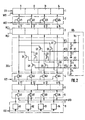
- Redundancy write shift register 1 has four stages 11 to 14 for storing data. At the timing when data is inputted into the stage of a regular write data register (not shown) corresponding to a failed memory cell, data DTI is applied to an input terminal of the register 1. In synchronism with a clock signal WCK, the data DTI is captured and stored in the first place 11. At this time, the register 1 has already been another data, this data is shifted to the next stage. Respective data stored in the stages 11 to 14 are outputted from the respective output nodes thereof.
- a write data transfer circuit 2 includes transistors Q21 to Q24 which are turned on by the active level of a write-data transfer signal WDT.
- the respective data from the stages 11 to 14 of the redundancy write shift register 1 are at the same time (in parallel) transferred to the corresponding memory cell columns 31 to 34 of a redundancy memory cell array 3.
- This redundancy memory cell array 3 is organized of an n rows x 4 columns arrangement (or matrix) of memory cells. Each memory cell columns 31 to 34 contains n memory cells in total. "n" rows are selected by respective word lines WL1 to WLn common to redundancy memory cell array 3 and the regular memory cell array (not shown).
- Each column 31 to 34 of redundancy memory cell array 3 includes totally "n" memory cells per row.
- 4-bit data outputted from the data-transfer path switching circuit 200 are inputted into a read data transfer circuit 4.
- a read data transfer circuit 4 when read-data transfer signal RDT goes active, transistor Q41 to Q44 are turned on to transfer the inputted data to the corresponding stages of a read-data resistor 5 of a redundancy data output circuit.
- the redundancy data output circuit is composed of the read data register 5, an output-data transfer circuit 6, an output bus 7, and an output-control signal generating circuit 8.
- the read data register 5 has four stages 51 to 54. Respective data from transistor Q41 to Q44 of the read data transfer circuit 4 are captured and held in the corresponding stages 51 to 54 of the read data register 5.
- Output-data transfer circuit 6 comprises transistors Q61 to Q64, each being turned on when the corresponding one of output control signals OC1 to OC4 goes active.
- the respective data held in the stages of the read data register 5 are thereby transferred in sequence to the output bus 7 under the control or output control signals OC1 to OC4, and derived as output data DTO.
- Output-control signal generating circuit 8 is composed of decoders 81 to 84, and outputs the control signals OC1 to OC4 which go active in sequence under the timing of read clock signals RCK occuring in synchronism with each data read-out timing from failed memory cells in a normal memory cell array (not shown).
- a data-transfer path switching circuit 200 which responds to switching control signals RC1 to RC4 and changes appropriate one of the data-transfer paths from the memory cell columns 31 to 34 of redundancy memory cell array 3 to the corresponding transistor Q41 to Q44 of read data transfer circuit 4.
- a path-switching-signal generating circuit 100 generates the switching signals RC1 to RC4.
- the circuit 200 includes switching transistors Q1 to Q10 connected as shown.
- j is any integer from 1 ascending to N allocated to the inputs and outputs, respectively, of the data-transfer path switching circuit 200 in sequence from respective one ends (corresponding to memory cell columns 31 to 34 of redundancy memory cell array 3 and to transistor Q41 of data transfer circuit 4), and k is any integer from 1 to N and k ⁇ j allocated to path switching signals, hence designated with RCk.
- Path-switching signal generating circuit 100 consists of resistors R1 to R4 each with one end connected to a common supply voltage Vcc and the other end grounded through a fuse links F1 to F4, and thus is constructed so as to generate path-switching signal RC1 to RC4 from each junction.
- redundancy circuit The operation of the above-described redundancy circuit will be described assuming that there are two failed memory cells (not shown) in one word line (row) in the regular memory cell array (not shown) in the semiconductor memory device.
- the first write data DTI (DTI-1) is, on a write clock signal WCK, input into the redundancy write shift register, and captured and held in the first-place 11 of it.
- the second write data DTI (DTI-2) is, on a write clock signal WCK, input into the redundancy write shift register, and captured and held in the first-place 11 of it.
- the first data DTI-1 is shifted to the second place 12.
- write-data transfer signal WDT goes active.
- data DTI-2 and DTI-1 of places 11, 12 of redundancy write shift register 1 are transferred to, and stored in, the memory cells in memory cell columns 31, 32 selected by one of word lines WL1 to WLn.
- fuse link F2 in the memory device is blown by a known external procedure. Then transistors Q2, Q3 are turned on by path switching signal RC2, and consequently the data of memory cell column 32 in redundancy memory cell array 3 is transferred to the last-place 54 of read data register 5 and the data of memory cell column 31 to the place 53.
- path switching signal RC1 goes to supply voltage level Vcc, which in turn causes transistor Q1 to turn on, and consequently the data of memory cell column 31 in redundancy memory cell array 3 is transferred to the last place 54 of read data register 5 via transistor Q44 of read data transfer circuit 4.
- Other path switching signals RC2 to RC4 remains grounded, that is, at ground potential level through fuse links F2 to F4, respectively, and hence transistors Q2 to Q10 remains off.
- fuse link F3 is blown, with the result that the data of memory cell column 33 is transferred to place 54 of read data register 5, the data of memory cell column 32 to place 53, and the data of memory cell column 31 to place 52.
- fuse link F4 is blown, with the result that the data of memory cell column 34 is transferred to place 54 of read data register 5, and the data of memory cell column 33 to place 53, the data of memory cell column 32 to place 52, and the data of memory cell column 31 to place 51.
- decoders 84, 83, 82 and 81 may be set so that always output control signals OC4, OC3, OC2, and OC1 go active in sequence.
- output-control signal generating circuit 8 at the timing of reading out data DTI-1, that is, the data of the first failed memory cell of the regular memory cell array, output control signal OC4 of active level, on read clock signal RCK, is generated from decoder 84. This signal turns on transistor Q64 of output data transfer circuit 6, and consequently data DTI-1 held in place 54 of read data register 5 is transferred to output bus 7 and output as output data DTO.
- the data of memory cell column 31 of redundancy memory cell array 3 is always transferred to place 51 of read data register 5.
- the data of memory cell column 31 is transferred to, and held in, places 54 and 51 of read data register 5. Since one piece of data only can be read out by read clock signal RCK, however, only the data held in place 54 is read out, and the data held in place 51 is not read out.
- RCK read clock signal
- only the data held in place 54 is read out, and the data held in place 51 is not read out.
- two memory cells are faulty, only respective data held in places 54 and 53 are read out.
- three memory cells are faulty, only respective data held in places 54, 53 and 52 are read out. In the last two cases, the data held in place 51 is not read out.
- respective data of memory cell columns 31, 32, 33 and 34 are transferred to the corresponding places 51, 52, 53 and 54, and these four data are output in the order of from place 54 to place 51.
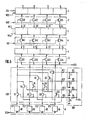
- Fig. 3 is a circuit diagram for illustrating the third embodiment of the present invention involving redundancy circuit.
- This embodiment is distinguished from the first embodiment diagrammed in Fig. 1 in the respect that to respective one ends of resistors R1 to R4 of path-switching signal generating circuit 100a, read data-transfer signal RDT, instead of supply voltage Vcc, is applied thereby to control the timing when path switching signal RC1 to RC4 go to active level.
- data-transfer path switching circuit 200 has additionally the function of read data transfer circuit 5, with an inevitable effect that read data transfer circuit (4 in Fig. 1) can be omitted.
- path switching signal RC1 always goes to supply voltage Vcc level, and hence transistor Q1 is in "on" state at all times.
- read-data transfer signal RDT goes active
- the data of memory cell column 31 is transferred through transistors Q1, Q44 to place 54 of read data register 5.
- path switching signal RC1 goes to active level (supply voltage Vcc level), and in turn transistor Q1 is turned on, consequently the data of memory cell column 31 is transferred through transistor Q1 to place Q54 of read data register 5.
- the third embodiment has advantage of needing four smaller number of transistors as well as the same effect as that of the first embodiment.
- Fig. 4 is a circuit diagram for illustrating the fourth embodiment of the present invention involving redundancy circuit.
- data-transfer path switching circuit 200 is provided between redundancy write shift register 1 and redundancy memory cell array 3. Its basic operation and effects are the same as the first embodiment, and therefore detailed description is omitted.
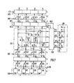
- Fig. 5 is a circuit diagram for illustrating the fifth embodiment of the present invention involving redundancy circuit.
- the output circuit consists of a read shift register 9. Except this respect, the construction is the same as diagrammed in Fig. 1, and therefore the following description will be focused on this output circuit.
- Redundancy read shift register 9 has four places 91 - 94. Once read-data transfer signal RDT goes to active level, respective data of cell columns 31 to 34 of redundency memory cell array 3, under the control read data transfer circuit 4, are transferred through data-path switching circuit 200 to, captured and held in, the corresponding registers 91 to 94. Each time read clock signal RCK goes active, the data held in each place 91 to 94 is shifted over to the next place, and output at the output terminal the last place 94 as output data DTO in bit-serial way.
- the data to be firstly output is transferred to, and held in, the last place 94 of redundancy read shift register 9. Subsequent process is carried out such that in accordance with the number of input data, these data are transferred to, and held in, places 93, 92, 91 in the order of being output.
- read clock signal RCK goes active, in response to which the data held in the last place 94 of the redundancy read shift register 9 is output. Simultaneously with this, respective data held in each place 93, 92, 91 is shifted to the next place, consequently the data to be output in the second turn being held in the last place 94.
- data DTO are output in bit-serial way from the last register cell 94.
- a properly-selected fuse link in path-switching signal generating circuit 100 is blown, thereby the data-transfer path from redundancy memory array 3 to redundancy read shift register 9 being determined by data-transfer path switching circuit 200. Via these determined path, the data are transferred to read shift register 9, and held in places 94, 93, 92 and 91 of it, in the order of being output as the data to be firstly output in the last place 94 and in sequence in accordance with the number of the input data.
- redundancy read shift register 9 When the number of data input into the redundancy circuit, which is the number of failed memory cells in one row of the regular memory cell array is smaller than the number of places of each register, or the like, though needed in the prior art, the procedure is unneeded that any data entered in redundancy read shift register 9 must shifted to the last place 94 previously to being output to the external, with an effect of enabling to speed up data-read speed to the external.
- the fifth embodiment is of redundancy data output circuit consisting of a redundancy read shift register 9. It is as a matter of course that this embodiment may modified by application of not only the constructions of Figs. 2 and 3, but also the construction of Fig. 4 that data-transfer path switching circuit 200 or 200a is provided between redundancy write shift register 1 and redundancy memory cell array 3.
- this redundancy circuit is provided, between output control signal generating circuit 8 and output data transfer circuit of redundancy circuit diagrammed in Fig. 1, with an output control signal path switching circuit 400 for supplying output control signals OC1 to OC4 from output control signal generating circuit 8 to output transistors Q61 to Q64 of data transfer circuit 6 under control, by path switching signals RC1 to RC4, of the switching of respective paths of those output control signals; and a path-switching signal generating circuit 300 for generating path switching signals RC1 to RC4. Accordingly no data-transfer path switching circuit is provided between redundancy memory cell array 3 and read data transfer circuit 4, both being directly connected.
- Output control signal circuit 400 is all the same as data-transfer path switching circuit 200 in the first embodiment except the respect of replacing the input and output by each other.
- Path-switching signal generating circuit 300 is all the same as path switching signal generating circuit 100, too.
- the decoders 84, 83, 82 and 81 have so fixed contents that always output control signals OC4, OC3, OC2 and OC1 are caused to go to active level in the order as mentioned above.
- the procedure of blowing a selected fuse link according to the number of failed memory cells in one row of the regular memory cell array, thus to specify respective paths of output control signals OC1 to OC4, is the same as in the first embodiment.
- the first embodiment is constructed so that switching data-transfer paths from write shift register 1 to redundancy data output circuit can be switched.
- the data-transfer paths are unchanged compared with those in the prior art.
- the paths of output control signals OC1 to OC4 are so switched that the output control signal supplied to the transistor of output data transfer circuit 6 to be firstly turned on is OC4.
- each decoder 81 to 84 in output control signal generating circuit 8 are fixed, paths of output control signal OC1 to OC4 are switched by very simple work of blowing a selected fuse link, thus permitting to minimize risk of mistake in switching work.
- the embodiments diagrammed in Figs. 1 to 6 can be applied as they are when there are found failed memory cell or cells only in one row of the regular memory cell array and when an equal number of failed memory cells are found in a plurality of rows.
- the number of failed memory cells varies from row to row, however, it is difficult to apply these embodiments as they are.
- switch circuit for this case is complicated, too.
- the seventh and eighth embodiments diagrammed in Fig. 7 and 8, respectively, has been developed.
- the redundancy circuit as the seventh embodiment of the present invention is constructed so that a path-switching signal selecting circuit 500 for, when word lines WL1 to WLn is at select level, selecting and supplying one of path switching signals RC1 to RC4 to data-transfer path switching circuit 200 is provided between path-switching signal generating circuit 100 and data-transfer path switching circuit 200.
- Path-switching signal selecting circuit 500 is provided with programmable switch elements for selecting respective path switching signals RC1 to RC4 each being transmitted to respective specified transistor or transistors in data-transfer path switching circuit 200. Turn on or off of each switch element is controlled by the level of the associated word line WL1 to WLn, respectively.
- the program is, for example, written so that assuming if one failed memory cell is found in the corresponding row to a word line WLj and three failed memory cells in the corresponding row to another word line WLk, the active level of word line WLj turns on the switch element for selecting path switching signal RC1 being transmitted to transistor Q1, and the active level of word line WLk turns the switch element on for selecting path switching signal RC3 being transmitted to transistors Q4 to Q6.
- a path-switching signal selecting circuit 500 for selecting one from path switching signals RC1 to RC4 depending on the levels of word lines WL1 to WLn, and aupplying it to output control signal switching circuit 400 between a path-switching signal generating circuit 300 and output control path switching circuit 400 in redundancy circuit of Fig. 6.
- This path control-signal selecting circuit 500 is the same as diagrammed in Fig. 7.
- a path-switching signal selecting circuit 500 of simple design is provided between path-switching signal generating circuit 100 and data-transfer path switching circuit 200 and between path-switching signal generating circuit 300 and output control signal switching circuit 400, respectively, enables easy application in the cases the number of failed memory cells varying with row, as well.
- path-switching signal generating circuit 100 or 300 consists of resistors R1 to R4 and fuse links F1 to F4, and is constructed to, when data-transfer path switching circuit 200, 200 a or output control signal path switching circuit 400 is at active level, turn on suitable one or ones from transistors Q1 to Q10.
- circuit designs are not limitative but any may be used only if it generates path switching signals RC1 to RC4.
Landscapes
- For Increasing The Reliability Of Semiconductor Memories (AREA)
- Dram (AREA)
Applications Claiming Priority (2)
| Application Number | Priority Date | Filing Date | Title |
|---|---|---|---|
| JP14343990 | 1990-06-01 | ||
| JP143439/90 | 1990-06-01 |
Publications (3)
| Publication Number | Publication Date |
|---|---|
| EP0459521A2 true EP0459521A2 (fr) | 1991-12-04 |
| EP0459521A3 EP0459521A3 (en) | 1992-11-19 |
| EP0459521B1 EP0459521B1 (fr) | 1997-03-12 |
Family
ID=15338729
Family Applications (1)
| Application Number | Title | Priority Date | Filing Date |
|---|---|---|---|
| EP91108972A Expired - Lifetime EP0459521B1 (fr) | 1990-06-01 | 1991-05-31 | Dispositif de mémoire à semi-conducteur ayant un circuit de redondance |
Country Status (4)
| Country | Link |
|---|---|
| US (1) | US5255226A (fr) |
| EP (1) | EP0459521B1 (fr) |
| KR (1) | KR950010309B1 (fr) |
| DE (1) | DE69125052T2 (fr) |
Families Citing this family (24)
| Publication number | Priority date | Publication date | Assignee | Title |
|---|---|---|---|---|
| JP2554816B2 (ja) * | 1992-02-20 | 1996-11-20 | 株式会社東芝 | 半導体記憶装置 |
| US5404331A (en) * | 1993-07-30 | 1995-04-04 | Sgs-Thomson Microelectronics, Inc. | Redundancy element check in IC memory without programming substitution of redundant elements |
| JP2776247B2 (ja) * | 1993-11-17 | 1998-07-16 | 日本電気株式会社 | 半導体集積回路及びその製造方法 |
| US5841712A (en) * | 1996-09-30 | 1998-11-24 | Advanced Micro Devices, Inc. | Dual comparator circuit and method for selecting between normal and redundant decode logic in a semiconductor memory device |
| US6629190B2 (en) * | 1998-03-05 | 2003-09-30 | Intel Corporation | Non-redundant nonvolatile memory and method for sequentially accessing the nonvolatile memory using shift registers to selectively bypass individual word lines |
| US6526470B1 (en) * | 1998-09-28 | 2003-02-25 | Cypress Semiconductor Corp. | Fifo bus-sizing, bus-matching datapath architecture |
| US6310880B1 (en) | 2000-03-17 | 2001-10-30 | Silicon Aquarius, Inc. | Content addressable memory cells and systems and devices using the same |
| DE10063684A1 (de) * | 2000-12-20 | 2002-07-18 | Infineon Technologies Ag | Schaltungsanordnung zur Ansteuerung einer programmierbaren Verbindung |
| US20030163769A1 (en) * | 2002-02-27 | 2003-08-28 | Sun Microsystems, Inc. | Memory module including an error detection mechanism for address and control signals |
| US6941493B2 (en) * | 2002-02-27 | 2005-09-06 | Sun Microsystems, Inc. | Memory subsystem including an error detection mechanism for address and control signals |
| US6976194B2 (en) * | 2002-06-28 | 2005-12-13 | Sun Microsystems, Inc. | Memory/Transmission medium failure handling controller and method |
| US6996766B2 (en) * | 2002-06-28 | 2006-02-07 | Sun Microsystems, Inc. | Error detection/correction code which detects and corrects a first failing component and optionally a second failing component |
| US6973613B2 (en) * | 2002-06-28 | 2005-12-06 | Sun Microsystems, Inc. | Error detection/correction code which detects and corrects component failure and which provides single bit error correction subsequent to component failure |
| US7174486B2 (en) * | 2002-11-22 | 2007-02-06 | International Business Machines Corporation | Automation of fuse compression for an ASIC design system |
| US6996686B2 (en) * | 2002-12-23 | 2006-02-07 | Sun Microsystems, Inc. | Memory subsystem including memory modules having multiple banks |
| US7779285B2 (en) * | 2003-02-18 | 2010-08-17 | Oracle America, Inc. | Memory system including independent isolated power for each memory module |
| US7530008B2 (en) | 2003-08-08 | 2009-05-05 | Sun Microsystems, Inc. | Scalable-chip-correct ECC scheme |
| US7188296B1 (en) | 2003-10-30 | 2007-03-06 | Sun Microsystems, Inc. | ECC for component failures using Galois fields |
| JP4732709B2 (ja) * | 2004-05-20 | 2011-07-27 | 株式会社半導体エネルギー研究所 | シフトレジスタ及びそれを用いた電子機器 |
| US7937510B1 (en) * | 2005-02-01 | 2011-05-03 | Altera Corporation | Lempel Ziv compression architecture |
| DE102006022072B4 (de) * | 2005-10-04 | 2008-04-03 | Qimonda Flash Gmbh & Co. Kg | Messschaltung und Leseverfahren für Speicherzellen |
| US8595573B2 (en) * | 2006-12-03 | 2013-11-26 | Apple Inc. | Automatic defect management in memory devices |
| KR101865954B1 (ko) * | 2012-09-21 | 2018-06-08 | 현대자동차주식회사 | 소음 저감을 위한 친환경 자동차의 인버터 제어 방법 |
| CN113569517B (zh) * | 2021-06-29 | 2024-02-23 | 南方电网科学研究院有限责任公司 | 一种减小列冗余替换电路面积的电路及芯片 |
Family Cites Families (3)
| Publication number | Priority date | Publication date | Assignee | Title |
|---|---|---|---|---|
| JPS62152050A (ja) * | 1985-12-26 | 1987-07-07 | Nec Corp | 半導体メモリ |
| US4719601A (en) * | 1986-05-02 | 1988-01-12 | International Business Machine Corporation | Column redundancy for two port random access memory |
| JPH0748316B2 (ja) * | 1988-05-30 | 1995-05-24 | 日本電気株式会社 | デュアルポートメモリ回路 |
-
1991
- 1991-05-31 DE DE69125052T patent/DE69125052T2/de not_active Expired - Fee Related
- 1991-05-31 EP EP91108972A patent/EP0459521B1/fr not_active Expired - Lifetime
- 1991-06-01 KR KR1019910009111A patent/KR950010309B1/ko not_active Expired - Fee Related
- 1991-06-03 US US07/709,565 patent/US5255226A/en not_active Expired - Lifetime
Also Published As
| Publication number | Publication date |
|---|---|
| US5255226A (en) | 1993-10-19 |
| DE69125052T2 (de) | 1997-09-25 |
| KR920001553A (ko) | 1992-01-30 |
| KR950010309B1 (ko) | 1995-09-14 |
| DE69125052D1 (de) | 1997-04-17 |
| EP0459521B1 (fr) | 1997-03-12 |
| EP0459521A3 (en) | 1992-11-19 |
Similar Documents
| Publication | Publication Date | Title |
|---|---|---|
| US5255226A (en) | Semiconductor memory device with a redundancy circuit bypassing failed memory cells | |
| US5394541A (en) | Programmable memory timing method and apparatus for programmably generating generic and then type specific memory timing signals | |
| KR910000737B1 (ko) | 에러 정정기능을 갖추고 있으며 용장 구성을 포함한 반도체 메모리 장치 | |
| KR940006162B1 (ko) | 플래시라이트기능을 구비한 반도체 기억장치 및 그 동작방법 | |
| US5400281A (en) | Static random access memory device with memory cell testing circuit | |
| KR100386442B1 (ko) | 메모리디바이스회로 및 멀티뱅크메모리어레이의 멀티뱅크컬럼의동시어드레스방법 | |
| US5283877A (en) | Single in-line DRAM memory module including a memory controller and cross bar switches | |
| US4483001A (en) | Online realignment of memory faults | |
| EP0029322A1 (fr) | Dispositif de mémoire à semiconducteur avec redondance | |
| JPS62262294A (ja) | メモリ・システム | |
| EP0335125A2 (fr) | Mémoire à accès aléatoire dynamique à redondance et testabilité améliorée | |
| JPS62222500A (ja) | 半導体記憶装置 | |
| GB2235073A (en) | Semiconductor memory device with test circuit | |
| US6202180B1 (en) | Semiconductor memory capable of relieving a defective memory cell by exchanging addresses | |
| KR960011960B1 (ko) | 반도체 기억장치 | |
| KR970003279A (ko) | 메모리회로, 메모리회로의 데이타제어회로 및 메모리회로의 어드레스지정회로 | |
| GB2137784A (en) | Semiconductor memory device with self-correction circuit | |
| JPH03214500A (ja) | メモリ装置 | |
| US3585607A (en) | Memory with redundancy | |
| EP0237030B1 (fr) | Mémoire à semi-conducteurs avec système d'accès sériel rapide | |
| US5367495A (en) | Random access memory having control circuit for maintaining activation of sense amplifier even after non-selection of word line | |
| KR950014901B1 (ko) | 다중 로우 및/또는 컬럼을 가변적으로 선택하는 어드레스 디코더 및 이 디코더를 사용한 반도체 기억 장치 | |
| KR960006284B1 (ko) | 듀얼 포트 반도체 기억장치 | |
| CN100392762C (zh) | 传送地址信息的方法及电路 | |
| US20020118567A1 (en) | Serial storage device |
Legal Events
| Date | Code | Title | Description |
|---|---|---|---|
| PUAI | Public reference made under article 153(3) epc to a published international application that has entered the european phase |
Free format text: ORIGINAL CODE: 0009012 |
|
| 17P | Request for examination filed |
Effective date: 19910531 |
|
| AK | Designated contracting states |
Kind code of ref document: A2 Designated state(s): DE FR GB |
|
| PUAL | Search report despatched |
Free format text: ORIGINAL CODE: 0009013 |
|
| AK | Designated contracting states |
Kind code of ref document: A3 Designated state(s): DE FR GB |
|
| 17Q | First examination report despatched |
Effective date: 19950601 |
|
| GRAG | Despatch of communication of intention to grant |
Free format text: ORIGINAL CODE: EPIDOS AGRA |
|
| GRAH | Despatch of communication of intention to grant a patent |
Free format text: ORIGINAL CODE: EPIDOS IGRA |
|
| GRAH | Despatch of communication of intention to grant a patent |
Free format text: ORIGINAL CODE: EPIDOS IGRA |
|
| GRAA | (expected) grant |
Free format text: ORIGINAL CODE: 0009210 |
|
| AK | Designated contracting states |
Kind code of ref document: B1 Designated state(s): DE FR GB |
|
| PG25 | Lapsed in a contracting state [announced via postgrant information from national office to epo] |
Ref country code: FR Effective date: 19970312 |
|
| REF | Corresponds to: |
Ref document number: 69125052 Country of ref document: DE Date of ref document: 19970417 |
|
| PGFP | Annual fee paid to national office [announced via postgrant information from national office to epo] |
Ref country code: FR Payment date: 19970527 Year of fee payment: 7 |
|
| PG25 | Lapsed in a contracting state [announced via postgrant information from national office to epo] |
Ref country code: GB Free format text: LAPSE BECAUSE OF NON-PAYMENT OF DUE FEES Effective date: 19970612 |
|
| EN | Fr: translation not filed | ||
| PLBE | No opposition filed within time limit |
Free format text: ORIGINAL CODE: 0009261 |
|
| STAA | Information on the status of an ep patent application or granted ep patent |
Free format text: STATUS: NO OPPOSITION FILED WITHIN TIME LIMIT |
|
| GBPC | Gb: european patent ceased through non-payment of renewal fee |
Effective date: 19970612 |
|
| 26N | No opposition filed | ||
| PGFP | Annual fee paid to national office [announced via postgrant information from national office to epo] |
Ref country code: DE Payment date: 20040610 Year of fee payment: 14 |
|
| PG25 | Lapsed in a contracting state [announced via postgrant information from national office to epo] |
Ref country code: DE Free format text: LAPSE BECAUSE OF NON-PAYMENT OF DUE FEES Effective date: 20051201 |