EP0460286A2 - Procédé et arrangement pour le montage d'un composant semi-conducteur avec un substrat ou pour le post-traitement d'une connexion semi-conducteur/substrat par pressage sans contact - Google Patents
Procédé et arrangement pour le montage d'un composant semi-conducteur avec un substrat ou pour le post-traitement d'une connexion semi-conducteur/substrat par pressage sans contact Download PDFInfo
- Publication number
- EP0460286A2 EP0460286A2 EP90123453A EP90123453A EP0460286A2 EP 0460286 A2 EP0460286 A2 EP 0460286A2 EP 90123453 A EP90123453 A EP 90123453A EP 90123453 A EP90123453 A EP 90123453A EP 0460286 A2 EP0460286 A2 EP 0460286A2
- Authority
- EP
- European Patent Office
- Prior art keywords
- semiconductor
- substrate
- plunger
- pressure
- pierced
- Prior art date
- Legal status (The legal status is an assumption and is not a legal conclusion. Google has not performed a legal analysis and makes no representation as to the accuracy of the status listed.)
- Withdrawn
Links
Images

Classifications
-
- H—ELECTRICITY
- H10—SEMICONDUCTOR DEVICES; ELECTRIC SOLID-STATE DEVICES NOT OTHERWISE PROVIDED FOR
- H10P—GENERIC PROCESSES OR APPARATUS FOR THE MANUFACTURE OR TREATMENT OF DEVICES COVERED BY CLASS H10
- H10P72/00—Handling or holding of wafers, substrates or devices during manufacture or treatment thereof
- H10P72/04—Apparatus for manufacture or treatment
- H10P72/0438—Apparatus for making assemblies not otherwise provided for, e.g. package constructions
-
- H—ELECTRICITY
- H10—SEMICONDUCTOR DEVICES; ELECTRIC SOLID-STATE DEVICES NOT OTHERWISE PROVIDED FOR
- H10W—GENERIC PACKAGES, INTERCONNECTIONS, CONNECTORS OR OTHER CONSTRUCTIONAL DETAILS OF DEVICES COVERED BY CLASS H10
- H10W74/00—Encapsulations, e.g. protective coatings
- H10W74/01—Manufacture or treatment
- H10W74/016—Manufacture or treatment using moulds
-
- H—ELECTRICITY
- H10—SEMICONDUCTOR DEVICES; ELECTRIC SOLID-STATE DEVICES NOT OTHERWISE PROVIDED FOR
- H10W—GENERIC PACKAGES, INTERCONNECTIONS, CONNECTORS OR OTHER CONSTRUCTIONAL DETAILS OF DEVICES COVERED BY CLASS H10
- H10W99/00—Subject matter not provided for in other groups of this subclass
-
- H—ELECTRICITY
- H10—SEMICONDUCTOR DEVICES; ELECTRIC SOLID-STATE DEVICES NOT OTHERWISE PROVIDED FOR
- H10W—GENERIC PACKAGES, INTERCONNECTIONS, CONNECTORS OR OTHER CONSTRUCTIONAL DETAILS OF DEVICES COVERED BY CLASS H10
- H10W72/00—Interconnections or connectors in packages
- H10W72/01—Manufacture or treatment
- H10W72/013—Manufacture or treatment of die-attach connectors
- H10W72/01315—Forming coatings
-
- H—ELECTRICITY
- H10—SEMICONDUCTOR DEVICES; ELECTRIC SOLID-STATE DEVICES NOT OTHERWISE PROVIDED FOR
- H10W—GENERIC PACKAGES, INTERCONNECTIONS, CONNECTORS OR OTHER CONSTRUCTIONAL DETAILS OF DEVICES COVERED BY CLASS H10
- H10W72/00—Interconnections or connectors in packages
- H10W72/01—Manufacture or treatment
- H10W72/013—Manufacture or treatment of die-attach connectors
- H10W72/01361—Chemical or physical modification, e.g. by sintering or anodisation
-
- H—ELECTRICITY
- H10—SEMICONDUCTOR DEVICES; ELECTRIC SOLID-STATE DEVICES NOT OTHERWISE PROVIDED FOR
- H10W—GENERIC PACKAGES, INTERCONNECTIONS, CONNECTORS OR OTHER CONSTRUCTIONAL DETAILS OF DEVICES COVERED BY CLASS H10
- H10W72/00—Interconnections or connectors in packages
- H10W72/071—Connecting or disconnecting
- H10W72/0711—Apparatus therefor
- H10W72/07141—Means for applying energy, e.g. ovens or lasers
-
- H—ELECTRICITY
- H10—SEMICONDUCTOR DEVICES; ELECTRIC SOLID-STATE DEVICES NOT OTHERWISE PROVIDED FOR
- H10W—GENERIC PACKAGES, INTERCONNECTIONS, CONNECTORS OR OTHER CONSTRUCTIONAL DETAILS OF DEVICES COVERED BY CLASS H10
- H10W72/00—Interconnections or connectors in packages
- H10W72/071—Connecting or disconnecting
- H10W72/0711—Apparatus therefor
- H10W72/07178—Means for aligning
-
- H—ELECTRICITY
- H10—SEMICONDUCTOR DEVICES; ELECTRIC SOLID-STATE DEVICES NOT OTHERWISE PROVIDED FOR
- H10W—GENERIC PACKAGES, INTERCONNECTIONS, CONNECTORS OR OTHER CONSTRUCTIONAL DETAILS OF DEVICES COVERED BY CLASS H10
- H10W72/00—Interconnections or connectors in packages
- H10W72/071—Connecting or disconnecting
- H10W72/073—Connecting or disconnecting of die-attach connectors
- H10W72/07302—Connecting or disconnecting of die-attach connectors using an auxiliary member
- H10W72/07304—Connecting or disconnecting of die-attach connectors using an auxiliary member the auxiliary member being temporary, e.g. a sacrificial coating
-
- H—ELECTRICITY
- H10—SEMICONDUCTOR DEVICES; ELECTRIC SOLID-STATE DEVICES NOT OTHERWISE PROVIDED FOR
- H10W—GENERIC PACKAGES, INTERCONNECTIONS, CONNECTORS OR OTHER CONSTRUCTIONAL DETAILS OF DEVICES COVERED BY CLASS H10
- H10W72/00—Interconnections or connectors in packages
- H10W72/071—Connecting or disconnecting
- H10W72/073—Connecting or disconnecting of die-attach connectors
- H10W72/07321—Aligning
- H10W72/07327—Aligning involving guiding structures, e.g. spacers or supporting members
-
- H—ELECTRICITY
- H10—SEMICONDUCTOR DEVICES; ELECTRIC SOLID-STATE DEVICES NOT OTHERWISE PROVIDED FOR
- H10W—GENERIC PACKAGES, INTERCONNECTIONS, CONNECTORS OR OTHER CONSTRUCTIONAL DETAILS OF DEVICES COVERED BY CLASS H10
- H10W72/00—Interconnections or connectors in packages
- H10W72/071—Connecting or disconnecting
- H10W72/073—Connecting or disconnecting of die-attach connectors
- H10W72/07331—Connecting techniques
- H10W72/07336—Soldering or alloying
-
- H—ELECTRICITY
- H10—SEMICONDUCTOR DEVICES; ELECTRIC SOLID-STATE DEVICES NOT OTHERWISE PROVIDED FOR
- H10W—GENERIC PACKAGES, INTERCONNECTIONS, CONNECTORS OR OTHER CONSTRUCTIONAL DETAILS OF DEVICES COVERED BY CLASS H10
- H10W72/00—Interconnections or connectors in packages
- H10W72/071—Connecting or disconnecting
- H10W72/073—Connecting or disconnecting of die-attach connectors
- H10W72/07331—Connecting techniques
- H10W72/07337—Connecting techniques using a polymer adhesive, e.g. an adhesive based on silicone or epoxy
-
- H—ELECTRICITY
- H10—SEMICONDUCTOR DEVICES; ELECTRIC SOLID-STATE DEVICES NOT OTHERWISE PROVIDED FOR
- H10W—GENERIC PACKAGES, INTERCONNECTIONS, CONNECTORS OR OTHER CONSTRUCTIONAL DETAILS OF DEVICES COVERED BY CLASS H10
- H10W72/00—Interconnections or connectors in packages
- H10W72/30—Die-attach connectors
- H10W72/321—Structures or relative sizes of die-attach connectors
- H10W72/325—Die-attach connectors having a filler embedded in a matrix
-
- H—ELECTRICITY
- H10—SEMICONDUCTOR DEVICES; ELECTRIC SOLID-STATE DEVICES NOT OTHERWISE PROVIDED FOR
- H10W—GENERIC PACKAGES, INTERCONNECTIONS, CONNECTORS OR OTHER CONSTRUCTIONAL DETAILS OF DEVICES COVERED BY CLASS H10
- H10W72/00—Interconnections or connectors in packages
- H10W72/30—Die-attach connectors
- H10W72/351—Materials of die-attach connectors
- H10W72/352—Materials of die-attach connectors comprising metals or metalloids, e.g. solders
Definitions
- the invention relates to methods for connecting a semiconductor to a substrate or for the aftertreatment of a semiconductor / substrate connection by pressing, and to arrangements for carrying them out.
- connection technologies such as gluing or soldering are used for this, which can be carried out quickly, cheaply and fully automatically.
- the temperature resistance and the temperature change resistance are limited.
- the thermal and electrical resistance of the adhesive also has a disadvantageous effect.
- a high-strength connection can be achieved with low thermal and electrical resistance by pressure sintering a silver powder layer according to EP-A-242 626.
- a pressure is applied to the parts to be connected by rigid stamps.
- the top of the semiconductor is completely touched in this pressing process by a pressure-transmitting solid medium.
- EP-330 896 and EP-330 895 it is also known to embed the substrate and the semiconductor in an elastic centering mold, for example made of silicone rubber, which transmits the pressing pressure of a movable stamp by the remaining interior space when the sintering pressure is reached one Filling chamber completely, in which the substrate and the semiconductor body are located.
- an elastic centering mold for example made of silicone rubber
- the invention has for its object to provide methods of the type mentioned, in which semiconductors are advantageously connected to substrates by pressing or pre-connected semiconductor / substrate connections are advantageously treated by pressing. This is achieved according to the invention by designing the method according to the characterizing parts of patent claims 1 or 2.
- Claims 3 to 12 and 15 to 17 are directed to advantageous developments of the method according to the invention.
- Claims 13 and 14 relate to advantageous arrangements for carrying out the method according to claims 10 or 11.
- Claim 18 is directed to an advantageous arrangement for carrying out the method according to claim 15.
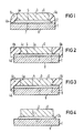
- the intermediate layer 2 lies between the semiconductor surface 5 and the substrate surface 7, which are optionally pretreated, and itself consists of a thermally and electrically highly conductive powder, for example silver powder, which is present, for example, as a pre-sintered film.
- the lateral edge surface 4a of the semiconductor 3 is bonded and sealed to an annular outer region 4b of the substrate surface 7 by an annular, elastic bead 6a, for example a silicone bead.
- an annular edge passivation 6b of a semiconductor 3a shown in FIG. 2 can be used.
- the edge passivation 6b consists of a soft and elastic plastic, for example silicone, and is shaped in such a way that the side edge surface 4c of the semiconductor 3a, which has an indentation for better fastening, is connected and sealed to a region 4d of the side edge surface of the substrate 1 .
- a ring 6c preformed from a soft and elastic plastic, for example silicone, shown in FIG. 3 can be used.
- the plastic ring 6c can either be applied to the intermediate layer 2 after the semiconductor 2 has been applied or applied together with the semiconductor 3. If the plastic ring 6c is applied, it must seal the area between the lateral edge surface 4a of the semiconductor 3 and the area 4d of the lateral edge surface of the substrate.
- an autoclave is a heatable pressure vessel, which in this case must be designed for a pressure of 300 to 400 bar and is best to have an internal heater.
- Systems for hot isostatic pressing (HIP) are particularly suitable for this.
- the pressing pressure of a chemically inert and non-solid medium located in the autoclave causes compressive forces on a surface O of the semiconductors 3 or 3a and on a surface 8 of the respective substrate 1.
- the seals 6a, 6b or 6c prevent a back pressure from building up in the intermediate layer 2; no counterforces can thus be brought about on the surfaces 5, 7 and as a result the arrangement of semiconductor, intermediate layer and substrate is pressed together.
- the intermediate layer 2 is strongly compressed by the pressure and a connection is created by pressure sintering.
- an intermediate layer 2 is dispensed with and only the optionally pretreated semiconductor surface 5 and optionally pretreated substrate surface 7 are pressed onto one another, a connection is formed in a corresponding manner by diffusion welding.
- the surfaces 5, 7 can be pretreated here, for example, by galvanic application or vapor deposition of a noble metal contacting layer.
- a pre-bonded semiconductor / substrate connection shown in FIG. 4 can be post-sintered to increase the bond strength with the help of post-treatment by contact-free pressing and at a suitable temperature.
- the semiconductor / substrate connection is also pre-connected, for example, by contact-free pressing.
- a seal between semiconductor 3 and substrate 1 is not necessary, in particular in the case of power semiconductors, since the penetration speed, even in the case of a gaseous pressure medium, is so low in the compressed intermediate layer 2a, for example consisting of silver powder, that in the case of semiconductor components, such as, for example, power semiconductor components, pressure equalization only occurs after many minutes.
- pressing takes place in an autoclave.
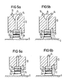
- the first method according to the invention can also be carried out by an arrangement described in FIG. 5a or FIG. 5b.
- the semiconductor 3b or 3 is located on a heating block 9 for heating.
- the semiconductor 3b has a slightly raised, annular outer region 10a, on which a pierced plunger 11a lies without a raised outer region.
- the outside area can consist of silicone lacquer, for example.
- a pierced plunger 11b has a slightly raised annular outer region and the semiconductor 3 has no corresponding outer region for this.
- the semiconductors 3b and 3 can be coated with a sinterable intermediate layer 2b, for example a silver sponge, during the connection by pressure sintering.
- the pierced plungers 11a and 11b each have a bore 12 which connects an inner region 17, which is enclosed in a ring by the associated outer region 10a or 10b, with the cylinder interior 18 of a cylinder 13.
- a three-way valve 15 enables an optional connection between the cylinder interior 18 and an inlet 14 or an outlet 16.
- the substrate 1 is preheated on the heating block 9, the pierced plunger 11a or 11b is placed on the semiconductor 3b or 3 such that a seal between the pierced plunger 11a or 11b and the semiconductor 3b or 3rd is effected. If the outlet 16 is now connected to the cylinder interior 18 by the three-way valve 15, the cylinder interior 18 and, via the bore 12, also the inner region 17 are evacuated, which causes the semiconductor 3b or 3 to be sucked in.
- the semiconductor 3b or 3 can now, together with the plunger 11a or 11b and the cylinder 13, be positioned exactly on the substrate 1 before the inlet 14 is connected to the cylinder interior 18 with the help of the three-way valve 15 and the pressing pressure of the chemically inert and non-solid medium, for example nitrogen or argon as a gaseous and silicone oil as a liquid medium, builds up in the interior 17 between the plunger and the semiconductor and presses the latter onto the preheated substrate 1 without contact.
- the chemically inert and non-solid medium for example nitrogen or argon as a gaseous and silicone oil as a liquid medium
- the arrangement for carrying out the second method according to the invention has a direct connection between the inlet 14 for the chemically inert and non-solid medium and the cylinder interior 18, since suction is carried out when the second method according to the invention is carried out for exact positioning, because the substrate 1 is already connected to the semiconductor 3b or 3 directly or through the pre-compressed intermediate layer 2a to form a semiconductor / substrate connection.
- the plastic melt required for their production for example a thermosetting synthetic resin composition
- the plastic melt required for their production can simultaneously be used as a chemically inert and non-solid medium for the first or second method according to the invention. This is possible because the encapsulation takes place at temperatures around 200 ° C and a pressure of several hundred bar with a holding time of a few minutes.
- FIG. 7 shows an arrangement for carrying out the first or second method according to the invention, in which the injection pressure of a plastic melt for connecting the semiconductors 3c and 3d to the substrates 1b and 1a through an intermediate layer 2 or for post-treating the already existing semiconductor / substrate connections 3c, 1b and 3d, 1a.
- the arrangement shown in FIG. 7 is used in particular for the production of semiconductor modules and essentially consists of an upper injection mold 23 and a lower injection mold 24, which together form an injection chamber 27, an injection channel 25 for supplying the plastic melt and a thin ventilation channel 26.
- the plastic melt under the injection pressure penetrates through the injection channel 25 into the injection chamber 27, flows around the parts located in the injection chamber and exerts a hydrostatic pressure without, however, because of their high level Viscosity penetrate into the intermediate layer 2 and build up a back pressure.
- FIG. 8 shows a further arrangement for carrying out the first or second method according to the invention, in which the injection pressure of a plastic melt for connecting a semiconductor 3e to a substrate 1c through an intermediate layer or for post-treating the already existing semiconductor / substrate connection 3e, 1c.
- the arrangement shown in FIG. 8 is used in particular for the production of semiconductor components with a wafer housing and essentially consists of an upper injection mold 23a, an intermediate mold 31 and a lower injection mold 24a, which together form an injection chamber 27a.
- the spray chamber 27a is connected via a spray channel 25a to a press chamber 29 which has a press piston 30.
- the spray chamber 27a since the spray chamber 27a only surrounds the arrangement of an upper contact piece 32, the semiconductor 3e, the substrate 1c and a lower contact piece 33, no pressing forces can be exerted on the contact pieces 32, 33 by the plastic melt of the spray chamber.
- an additional chamber 28 connected to the pressing chamber 29 via an additional injection channel 25b.
- the connection of the additional chamber to the press chamber could also be formed indirectly, for example by an additional spray channel between the additional chamber and the spray chamber. If, for example, an additional chamber is not sufficient in a special semiconductor / substrate arrangement, a plurality of additional chambers connected directly or indirectly to the press chamber can be provided.
- the spray chamber 27a has a thin ventilation channel 26a and the additional chamber 28 has a thin additional ventilation channel 26b, both ventilation channels 26a, 26b having to be so thin that the plastic melt cannot escape.
- the arrangement of the upper contact piece 32, the semiconductor 3e, the substrate 1c and the lower contact piece 33 is introduced into the lower injection mold 24a, and then the Intermediate mold 31 placed and the injection mold closed by the upper injection mold 23a.
- the press chamber is then filled with the plastic to be sprayed and the melt is injected into the mold. After the plastic melt has hardened, the injection mold is opened, the plastic material of the additional chamber is removed from the component and the finished component is removed from the injection mold.
- a press chamber can simultaneously supply several injection molds with the plastic melt, so that several components can be encapsulated in one operation.
- the first and second methods according to the invention are primarily intended for the processing of entire semiconductor wafers, but can also be applied to semiconductor chips without problems.
Landscapes
- Encapsulation Of And Coatings For Semiconductor Or Solid State Devices (AREA)
- Wire Bonding (AREA)
- Die Bonding (AREA)
Applications Claiming Priority (2)
| Application Number | Priority Date | Filing Date | Title |
|---|---|---|---|
| DE4018131 | 1990-06-06 | ||
| DE4018131 | 1990-06-06 |
Publications (2)
| Publication Number | Publication Date |
|---|---|
| EP0460286A2 true EP0460286A2 (fr) | 1991-12-11 |
| EP0460286A3 EP0460286A3 (en) | 1992-02-26 |
Family
ID=6407893
Family Applications (1)
| Application Number | Title | Priority Date | Filing Date |
|---|---|---|---|
| EP19900123453 Withdrawn EP0460286A3 (en) | 1990-06-06 | 1990-12-06 | Method and arrangement for bonding a semiconductor component to a substrate or for finishing a semiconductor/substrate connection by contactless pressing |
Country Status (3)
| Country | Link |
|---|---|
| US (1) | US5158226A (fr) |
| EP (1) | EP0460286A3 (fr) |
| JP (1) | JPH0529362A (fr) |
Cited By (6)
| Publication number | Priority date | Publication date | Assignee | Title |
|---|---|---|---|---|
| EP1280196A1 (fr) * | 2001-07-18 | 2003-01-29 | Abb Research Ltd. | Procédé de fixatoin de dispositifs électroniques sur des substrats |
| DE102007022338A1 (de) * | 2007-07-26 | 2009-04-09 | Semikron Elektronik Gmbh & Co. Kg | Leistungshalbleiterbauelement mit Metallkontaktschicht sowie Herstellungsverfahren hierzu |
| DE102011080929A1 (de) * | 2011-08-12 | 2013-02-14 | Infineon Technologies Ag | Verfahren zur Herstellung eines Verbundes und eines Leistungshalbleitermoduls |
| EP2390904A3 (fr) * | 2010-05-27 | 2014-03-26 | SEMIKRON Elektronik GmbH & Co. KG | Procédé d'interconnexion de pression à basse température de deux partenaires de liaison et agencement ainsi fabriqué |
| DE102017216545A1 (de) | 2017-09-19 | 2018-11-29 | Conti Temic Microelectronic Gmbh | Vorrichtung und Verfahren zur Herstellung einer Niedertemperatur-Drucksinterverbindung für eine elektronische Baugruppe |
| DE102023201314A1 (de) * | 2023-02-16 | 2024-08-22 | Zf Friedrichshafen Ag | Verfahren zum Verbinden von zumindest einem Bauteil mit zumindest einem Substrat |
Families Citing this family (12)
| Publication number | Priority date | Publication date | Assignee | Title |
|---|---|---|---|---|
| DE4233073A1 (de) * | 1992-10-01 | 1994-04-07 | Siemens Ag | Verfahren zum Herstellen eines Halbleiter-Modulaufbaus |
| DE4315272A1 (de) * | 1993-05-07 | 1994-11-10 | Siemens Ag | Leistungshalbleiterbauelement mit Pufferschicht |
| US5632434A (en) * | 1995-06-29 | 1997-05-27 | Regents Of The University Of California | Pressure activated diaphragm bonder |
| JP3491481B2 (ja) * | 1996-08-20 | 2004-01-26 | 株式会社日立製作所 | 半導体装置とその製造方法 |
| FR2915622B1 (fr) * | 2007-04-30 | 2009-07-31 | Valeo Electronique Sys Liaison | Procde d'assemblage d'un organe sur un support par frittage d'une masse de poudre conductrice |
| DE102008009510B3 (de) * | 2008-02-15 | 2009-07-16 | Danfoss Silicon Power Gmbh | Verfahren zum Niedertemperatur-Drucksintern |
| JP5830847B2 (ja) * | 2010-10-21 | 2015-12-09 | 富士通株式会社 | 半導体装置の製造方法及び接合方法 |
| TWM450049U (zh) * | 2012-11-20 | 2013-04-01 | 印能科技有限公司 | 具有延伸連通腔道結構之半導體封裝載熱裝置 |
| US20140224409A1 (en) * | 2013-02-11 | 2014-08-14 | International Rectifier Corporation | Sintering Utilizing Non-Mechanical Pressure |
| JP2015115481A (ja) * | 2013-12-12 | 2015-06-22 | 株式会社東芝 | 半導体部品および半導体部品の製造方法 |
| CN105234547A (zh) * | 2015-10-20 | 2016-01-13 | 兰微悦美(天津)科技有限公司 | 互不固溶金属的连接工艺 |
| DE102020114442A1 (de) * | 2020-05-29 | 2021-12-02 | Danfoss Silicon Power Gmbh | Halbleiterbauelement |
Family Cites Families (9)
| Publication number | Priority date | Publication date | Assignee | Title |
|---|---|---|---|---|
| US3608809A (en) * | 1968-08-16 | 1971-09-28 | Western Electric Co | Apparatus for uniform multiple-lead bonding |
| US3699640A (en) * | 1970-12-01 | 1972-10-24 | Western Electric Co | Compliant bonding |
| US3964666A (en) * | 1975-03-31 | 1976-06-22 | Western Electric Company, Inc. | Bonding contact members to circuit boards |
| US4159921A (en) * | 1975-08-06 | 1979-07-03 | Sharp Kabushiki Kaisha | Method of connecting an element having multiple terminals and a multi-lead flexible connector |
| US4638937A (en) * | 1985-04-22 | 1987-01-27 | Gte Communication Systems Corporation | Beam lead bonding apparatus |
| IN168174B (fr) * | 1986-04-22 | 1991-02-16 | Siemens Ag | |
| DE3777522D1 (de) * | 1986-10-17 | 1992-04-23 | Hitachi Ltd | Verfahren zum herstellen einer gemischten struktur fuer halbleiteranordnung. |
| EP0330895B1 (fr) * | 1988-03-03 | 1994-12-14 | Siemens Aktiengesellschaft | Procédé pour fixer des composants électroniques sur des substrats et dispositif pour sa réalisation |
| EP0330896A3 (fr) * | 1988-03-03 | 1991-01-09 | Siemens Aktiengesellschaft | Procédé pour fixer des composants semi-conducteurs sur des substrats et dispositifs pour sa réalisation |
-
1990
- 1990-12-06 EP EP19900123453 patent/EP0460286A3/de not_active Withdrawn
-
1991
- 1991-01-22 US US07/643,507 patent/US5158226A/en not_active Expired - Fee Related
- 1991-06-03 JP JP3159777A patent/JPH0529362A/ja not_active Withdrawn
Cited By (10)
| Publication number | Priority date | Publication date | Assignee | Title |
|---|---|---|---|---|
| EP1280196A1 (fr) * | 2001-07-18 | 2003-01-29 | Abb Research Ltd. | Procédé de fixatoin de dispositifs électroniques sur des substrats |
| US6935556B2 (en) | 2001-07-18 | 2005-08-30 | Abb Research Ltd. | Method for mounting electronic components on substrates |
| DE102007022338A1 (de) * | 2007-07-26 | 2009-04-09 | Semikron Elektronik Gmbh & Co. Kg | Leistungshalbleiterbauelement mit Metallkontaktschicht sowie Herstellungsverfahren hierzu |
| US8110925B2 (en) | 2007-07-26 | 2012-02-07 | Semikron Elektronik Gmbh & Co., Kg | Power semiconductor component with metal contact layer and production method therefor |
| DE102007022338B4 (de) * | 2007-07-26 | 2013-12-05 | Semikron Elektronik Gmbh & Co. Kg | Herstellungsverfahren für ein Leistungshalbleiterbauelement mit Metallkontaktschicht |
| EP2390904A3 (fr) * | 2010-05-27 | 2014-03-26 | SEMIKRON Elektronik GmbH & Co. KG | Procédé d'interconnexion de pression à basse température de deux partenaires de liaison et agencement ainsi fabriqué |
| DE102011080929A1 (de) * | 2011-08-12 | 2013-02-14 | Infineon Technologies Ag | Verfahren zur Herstellung eines Verbundes und eines Leistungshalbleitermoduls |
| DE102011080929B4 (de) * | 2011-08-12 | 2014-07-17 | Infineon Technologies Ag | Verfahren zur Herstellung eines Verbundes und eines Leistungshalbleitermoduls |
| DE102017216545A1 (de) | 2017-09-19 | 2018-11-29 | Conti Temic Microelectronic Gmbh | Vorrichtung und Verfahren zur Herstellung einer Niedertemperatur-Drucksinterverbindung für eine elektronische Baugruppe |
| DE102023201314A1 (de) * | 2023-02-16 | 2024-08-22 | Zf Friedrichshafen Ag | Verfahren zum Verbinden von zumindest einem Bauteil mit zumindest einem Substrat |
Also Published As
| Publication number | Publication date |
|---|---|
| US5158226A (en) | 1992-10-27 |
| JPH0529362A (ja) | 1993-02-05 |
| EP0460286A3 (en) | 1992-02-26 |
Similar Documents
| Publication | Publication Date | Title |
|---|---|---|
| EP0460286A2 (fr) | Procédé et arrangement pour le montage d'un composant semi-conducteur avec un substrat ou pour le post-traitement d'une connexion semi-conducteur/substrat par pressage sans contact | |
| EP0330895B1 (fr) | Procédé pour fixer des composants électroniques sur des substrats et dispositif pour sa réalisation | |
| EP3103138B1 (fr) | Procédé de montage d'un composant électrique en utilisant un capot | |
| DE102011080929B4 (de) | Verfahren zur Herstellung eines Verbundes und eines Leistungshalbleitermoduls | |
| EP1796137B1 (fr) | Appareil et méthode cadencée pour frittage sous pression | |
| EP1030349B1 (fr) | Méthode et dispositif pour le traitement de composants électroniques montés sur substrat, en particulier de puces semi-conductrices | |
| EP0330896A2 (fr) | Procédé pour fixer des composants semi-conducteurs sur des substrats et dispositifs pour sa réalisation | |
| EP2179443A1 (fr) | Module et fabrication d'un tel module | |
| EP3105784A1 (fr) | Procédé de montage d'un composant électrique en utilisant un capot et capot adapté pour être employé dans ce procédé | |
| EP4416758B1 (fr) | Dispositif de brasage par diffusion et/ou dispositif de frittage, outil et installation permettant de relier des composants d'au moins un module électronique | |
| DE102014114093A1 (de) | Verfahren und Vorrichtung zum Niedertemperatur-Drucksintern | |
| DE2702623A1 (de) | Druckplatte fuer eine schallplattenpresse, einrichtung zur herstellung von schallplatten sowie schallplattenpresse mit einer druckplatte | |
| EP1894717A1 (fr) | Presse et procédé pour laminer à chaud et sous pression des objets en forme de plaques | |
| WO2017137420A2 (fr) | Dispositif de frittage | |
| EP3618993A1 (fr) | Dispositif de brasage et procédé pour réaliser une liaison brasée entre des éléments par utilisation d'un matériau adhésif pour la liaison provisoire entre les éléments | |
| EP1766674B1 (fr) | Procédé et dispositif permettant la mise en contact mutuel de deux plaquettes | |
| DE102018110132B3 (de) | Drucksinterverfahren bei dem Leistungshalbleiterbauelemente mit einem Substrat über eine Sinterverbindung miteinander verbunden werden | |
| EP3618994A1 (fr) | Dispositif de brasage et procédé pour réaliser une liaison brasée par utilisation d'une plaque de base et d'une plaque de pression et d'un dispositif de butée | |
| DE102007022338B4 (de) | Herstellungsverfahren für ein Leistungshalbleiterbauelement mit Metallkontaktschicht | |
| WO2009000682A1 (fr) | Dispositif de pressage de puces semi-conductrices | |
| DE102015108512B4 (de) | Verfahren zur Herstellung einer stoffschlüssigen Verbindung und Bestückungsautomat | |
| WO2025125195A1 (fr) | Film composite de distribution de pression et procédé de distribution de force de pression dans un processus de frittage | |
| DE2535383C2 (de) | Verfahren zum Herstellen eines Schichtkörpers und für das Verfahren geeignetes Preßblech | |
| WO1999005718A2 (fr) | Pastille de matiere ainsi que procede pour la fabrication d'un corps composite en plastique | |
| DE102004010399A1 (de) | Vorrichtung zum thermischen Verbinden von Elementen mit einem Substrat |
Legal Events
| Date | Code | Title | Description |
|---|---|---|---|
| PUAI | Public reference made under article 153(3) epc to a published international application that has entered the european phase |
Free format text: ORIGINAL CODE: 0009012 |
|
| 17P | Request for examination filed |
Effective date: 19901220 |
|
| AK | Designated contracting states |
Kind code of ref document: A2 Designated state(s): CH DE FR GB IT LI SE |
|
| PUAL | Search report despatched |
Free format text: ORIGINAL CODE: 0009013 |
|
| AK | Designated contracting states |
Kind code of ref document: A3 Designated state(s): CH DE FR GB IT LI SE |
|
| 17Q | First examination report despatched |
Effective date: 19940308 |
|
| STAA | Information on the status of an ep patent application or granted ep patent |
Free format text: STATUS: THE APPLICATION IS DEEMED TO BE WITHDRAWN |
|
| 18D | Application deemed to be withdrawn |
Effective date: 19951228 |