EP0460885B1 - Berührungsloser IC-Aufzeichnungsträger - Google Patents
Berührungsloser IC-Aufzeichnungsträger Download PDFInfo
- Publication number
- EP0460885B1 EP0460885B1 EP91304982A EP91304982A EP0460885B1 EP 0460885 B1 EP0460885 B1 EP 0460885B1 EP 91304982 A EP91304982 A EP 91304982A EP 91304982 A EP91304982 A EP 91304982A EP 0460885 B1 EP0460885 B1 EP 0460885B1
- Authority
- EP
- European Patent Office
- Prior art keywords
- clock
- transfer information
- writer
- reader
- transfer
- Prior art date
- Legal status (The legal status is an assumption and is not a legal conclusion. Google has not performed a legal analysis and makes no representation as to the accuracy of the status listed.)
- Expired - Lifetime
Links
Images


Classifications
-
- G—PHYSICS
- G06—COMPUTING OR CALCULATING; COUNTING
- G06K—GRAPHICAL DATA READING; PRESENTATION OF DATA; RECORD CARRIERS; HANDLING RECORD CARRIERS
- G06K7/00—Methods or arrangements for sensing record carriers, e.g. for reading patterns
- G06K7/10—Methods or arrangements for sensing record carriers, e.g. for reading patterns by electromagnetic radiation, e.g. optical sensing; by corpuscular radiation
- G06K7/10009—Methods or arrangements for sensing record carriers, e.g. for reading patterns by electromagnetic radiation, e.g. optical sensing; by corpuscular radiation sensing by radiation using wavelengths larger than 0.1 mm, e.g. radio-waves or microwaves
- G06K7/10316—Methods or arrangements for sensing record carriers, e.g. for reading patterns by electromagnetic radiation, e.g. optical sensing; by corpuscular radiation sensing by radiation using wavelengths larger than 0.1 mm, e.g. radio-waves or microwaves using at least one antenna particularly designed for interrogating the wireless record carriers
- G06K7/10336—Methods or arrangements for sensing record carriers, e.g. for reading patterns by electromagnetic radiation, e.g. optical sensing; by corpuscular radiation sensing by radiation using wavelengths larger than 0.1 mm, e.g. radio-waves or microwaves using at least one antenna particularly designed for interrogating the wireless record carriers the antenna being of the near field type, inductive coil
-
- G—PHYSICS
- G06—COMPUTING OR CALCULATING; COUNTING
- G06K—GRAPHICAL DATA READING; PRESENTATION OF DATA; RECORD CARRIERS; HANDLING RECORD CARRIERS
- G06K19/00—Record carriers for use with machines and with at least a part designed to carry digital markings
- G06K19/06—Record carriers for use with machines and with at least a part designed to carry digital markings characterised by the kind of the digital marking, e.g. shape, nature, code
- G06K19/067—Record carriers with conductive marks, printed circuits or semiconductor circuit elements, e.g. credit or identity cards also with resonating or responding marks without active components
- G06K19/07—Record carriers with conductive marks, printed circuits or semiconductor circuit elements, e.g. credit or identity cards also with resonating or responding marks without active components with integrated circuit chips
- G06K19/0723—Record carriers with conductive marks, printed circuits or semiconductor circuit elements, e.g. credit or identity cards also with resonating or responding marks without active components with integrated circuit chips the record carrier comprising an arrangement for non-contact communication, e.g. wireless communication circuits on transponder cards, non-contact smart cards or RFIDs
Definitions
- the present invention relates to a card-shaped or coin-shaped IC recording medium, particularly to non-contact IC recording medium provided with a receiving coil and a transmission coil, in which when mounted in a reader/writer, these coils are magnetically connected with the corresponding coils of the reader/writer so that a non-contact data transmission/reception paths are formed between the recording medium and the reader/writer.
- an IC card incorporating an IC circuit such as a memory to store large capacity data.
- the IC card is mounted in a reader/writer. Then, the electric contact on the IC card is brought into contact with that of the reader/writer so that the IC card is electrically connected with the reader/writer.
- the electric contact is attached to the IC card so that it is exposed externally. And also, usually such an IC card is always carried with a user so that dust is likely to be stuck to the electric contact or static electricity is likely to be generated there. If dust is stucked to the electric contact, contact state between the respective electric contacts of the IC card and the reader/writer will become poor. If static electricity is generated at the electric contact of the IC card, a high voltage will be applied to the IC module within the IC card so that IC module may be destroyed.
- a means of connecting an IC card with a reader/writer through magnetic coupling has been proposed.
- This is referred to as a non-contact IC card.
- a card body is provided with coils for data transmission and data reception whereas a reader/writer is also provided with the corresponding coils for data transmission and data reception.
- the non-contact IC card is mounted in the reader/writer, the corresponding coils are magnetically coupled with each other to form two-route data transfer paths having different directions.
- the data transfer paths are formed in a non-contact manner through magnetic coupling so that the above problem attendant on an IC card provided with an electric contact does not arise.
- a clock is required.
- the clock is supplied from the reader/writer to the IC card. Therefore, in the non-contact IC card, it can be proposed to supply the clock from the reader/writer. However, this requires undesired provision of a coil for clock transfer.
- the reader/writer includes a quartz oscillator which is very stable as the clock generating means. Therefore, in order for the non-contact IC card to process the data transferred from the reader/writer at such a stable transfer rate and also transfer the processed data to the reader/writer, the clock generating means to be incorporated in the non-contact IC card must be a quartz oscillator which is stable and can generate the clock at the frequency which is exactly equal to that of the clock in the reader/writer. However, it is very difficult to locate the quartz oscillator, which has a comparatively large size and thickness, within a limited inner space of the non-contact IC card.
- An object of the present invention is to solve the problem described above and to provide IC recording medium which can use a means of generating a clock at the frequency different from that of the clock in a reader/writer.
- a non-contact IC recording medium having a receiving coil and a transmission coil and a signal processing circuit which outputs, in data transmission, data at least provided with a start bit and a stop bit for every m items as transfer information, where m is an integer ⁇ 2, wherein in data transmission and reception, a synchronisation (sync) signal is received from a reader/writer through the receiving coil, the IC recording medium comprising:
- the second clock has the frequency higher than the first clock.
- the m number of items of transfer information output from the signal processing circuit are in synchronism with the second clock. If the third means writes them using the second clock and reads out them using the first clock, the m number of transfer information read out will become synchronous with the first clock so that the reader/writer can take in the transfer information. Thus, the baud rate of the transfer information will be converted so that the information can be taken in the reader/writer by the third means.
- the frequency of the clock used in the non-contact IC recording medium may be different from the clock frequency in the reader/writer and may be varied. Therefore, the clock generating means for the non-contact IC recording medium may be constituted by an oscillator such as a CR oscillator and a ringing oscillator which can be small-sized and thin unlike the quartz oscillator.
- the subsequent m number of items of information are placed in a wait condition by the fourth means, and their wait condition is released by the fifth means to sent them number of items of information to the third means.
- Non-contact IC recording medium having a receiving coil, a transmission coil and a signal processing circuit, which serve to execute signal transmission and reception in a start-stop synchronisation manner, wherein in data transmission and reception, a sync signal is received through said receiving coil, comprising:
- Yet another aspect of the invention provides a non-contact IC recording medium comprising:
- the non-contact IC recording medium in the present invention refers to a recording medium designed in a portable shape such as a card, a coin and a key which can transmit/receive data through magnetic coupling, store the received data in an incorporated memory such an EEPROM located in the recording medium by means of CPU also located within the recording medium, and transmit the data stored in the incorporated memory to a reader/writer through CPU.
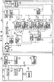
- Figure 1A is a block diagram of one embodiment of the IC card according to the present invention.
- Such a state permits data communication to be performed between the non-contact IC card and the reader/writer.
- the data communication is usually executed in a start-stop synchronization system.
- the data format in the data communication in the start-stop synchronous system is composed of 11 bits consisting of 1 start bit, 8 data bits, 1 parity bit and 1 stop bit. This information composed of 11 bits will be referred to as transfer information.
- the data are usually transferred at the transfer rate (baud rate) of 9600 (bps).
- the transfer information will be transferred with an amplitude-modulated carrier wave for example.
- the modulated transfer information sent through the coil 6 is received by the receiving circuit 4 and is subjected to processing such as demodulation.
- the transfer information (a) from the receiving circuit 4 is alternately distributed to the shift registers 8 and 9 by the switch 7. Specifically, the switch 7 selects the shift register 8 to which one item of the information (a) is to be sent, and thereafter the switch 7 selects the shift register 9 for which the subsequent item of the transfer information (a).
- the sync signal separating circuit 5 separates the sync signal from the received transfer information to produce a shift clock (b) in phase with each of the bits of the transfer information.
- This in-phase signal can be detected in terms of e.g. the edge of the start bit of the demodulated transfer information.
- the shift clock (b) will be produced on the basis of this edge detection timing at the period defined by the above transfer rate of 9600 (bps).
- the selecting circuit 11 when the transfer information (a) is supplied to the shift register 8 by the switch 7, selects the shift clock (b). Then, each bit of the transfer information is successively transferred into the shift register 8 by the shift clock (b). Thus, the transfer information (a) is stored there.
- the selecting circuit 12 when the transfer information (a) is supplied to the shift register 9 by the switch 7, selects the shift clock (b). Thus, the transfer information is stored there.
- the clock generated by the clock generating circuit 2 is supplied to the signal processing circuit 1 which include a CPU (central processing unit), and also supplied to the frequency dividing circuit 3 which frequency-divides the supplied clock to form a shift clock (c). It should be noted that the signal processing circuit 1 is driven by a clock to execute the processing such as data processing.
- the clock generating circuit 2 is constituted by an oscillator such as a CR (capacitance-register) oscillator and ringing oscillator which are different from a quartz oscillator. Although the clock generating circuit 2 is inferior to the quartz oscillator in stability, its output frequency can be set so that the frequency (c) of the shift clock output from the frequency divider 3 is always higher than that of the shift clock (b) output from the sync separating circuit 5. Since the frequency of the shift clock (b) is 9600 Hz which is equal to the data transfer rate, the frequency of the shift clock (c) can be set for e.g. 10000 Hz which is slightly higher than 9600 Hz. The shift clock (c) is supplied to the selecting circuits 11 and 12.
- an oscillator such as a CR (capacitance-register) oscillator and ringing oscillator which are different from a quartz oscillator.
- the clock generating circuit 2 is inferior to the quartz oscillator in stability, its output frequency can be set so that the frequency
- the switch 7 is exchanged to select the shift register 9.
- the switch 10 selects the shift register 8 so that the selecting circuit 11 selects the shift clock (c).
- each bit of the transfer information stored in the shift register 8 is shifted in synchronism with the shift clock (c) to be output one bit by one bit.
- the transfer information read from the shift register 8 is supplied to the signal processing circuit 1 through the switch 10. Since the transfer information is in synchronism with the shift clock (c) which is obtained by frequency-dividing the clock to be supplied to the signal processing circuit 1, the signal processing circuit 1 can process the transfer information, for example, store it in an EEPROM 26 incorporated in the card.
- the signal processing circuit 1 can always take in the received transfer information to be processed.
- the clock generating circuit 2 may be a CR oscillator or ringing oscillator which are inferior to a quartz oscillator in their stability, but can be made small-sized and thin.
- the description hitherto made relates to the operation of data reception. Next, the operation of data transmission will be explained.
- a sync signal is sent with an amplitude-modulated carrier wave through the coil 6 from the reader/writer. Then, the shift clock at 9600 Hz is produced from the sync signal separating circuit 5. This shift clock is supplied to the selecting circuits 18 to 20. The shift clock at 10000 Hz produced by the frequency dividing circuit 3 is also supplied to the selecting circuits 18 to 20.
- the signal processing circuit 1 reads, from the incorporated EEPROM 26, the data to be processed and sent to the reader/writer to create the transfer information of 11 bits previously mentioned.
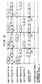
- the transfer information is stored for each item of information in the two shift registers 1A and 1B and thereafter output therefrom. More specifically, unless an interruption signal (d) is sent from the interruption signal generating circuit 13, as shown in Fig. 2, the two items of created information (A) and (B) are stored in the shift registers 1A and 1B, respectively. Thereafter, the transfer information (A) stored in the shift register 1A is serially output and also the transfer information (B) stored in the shift register 1B is serially transferred to the shift register 1A.
- the transfer information once stored in the shift registers 1A and 1B, is automatically output from the signal processing circuit 1 so that output of the transfer information cannot be stopped.
- the interruption generating circuit 13 serves to stop, in terms of an interruption signal (d), storage of the transfer information in the shift registers 1A and 1B in the signal processing circuit to set the wait state for the transfer information.
- the interruption releasing circuit 22 serves to release, by an interruption releasing signal (e), the wait state for the transfer information to permit storage of the transfer information in the shift registers 1A and 1B.
- the signal processing circuit 1 causes two items of transfer information(A) and (B) to be stored in the shift registers 1A and 1B, respectively, and outputs the information serially from the transfer information (A).
- the switch 14 selects the shift register 15 and the selecting circuit 18 selects the shift clock (c) from the frequency dividing circuit 3.
- the transfer information (A) will be passed through the interruption generating circuit 13 and the switch 14 and supplied to the shift register 15; thus the transfer information (A) will be stored in the shift register 15.
- the interruption generating circuit 13 detects the start bit of the transfer information(A) to generate the interruption signal (d) so that the signal processing circuit 1 is placed in a wait condition of inhibiting storage of the subsequent items of information (C) and (D) in the shift registers 1A and 1B.
- the switch 14 When storage of the transfer information (A) in the shift register 15 is completed, the switch 14 is exchanged to the side of the shift register 16 and the selecting circuit 19 selects the shift clock (c) so that the transfer information (B) subsequently output from the signal processing will be stored in the shift register 16. Then, although the interruption generating circuit 13 detects the start bit of the transfer information (B), the signal processing circuit 1 has already been placed in the wait state so that it is not necessarily required to generate the interruption signal (d).
- the selecting circuit 18 selects the shift clock (b) sent from the sync separating circuit 5 so that the transfer information (A) will be serially output from the shift register 15. Then, the switch 21 selects the shift register 15.
- the baud rate of the transfer information (A) output from the shift register 15 is 9600 (bps) which is defined by the shift clock (b), and hence the clock frequency of the reader/writer.
- the transfer information (A) is passed through the switch 21 and the interruption releasing circuit 22 and subjected to the processing for transmission by the transmission circuit 23. Thereafter, the transfer information (A) will be transferred to the reader/writer through the transfer path.
- the interruption releasing circuit 22 detects the stop bit STP of the transfer information (A) to generate an interruption releasing signal, thus releasing the wait state of the signal processing circuit 1.
- the selecting circuit 19 When storage of the transfer information (B) is completed in the shift register 16, the selecting circuit 19 does not select both shift clocks (b) and (c), but places the shift register 16 in a wait condition until read of the transfer information (A) from the shift register 15 is completed.
- the frequency of the shift clock (b) is 9600 Hz
- the transfer information consists of 11 bits
- the switch 21 selects the shift register 16 and the selecting circuit 19 selects the shift clock (b).
- the transfer information (B) is read out serially from the shift register 16, and is supplied to the transmission circuit 23 through the switch 21 and the interruption releasing circuit 22.
- the transfer information (B) is subjected to the processing for transmission by the transmission circuit 23. Thereafter, the transfer information (A) will be transferred to the reader/write through the transfer path.
- the interruption releasing circuit 22 does not generate the interruption releasing signal (e) even if it detects the stop bit of the transfer information (B).
- the interruption releasing circuit 22 when the interruption releasing circuit 22 generates the interruption releasing signal (e) in response to the stop bit STP of the transfer information (A) so that the wait state of the signal processing circuit 1 is released, the subsequent two items of transfer information (C) and (D) stored in the shift registers 1A and 1B will be output in this order.
- the transfer information (C) starts to be output from the signal processing circuit 1 at substantially the same timing as that of starting to read the transfer information (B) from the shift register 16.
- the switch 14 selects the shift register 17 and the selecting circuit 20 selects the shift clock (c).
- the transfer information (C) is stored in the shift register 17.
- the interruption generating circuit 13 detects the start bit ST to generate the interruption signal (d), thus placing the signal processing circuit in a wait state.
- the switch 21 selects the shift register 17 and the selecting circuit 20 selects the shift clock (b) so that the transfer information (C) is read out from the shift register 17 and transferred to the reader/writer.
- the switch 14 selects the shift register 15 and the selecting circuit 18 selects the shift clock (c) so that the subsequent transfer information (D) output from the signal processing circuit 1 is stored in the shift register 15.
- the interruption releasing circuit 22 detects the stop bit STP of the transfer information (C) output from the shift register 17 to generate the interruption releasing signal (e), thereby releasing the wait state of the signal processing circuit 1.
- the interruption releasing circuit 22 detects the stop bit STP of the transfer information (C) output from the shift register 17 to generate the interruption releasing signal (e), thereby releasing the wait state of the signal processing circuit 1.
- write of the subsequent items of transfer information(E) and (F) in the shift registers 1A and 1B is permitted.
- the write of the transfer information (D) in the shift register 15 has been already completed.
- the interruption generating circuit 13 may generate the interruption signal (d) for each start bit of the transfer information supplied.
- the shift registers 15 to 17 can convert the baud rates of data transfer between the reader/writer and the non-contact IC card and also within the non-contact IC card so that they are required rates.
- the signal processing circuit 1 includes two shift registers and the transfer information is output for every two items of information
- shift registers to the number of m (m : integer ⁇ 2) may be provided and the transfer information may be output for every m items of information.
- shift registers to the number of (m + 1) are provided instead of three shift registers 15 to 17, and the interruption releasing circuit 22 generates the interruption releasing signal (e) in response to the stop bit of the (m - 1)-th information of m items of transfer information.
- the receiving coil 6 and the transmission coil 24 are individually provided, one coil having both functions may be used so that the signal passing through a communication control circuit is separately controlled for the receiving circuit 4 and the transmission circuit 23.
- Fig. 4 a modified embodiment is shown.
- reception and transmission of transfer information through input/output coil 6 is carried out by input gate 42, 42', and output gate 41, 41' which are controlled by CPU.
- the oscillator which is inferior to a quartz oscillator in their stability and serves to generate the clock at the frequency different from that of the clock used in the reader/writer can be used as clock generating means to perform the data processing in the signal processing circuit incorporated in a non-contact IC card and the data transfer between it and the reader/writer.
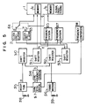
- FIG. 5 is a block diagram of another embodiment of the non-contact IC card according to the present invention.
- 1a and 1b denote memory comprising registers and, for instance, EEPROM.
- the receiving coil 58 is magnetically coupled with the corresponding coil of the reader/writer to form a transfer path
- the transmission coil 59 is also magnetically coupled with the corresponding coil of the reader/writer to form another transfer path.
- the data communication is usually executed in a start-stop synchronization system.
- the data format in the data communication in the start-stop synchronous system is completed of 11 bits consisting of 1 start bit, 8 data bits, 1 parity bit and 1 stop bit. This information composed of 11 bit will be referred to as transfer data.
- the data are usually transferred at the transfer rate (baud rate) of 9600 (bps).
- the transfer data will be transferred with an amplitude-modulated carrier wave, for example.
- the modulated transfer data sent through the coil 58 is received by the receiving circuit 55 and is subjected to the processing such as demodulation.
- the sync signal separating circuit 57 and the frequency dividing circuit 54 separate the sync signal from the received transfer data to produce a shift clock (b) in phase with each of the bits of the transfer data.
- This in-phase signal can be detected in terms of e.g. the edge of the start bit of the demodulated transfer data.
- the shift clock (b) will be produced on the basis of this edge detection timing at the period defined by the above transfer rate of 9600 (bps).
- the transfer data are stored in synchronism with the clock (b) in the shift register 510. As soon as the stop bit of the transfer data (a) has been stored in the shift registers 510, the transfer data (a) of 11 bits are collectively transferred to the shift register 511 and stored therein.
- the clock generated by the clock generating circuit 2 or 53 is supplied to the signal processing circuit 1 which is a CPU (central processing unit) via the clock exchange circuit 4, and the output from the clock generating circuit 2 is supplied to the frequency dividing circuit 515 which frequency-divides the supplied clock to form a shift clock (f).
- the signal processing circuit is driven by a clock to execute the processing such as data processing.
- the transfer data thus received stored in the memory such as an EEPROM by CPU.
- the clock generating circuit 2 is constituted by e.g. a CR oscillator, and generates a clock (d) at the frequency which is always higher than that of the clock (c) output from the sync signal separating circuit 57.
- the clock generating circuit 53 is constituted by e.g. a CR oscillator, and generates a clock (e) at the frequency which is always lower than that of the clock (c) output from the sync signal separating circuit 57. Therefore, the frequency relationship among the clocks (d), (e) and (c) produced from the clock generating circuits 2 and 53, and the sync signal separating circuit 57 can be represented by d > c > e.
- the transfer data of 11 bits are collectively transferred to the shift register 511 and stored therein.
- Each of the bits of the transfer data stored in the shift register 511 is shifted in synchronism with the shift clock (f) to be output one bit by one bit.
- the transfer data will be read out. Since the transfer data are in synchronism with the shift clock (f) which is obtained by frequency-dividing the clock to be supplied to the signal processing circuit 1, the signal processing circuit 1 can process the transfer data. Further, since the shift clock (f) is a relation of f > b with the shift clock (b), the transfer data will never overflow in the shift register.
- the baud rate of the transfer data output from the shift register 511 is always defined by the frequency of the clock generated from the clock generating circuit 2. Therefore, even if the clock frequency in the reader/writer which defines the baud rate of the transfer data received by the receiving circuit 55 is not in a fixed relation with the clock frequency of the clock generating circuit 2 so that the frequencies of the shift clocks (b) and (f) are not equal to each, or the clock frequency of the clock generating circuit 2 is varied, the signal processing circuit 1 can always take in the received transfer data to be processed.
- the clock generating circuit 2 may be a CR oscillator which is inferior to a quartz oscillator in their stability, but can be made small-sized and thin.
- the description hitherto made relates to the operation of data reception in this embodiment. Next, the operation of data transmission will be explained.
- a carrier wave is sent through the receiving coil 58 from the reader/writer. Then, the shift clock at 9600 Hz is produced through the sync signal separating circuit 57 and the frequency dividing circuit 514.
- output transfer data (g) is transferred in synchronism with a shift clock (h) which is obtained by frequency-dividing the clock (e) from the clock generating circuit 53.
- the transfer data are previously stored in the memory such as an EEPROM and their transfer is controlled by CPU.
- the transfer data are stored in the shift register 513 one bit by one bit.
- the transfer data (g) stored in the shift register 512 is transferred to the transmission circuit 56 in synchronism with the shift clock (b) one bit by one bit and thereafter transferred to the reader/writer through the transmission coil.
- the shift registers 510 to 513 can convert the baud rates of data transfer between the reader/writer and the non-contact IC card and also within the non-contact IC card so that they are required rates.
- the receiving coil 58 and the transmission coil 59 are individually provided, one coil having both functions may be used so that the signal passing through a communication control circuit is separately controlled for the receiving circuit 55 and the transmission circuit 56.
- processing speed is increased to realize more rapid processing comparing to conventional IC recording medium in which CPU is operated in synchronism with the synchronization signal supplied from reader/writer since the CPU of this invention is operated by a clock signal of higher frequency than a synchronization signal supplied from the reader/writer.
Landscapes
- Engineering & Computer Science (AREA)
- Physics & Mathematics (AREA)
- Health & Medical Sciences (AREA)
- Computer Networks & Wireless Communication (AREA)
- Toxicology (AREA)
- General Physics & Mathematics (AREA)
- Theoretical Computer Science (AREA)
- Microelectronics & Electronic Packaging (AREA)
- Computer Hardware Design (AREA)
- Electromagnetism (AREA)
- General Health & Medical Sciences (AREA)
- Artificial Intelligence (AREA)
- Computer Vision & Pattern Recognition (AREA)
- Credit Cards Or The Like (AREA)
- Near-Field Transmission Systems (AREA)
Claims (9)
- Kontaktloses IC-Aufzeichnungsmedium (40), mit einer Empfangsspule (6) und einer Sendespule (24) sowie einer Signalverarbeitungsschaltung (1), die beim Senden von Daten als Übertragungsinformationen Daten ausgibt, die für jeweils m Elemente, wobei m eine ganze Zahl ≥ 2 ist, wenigstens mit einem Startbit und mit einem Stoppbit versehen sind, wobei beim Senden und Empfangen von Daten von einer Lese/Schreib-Einrichtung (39) über die Empfangsspule ein Synchronisationssignal (Sync-Signal) empfangen wird, wobei das IC-Aufzeichnungsmedium (40) enthält:eine erste Einrichtung (5) zum Erfassen des Sync-Signals, das von der Lese/Schreib-Einrichtung gesendet wird, um mit der Frequenz, die der Datenübertragungsrate zwischen dem Medium (40) und der Lese/Schreib-Einrichtung (39) entspricht, einen ersten Takt (b) zu erzeugen;eine zweite Einrichtung (2, 3) zum Erzeugen eines zweiten Takts (c), der zum ersten Takt (b) in einer vorgegebenen Frequenzbeziehung steht und eine höhere Frequenz als der erste Takt (b) besitzt, um die Signalverarbeitungsschaltung (1) anzusteuern;eine dritte Einrichtung (15-20) zum Schreiben von Elementen von Übertragungsinformationen, die von der Signalverarbeitungsschaltung ausgegeben werden, unter Verwendung des zweiten Takts (c) in das IC-Aufzeichnungsmedium (40) und zum Lesen der Elemente von Übertragungsinformationen unter Verwendung des ersten Takts (b) sowie zum Übertragen der Elemente von Übertragungsinformationen synchron mit dem ersten Takt (b);eine vierte Einrichtung (13) zum Erzeugen eines Unterbrechungssignals ab dem Startbit wenigstens in dem ersten Element der Übertragungsinformationen der m Elemente der Übertragungsinformationen, die von der Signalverarbeitungsschaltung (1) ausgegeben werden, um die Signalverarbeitungsschaltung (1) in einen Wartezustand zu versetzen, der die nachfolgenden m Elemente von Übertragungsinformationen hält; undeine fünfte Einrichtung (22) zum Erzeugen eines Unterbrechungsbeendigungssignals bei jedem Stoppbit im (m - 1)-ten Element der Übertragungsinformationen, wobei die m Elemente von Übertragungsinformationen von der dritten Einrichtung (15-20) ausgegeben werden, wodurch der Wartezustand der Signalverarbeitungsschaltung (1), der von der vierten Einrichtung (13) gesetzt wird, beendet wird, um die Ausgabe der nachfolgenden m Elemente von Übertragungsinformationen von der Signalverarbeitungsschaltung (1) zuzulassen,wobei die von der dritten Einrichtung (15-20) ausgegebenen Übertragungsinformationen über die Sendespule (24) an die Lese/Schreib-Einrichtung (39) übertragen werden.
- Kontaktloses IC-Aufzeichnungsmedium nach Anspruch 1, bei dem die zweite Einrichtung (2, 3) zum Erzeugen des zweiten Takts (c) ein CR-Oszillator ist.
- Kontaktloses IC-Aufzeichnungsmedium nach Anspruch 2, bei dem die dritte Einrichtung (15-20) Schieberegister (15-17) enthält.
- Kontaktloses IC-Aufzeichnungsmedium nach Anspruch 1, bei dem die Signalverarbeitungsschaltung (1) mehrere Register (1A, 1B) enthält.
- Kontaktloses IC-Aufzeichnungsmedium nach Anspruch 1, wobei das Medium (40) in Form einer Karte entworfen ist.
- Kontaktloses IC-Aufzeichnungsmedium, mit einer Empfangsspule (58), einer Sendespule (59) und einer Signalverarbeitungsschaltung (1), die dazu dienen, das Senden und Empfangen von Signalen in einer Start/Stopp-Synchronisation auszuführen, wobei beim Senden und Empfangen von Daten über die Empfangsspule (58) ein Sync-Signal empfangen wird, mit:einer ersten Einrichtung (57) zum Erfassen des Sync-Signals, das von einer Lese/Schreib-Einrichtung (39) gesendet wird, um mit einer Frequenz, die der Datenübertragungsrate zwischen dem Medium (40) und der Lese/Schreib-Einrichtung (39) entspricht, einen ersten Takt (c) zu erzeugen;einer zweiten Einrichtung (2, 53) zum Erzeugen eines zweiten und eines dritten Takts (d, e), die zum ersten Takt (c) in einer vorgegebenen Frequenzbeziehung stehen, um die Signalverarbeitungsschaltung (1) anzusteuern, wobei die Frequenz des zweiten Takts (d) höher als diejenige des ersten Takts (c) ist und die Frequenz des dritten Takts (e) niedriger als diejenige des ersten Takts (c) ist;einer dritten Einrichtung (512, 513, 514, 517) zum Schreiben von der Signalübertragungsschaltung (1) seriell ausgegebenen Übertragungsdaten unter Verwendung des dritten Takts (e) in das IC-Aufzeichnungsmedium, zum Auslesen der Übertragungsdaten aus dem Medium unter Verwendung des ersten Takts (c) sowie zum Übertragen der Übertragungsdaten unter Verwendung des ersten Takts (c); undeiner vierten Einrichtung (510, 511, 514, 515) zum Schreiben der von der Lese/Schreib-Einrichtung (39) gesendeten Übertragungsdaten unter Verwendung des ersten Takts (c) in das IC-Aufzeichnungsmedium und zum Auslesen der Übertragungsdaten aus dem Medium unter Verwendung des zweiten Takts (d) sowie zum Übertragen der Übertragungsdaten unter Verwendung des zweiten Takts (d) an die Signalverarbeitungsschaltung (1),wobei die von der dritten Einrichtung (512, 513, 514, 517) ausgegebenen Übertragungsdaten an die Lese/Schreib-Einrichtung (39) über die Sendespule (59) übertragen werden.
- Kontaktloses IC-Aufzeichnungsmedium nach Anspruch 6, bei dem eine Frequenzdifferenz oder eine Phasendifferenz zwischen dem ersten Takt (c) und dem zweiten oder dem dritten Takt (d, e) vor dem Beginn des Sendens/Empfangens von Signalen in der Signalverarbeitungsschaltung (1) gespeichert wird und bei dem eine Änderung der Frequenzdifferenz oder der Phasendifferenz erfaßt wird, um die Temperaturänderung im Medium (40) zu erfassen.
- Kontaktloses IC-Aufzeichnungsmedium, mit:einer ersten Einrichtung (5; 57) zum Erfassen eines SYNC-Signals, das von einer Lese/Schreib-Einrichtung (39) gesendet wird, um mit einer Frequenz, die der Datenübertragungsrate zwischen dem Medium (40) und der Lese/Schreib-Einrichtung (39) entspricht, einen ersten Takt (b; c) zu erzeugen;einer zweiten Einrichtung (2, 3; 53) zum Erzeugen eines zweiten Takts (c; d, e), der zum ersten Takt (b; c) in einer vorgegebenen Frequenzbeziehung steht und eine höhere Frequenz als der erste Takt(b; c) besitzt, um eine Signalverarbeitungsschaltung (1) anzusteuern;einer dritten Einrichtung (8, 9, 11, 12; 510, 511) zum Schreiben von Übertragungsinformationen synchron mit einem von der Lese/Schreib-Einrichtung empfangenen Synchronisationssignal in das IC-Aufzeichnungsmedium und zum Auslesen der Übertragungsinformationen aus dem Medium unter Verwendung des zweiten Takts (c, d, e) sowie zum Übertragen der Übertragungsinformationen an die Signalverarbeitungsschaltung (1),wobei eine Verarbeitung der Übertragungsinformationen synchron mit dem zweiten Takt (c; d, e) erfolgt.
- Kontaktloses IC-Aufzeichnungsmedium nach Anspruch 8, bei dem die dritte Einrichtung (8, 9, 11, 12; 510, 511) Schieberegister (8, 9, 510, 511) enthält.
Applications Claiming Priority (2)
| Application Number | Priority Date | Filing Date | Title |
|---|---|---|---|
| JP145507/90 | 1990-06-05 | ||
| JP14550790 | 1990-06-05 |
Publications (3)
| Publication Number | Publication Date |
|---|---|
| EP0460885A2 EP0460885A2 (de) | 1991-12-11 |
| EP0460885A3 EP0460885A3 (en) | 1993-03-31 |
| EP0460885B1 true EP0460885B1 (de) | 1997-04-16 |
Family
ID=15386852
Family Applications (1)
| Application Number | Title | Priority Date | Filing Date |
|---|---|---|---|
| EP91304982A Expired - Lifetime EP0460885B1 (de) | 1990-06-05 | 1991-06-03 | Berührungsloser IC-Aufzeichnungsträger |
Country Status (3)
| Country | Link |
|---|---|
| US (1) | US5353434A (de) |
| EP (1) | EP0460885B1 (de) |
| DE (1) | DE69125652T2 (de) |
Families Citing this family (13)
| Publication number | Priority date | Publication date | Assignee | Title |
|---|---|---|---|---|
| JP3600266B2 (ja) * | 1994-04-08 | 2004-12-15 | 株式会社ルネサステクノロジ | 非接触icカードインタフェース装置及びそれを用いた通信システム |
| JPH07296125A (ja) * | 1994-04-28 | 1995-11-10 | Mitsubishi Denki Semiconductor Software Kk | リーダライタ及び非接触icカードシステム |
| FR2723238B1 (fr) * | 1994-07-27 | 1996-09-13 | Suisse Electronique Microtech | Systeme de communication entre une station de base et un transpondeur passif |
| US5602859A (en) * | 1994-12-19 | 1997-02-11 | Nec Corporation | Start-stop synchronous communicating method capable of correcting improper synchronization and system using the same |
| US6049887A (en) * | 1997-12-04 | 2000-04-11 | Intel Corporation | Method and apparatus for propagating a signal between synchronous clock domains operating at a non-integer frequency ratio |
| JP3666237B2 (ja) * | 1998-03-31 | 2005-06-29 | セイコーエプソン株式会社 | 情報処理装置及び電子機器 |
| JP2001007745A (ja) * | 1999-06-24 | 2001-01-12 | Techno Collage:Kk | 非接触データ転送システム |
| KR100619213B1 (ko) * | 1999-06-29 | 2006-09-01 | 가부시키가이샤 히타치세이사쿠쇼 | 듀얼 인터페이스 ic 카드 |
| EP1102206A1 (de) * | 1999-11-15 | 2001-05-23 | Infineon Technologies AG | Kontaktloser Transponder |
| GB2354603B (en) * | 2000-09-13 | 2002-07-17 | Merrychef Ltd | Programmable cooking systems |
| JP3851766B2 (ja) * | 2000-09-29 | 2006-11-29 | 株式会社ルネサステクノロジ | 半導体集積回路 |
| DE10151889A1 (de) * | 2001-10-24 | 2003-05-08 | Convenience Food Sys Wallau | Verpackungsmaschine |
| JP4036813B2 (ja) * | 2003-09-30 | 2008-01-23 | シャープ株式会社 | 非接触電力供給システム |
Family Cites Families (6)
| Publication number | Priority date | Publication date | Assignee | Title |
|---|---|---|---|---|
| JPS59212949A (ja) * | 1983-05-18 | 1984-12-01 | Dainippon Printing Co Ltd | Icカ−ドの処理方法および処理装置ならびにicカ−ド |
| JPS61226888A (ja) * | 1985-03-30 | 1986-10-08 | Anritsu Corp | Icカ−ド |
| IL82025A (en) * | 1987-03-27 | 1993-07-08 | Galil Electro Ltd | Electronic data communications system |
| EP0309201B1 (de) * | 1987-09-22 | 1993-05-26 | Hitachi Maxell Ltd. | Übertragungsverfahren und -System für kontaktlose I.S.-Karten |
| JPH01118789A (ja) * | 1987-10-30 | 1989-05-11 | Aisan Ind Co Ltd | 情報信号伝送装置 |
| US5099227A (en) * | 1989-07-18 | 1992-03-24 | Indala Corporation | Proximity detecting apparatus |
-
1991
- 1991-06-03 EP EP91304982A patent/EP0460885B1/de not_active Expired - Lifetime
- 1991-06-03 DE DE69125652T patent/DE69125652T2/de not_active Expired - Fee Related
- 1991-06-04 US US07/710,155 patent/US5353434A/en not_active Expired - Lifetime
Also Published As
| Publication number | Publication date |
|---|---|
| US5353434A (en) | 1994-10-04 |
| EP0460885A3 (en) | 1993-03-31 |
| EP0460885A2 (de) | 1991-12-11 |
| DE69125652T2 (de) | 1997-09-11 |
| DE69125652D1 (de) | 1997-05-22 |
Similar Documents
| Publication | Publication Date | Title |
|---|---|---|
| US5353434A (en) | Non-contact IC recording medium | |
| CA1152158A (en) | Battery operated access control card | |
| EP0043432B1 (de) | Schaltungsanordnung zur Fehlererkennung für ein synchrones Datenübertragungssystem | |
| EP0217654A2 (de) | Informationsmedium | |
| EP0282992B1 (de) | Verfahren zur Steuerung der Kommunikation in einem Identifikationssystem | |
| CN105005751B (zh) | 一种rfid标签芯片信号反射方法 | |
| JP2008009910A (ja) | Icカードおよびicカード読み取りシステム | |
| JPH0520513A (ja) | Ic記録媒体 | |
| US4547738A (en) | Phase shift demodulator | |
| US3129409A (en) | Magnetic tape to perforated tape digital information converter | |
| JP2003333112A (ja) | 復調装置 | |
| JPH10173570A (ja) | 非接触icカード装置 | |
| JP2606183B2 (ja) | 情報記憶媒体およびその発行機 | |
| JP3071912B2 (ja) | 半導体記憶媒体へのデータ転送システムにおけるリセット方法およびこの方法の実施に適した半導体記憶媒体 | |
| JP4517281B2 (ja) | 通信装置およびデータ処理方法 | |
| JPH09326015A (ja) | 無接点型メモリカード・システムの通信回路 | |
| JPH10190639A (ja) | クロック乗せ替え回路 | |
| JPH1040346A (ja) | 非接触icカードおよび非接触icカードシステム | |
| JP2912210B2 (ja) | 非同期式シリアルデータ伝送装置 | |
| JP4736197B2 (ja) | リーダライタ | |
| JPH05135220A (ja) | 半導体記憶媒体におけるデータの非接触転送方法 | |
| KR20030002149A (ko) | 콤비카드 | |
| JPH04313146A (ja) | 自動貸し出しシステム | |
| JPH08331189A (ja) | クロック位相同期回路 | |
| JPH1117592A (ja) | 通信装置及び通信システム |
Legal Events
| Date | Code | Title | Description |
|---|---|---|---|
| PUAI | Public reference made under article 153(3) epc to a published international application that has entered the european phase |
Free format text: ORIGINAL CODE: 0009012 |
|
| AK | Designated contracting states |
Kind code of ref document: A2 Designated state(s): DE FR GB |
|
| PUAL | Search report despatched |
Free format text: ORIGINAL CODE: 0009013 |
|
| AK | Designated contracting states |
Kind code of ref document: A3 Designated state(s): DE FR GB |
|
| RHK1 | Main classification (correction) |
Ipc: G06K 7/08 |
|
| 17P | Request for examination filed |
Effective date: 19930716 |
|
| 17Q | First examination report despatched |
Effective date: 19960130 |
|
| GRAG | Despatch of communication of intention to grant |
Free format text: ORIGINAL CODE: EPIDOS AGRA |
|
| GRAH | Despatch of communication of intention to grant a patent |
Free format text: ORIGINAL CODE: EPIDOS IGRA |
|
| GRAH | Despatch of communication of intention to grant a patent |
Free format text: ORIGINAL CODE: EPIDOS IGRA |
|
| GRAA | (expected) grant |
Free format text: ORIGINAL CODE: 0009210 |
|
| AK | Designated contracting states |
Kind code of ref document: B1 Designated state(s): DE FR GB |
|
| REF | Corresponds to: |
Ref document number: 69125652 Country of ref document: DE Date of ref document: 19970522 |
|
| ET | Fr: translation filed | ||
| PLBE | No opposition filed within time limit |
Free format text: ORIGINAL CODE: 0009261 |
|
| STAA | Information on the status of an ep patent application or granted ep patent |
Free format text: STATUS: NO OPPOSITION FILED WITHIN TIME LIMIT |
|
| 26N | No opposition filed | ||
| REG | Reference to a national code |
Ref country code: GB Ref legal event code: IF02 |
|
| PGFP | Annual fee paid to national office [announced via postgrant information from national office to epo] |
Ref country code: FR Payment date: 20050422 Year of fee payment: 15 |
|
| PGFP | Annual fee paid to national office [announced via postgrant information from national office to epo] |
Ref country code: GB Payment date: 20050601 Year of fee payment: 15 |
|
| PGFP | Annual fee paid to national office [announced via postgrant information from national office to epo] |
Ref country code: DE Payment date: 20050829 Year of fee payment: 15 |
|
| PG25 | Lapsed in a contracting state [announced via postgrant information from national office to epo] |
Ref country code: GB Free format text: LAPSE BECAUSE OF NON-PAYMENT OF DUE FEES Effective date: 20060603 |
|
| PG25 | Lapsed in a contracting state [announced via postgrant information from national office to epo] |
Ref country code: DE Free format text: LAPSE BECAUSE OF NON-PAYMENT OF DUE FEES Effective date: 20070103 |
|
| GBPC | Gb: european patent ceased through non-payment of renewal fee |
Effective date: 20060603 |
|
| REG | Reference to a national code |
Ref country code: FR Ref legal event code: ST Effective date: 20070228 |
|
| PG25 | Lapsed in a contracting state [announced via postgrant information from national office to epo] |
Ref country code: FR Free format text: LAPSE BECAUSE OF NON-PAYMENT OF DUE FEES Effective date: 20060630 |