EP0460904A2 - Dispositif de mémoire d'image - Google Patents
Dispositif de mémoire d'image Download PDFInfo
- Publication number
- EP0460904A2 EP0460904A2 EP91305018A EP91305018A EP0460904A2 EP 0460904 A2 EP0460904 A2 EP 0460904A2 EP 91305018 A EP91305018 A EP 91305018A EP 91305018 A EP91305018 A EP 91305018A EP 0460904 A2 EP0460904 A2 EP 0460904A2
- Authority
- EP
- European Patent Office
- Prior art keywords
- memory
- line
- data
- memory array
- serial
- Prior art date
- Legal status (The legal status is an assumption and is not a legal conclusion. Google has not performed a legal analysis and makes no representation as to the accuracy of the status listed.)
- Granted
Links
Images


Classifications
-
- H—ELECTRICITY
- H04—ELECTRIC COMMUNICATION TECHNIQUE
- H04N—PICTORIAL COMMUNICATION, e.g. TELEVISION
- H04N5/00—Details of television systems
- H04N5/76—Television signal recording
- H04N5/907—Television signal recording using static stores, e.g. storage tubes or semiconductor memories
-
- H—ELECTRICITY
- H04—ELECTRIC COMMUNICATION TECHNIQUE
- H04N—PICTORIAL COMMUNICATION, e.g. TELEVISION
- H04N5/00—Details of television systems
- H04N5/04—Synchronising
- H04N5/06—Generation of synchronising signals
- H04N5/067—Arrangements or circuits at the transmitter end
- H04N5/073—Arrangements or circuits at the transmitter end for mutually locking plural sources of synchronising signals, e.g. studios or relay stations
- H04N5/0736—Arrangements or circuits at the transmitter end for mutually locking plural sources of synchronising signals, e.g. studios or relay stations using digital storage buffer techniques
Definitions
- the present invention relates to an image memory device for taking the synchronization of image signals with different timings which signals appear in, for example, a frame synchronizer, a vision mixer, a video switcher or the like.
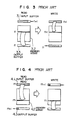
- a line memory 5.3 is provided separately from a field memory 5.2, as shown in Fig. 5, in order to avoid the above-mentioned discontinuity phenomenon.
- the phase of a vertical synchronizing signal on the input side and that of a vertical synchronizing signal on the output side are compared with each other at the bigining of each field.
- a selector 5.4 is switched so that data of a line preceding by 1H than a current line is read and is delivered to a serial output memory, thereby avoiding the passing.
- a signal delayed by 1H is read from the line memory at a synchronized timing so that no discontinuity is produced.
- An object of the present invention is to avoid the discontinuity phenomenon without using such a line memory as mentioned above.
- two free line memories in a memory array of a field memory are used in lieu of an externally mounted line memory and an instruction of bi-directional transfer between an memory array and an output buffer memory is used.
- a separate line memory is not required. Therefore, the number of parts required can be reduced while avoiding the discontinuity phenomenon.
- Fig. 1 is a block diagram of an image memory device according to an embodiment of the present invention.
- reference numeral 1.1 denotes a field memory
- numeral 1.2 a serial input buffer (memory portion) in the field memory 1.1
- numeral 1.3 a memory array portion
- numeral 1.4 an unused or free line A in the memory array
- numeral 1.5 another unused or free line B in the memory array
- numeral 1.6 a serial output buffer memory portion
- numeral 1.7 a memory controller composed of a logic circuit which controls the field memory 1.1.
- bi-directional transfer is possible between the output buffer 1.6 and the memory array 1.3.
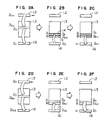
- Figs. 2A to 2F shown the operation of the image memory device for avoiding a motion picture discontinuity phenomenon which is caused by the frame passing phenomenon.
- Figs. 2A, 2B and 2C illustrate the operation of an odd line.
- a difference in phase between a vertical synchronizing signal on the input side and a vertical synchronizing signal on the output side becomes smaller than 0.5H and the (2n-1)th line is to be read/written.
- the (2n-1)th line is written into the memory array 1.3 through the serial input buffer 1.2
- the reading side transfers the 2n-th line of an even line from the memory array 1.3 to the serial output buffer 1.6.
- the 2n-th line data is further transferred to a free line of the memory array 1.3 (a free line A 1.4 in the shown case), as shown in Fig. 2B.
- the (2n-1)th data transferred to another free line (a free line B 1.5 in the shown case) through the above operation before 1H is transferred to the serial output buffer 1.6 as shown in Fig. 2C.
- the (2n-1)th data is simultaneously inputted and outputted. But, since the transfer of data from the memory array 1.3 to the output buffer 1.6 is made in a manner shifted by one line, a discontinuity phenomenon can be avoided even if a frame passing phenomenon occurs.
- the operation of the 2n-th line is shown in Figs. 2D, 2E and 2F.
- the (2n+1)th data is transferred to the serial output buffer 1.6, as shown in Fig. 2D, and is immediately transferred to the free line B 1.5 in the memory array 1.3, as shown in Fig. 2E.
- the 2n-th line data saved before 1H is transferred to the serial output buffer 1.6, as shown in Fig. 2F.
- the above operation is repeated during one field, thereby making it possible to avoid a discontinuity phenomenon.
- an instruction of bi-directional transfer between the serial output buffer 1.6 and the memory array 1.3 is used.
- an instruction of bi-directional transfer between the serial input buffer 1.2 and the memory array 1.3 may be used.
- the data (2n) is written into the memory array 1.3 and data (2n-1) of the memory array 1.3 is read and transferred to the serial output buffer 1.6.
- a motion picture discontinuity phenomenon can be avoided, a frame synchronizer can be constructed at a low cost and with a small size, and the reliability can be improved by the reduction in number of parts. Further, a digital signal pattern on a printed board is reduced. This minimizes undesirable radiation advantageously.
Landscapes
- Engineering & Computer Science (AREA)
- Multimedia (AREA)
- Signal Processing (AREA)
- Studio Circuits (AREA)
- Synchronizing For Television (AREA)
- Television Systems (AREA)
- Image Input (AREA)
- Television Signal Processing For Recording (AREA)
Applications Claiming Priority (2)
| Application Number | Priority Date | Filing Date | Title |
|---|---|---|---|
| JP2147824A JP2699614B2 (ja) | 1990-06-06 | 1990-06-06 | 画像メモリ装置 |
| JP147824/90 | 1990-06-06 |
Publications (3)
| Publication Number | Publication Date |
|---|---|
| EP0460904A2 true EP0460904A2 (fr) | 1991-12-11 |
| EP0460904A3 EP0460904A3 (en) | 1993-01-13 |
| EP0460904B1 EP0460904B1 (fr) | 1997-05-14 |
Family
ID=15439065
Family Applications (1)
| Application Number | Title | Priority Date | Filing Date |
|---|---|---|---|
| EP91305018A Expired - Lifetime EP0460904B1 (fr) | 1990-06-06 | 1991-06-03 | Dispositif de mémoire d'image |
Country Status (4)
| Country | Link |
|---|---|
| US (1) | US5260789A (fr) |
| EP (1) | EP0460904B1 (fr) |
| JP (1) | JP2699614B2 (fr) |
| DE (1) | DE69126061T2 (fr) |
Families Citing this family (1)
| Publication number | Priority date | Publication date | Assignee | Title |
|---|---|---|---|---|
| JP4378015B2 (ja) * | 2000-02-28 | 2009-12-02 | インターナショナル・ビジネス・マシーンズ・コーポレーション | メモリ・チップ |
Family Cites Families (6)
| Publication number | Priority date | Publication date | Assignee | Title |
|---|---|---|---|---|
| JPS59185473A (ja) * | 1983-04-06 | 1984-10-22 | Tokyo Hoso:Kk | テレビジヨン同期変換装置 |
| JPS62206976A (ja) * | 1986-03-06 | 1987-09-11 | Pioneer Electronic Corp | ビデオメモリ−の制御装置 |
| JPS62208766A (ja) * | 1986-03-10 | 1987-09-14 | Mitsubishi Electric Corp | 映像合成装置 |
| JPH07113821B2 (ja) * | 1986-04-21 | 1995-12-06 | 日本テキサス・インスツルメンツ株式会社 | 半導体記憶装置 |
| DE3787324T2 (de) * | 1986-06-20 | 1994-03-31 | Sony Corp | Videospeicher. |
| JPH01224993A (ja) * | 1988-03-04 | 1989-09-07 | Nec Corp | マルチポートメモリ |
-
1990
- 1990-06-06 JP JP2147824A patent/JP2699614B2/ja not_active Expired - Fee Related
-
1991
- 1991-05-28 US US07/705,789 patent/US5260789A/en not_active Expired - Lifetime
- 1991-06-03 EP EP91305018A patent/EP0460904B1/fr not_active Expired - Lifetime
- 1991-06-03 DE DE69126061T patent/DE69126061T2/de not_active Expired - Fee Related
Also Published As
| Publication number | Publication date |
|---|---|
| JP2699614B2 (ja) | 1998-01-19 |
| JPH0440177A (ja) | 1992-02-10 |
| EP0460904A3 (en) | 1993-01-13 |
| DE69126061D1 (de) | 1997-06-19 |
| EP0460904B1 (fr) | 1997-05-14 |
| DE69126061T2 (de) | 1997-11-20 |
| US5260789A (en) | 1993-11-09 |
Similar Documents
| Publication | Publication Date | Title |
|---|---|---|
| EP0502673A2 (fr) | Appareil de commutation de signaux vidéo | |
| US4796089A (en) | Television receiver display apparatus having multi-image display capability | |
| EP0249985A2 (fr) | Mémoire vidéo | |
| EP0122561B1 (fr) | Appareil de synchronisation de signal vidéo de télévision | |
| EP0465007A2 (fr) | Dispositif de commutation de signal vidéo | |
| US6052312A (en) | Multiple-port ring buffer | |
| US4797743A (en) | Video memory control device | |
| US5309233A (en) | Apparatus for converting the scanning period of a video signal to a period not necessarily an integer times the original period | |
| US5260789A (en) | Image memory device | |
| EP0751679B1 (fr) | Appareil d'affichage d'image | |
| EP0462604B1 (fr) | Appareil de correction d'identification de trame | |
| EP0954180B1 (fr) | Appareil pour la transmission en série de données | |
| JPH066764A (ja) | 映像信号処理回路 | |
| JPH06261299A (ja) | スキャンコンバータ | |
| JPH0990920A (ja) | 映像信号変換装置 | |
| JPS58179064A (ja) | フレ−ムメモリ−装置 | |
| JP2799665B2 (ja) | フレーム位相同期装置 | |
| KR100191834B1 (ko) | 휘도신호 및 색신호가 분리 처리되는 텔레비젼 장치 | |
| JP3190711B2 (ja) | 映像走査周波数変換装置の制御方法 | |
| JP2566612B2 (ja) | デュアルポートメモリ用コントロール回路 | |
| JPH0423993B2 (fr) | ||
| JPH05173530A (ja) | 多入力映像信号表示装置 | |
| JP2663484B2 (ja) | メモリ装置 | |
| JPH104526A (ja) | 画像処理装置および処理方法 | |
| JP2001204009A (ja) | 表示装置 |
Legal Events
| Date | Code | Title | Description |
|---|---|---|---|
| PUAI | Public reference made under article 153(3) epc to a published international application that has entered the european phase |
Free format text: ORIGINAL CODE: 0009012 |
|
| AK | Designated contracting states |
Kind code of ref document: A2 Designated state(s): DE FR GB |
|
| PUAL | Search report despatched |
Free format text: ORIGINAL CODE: 0009013 |
|
| AK | Designated contracting states |
Kind code of ref document: A3 Designated state(s): DE FR GB |
|
| 17P | Request for examination filed |
Effective date: 19930225 |
|
| 17Q | First examination report despatched |
Effective date: 19950201 |
|
| GRAG | Despatch of communication of intention to grant |
Free format text: ORIGINAL CODE: EPIDOS AGRA |
|
| GRAH | Despatch of communication of intention to grant a patent |
Free format text: ORIGINAL CODE: EPIDOS IGRA |
|
| GRAH | Despatch of communication of intention to grant a patent |
Free format text: ORIGINAL CODE: EPIDOS IGRA |
|
| GRAA | (expected) grant |
Free format text: ORIGINAL CODE: 0009210 |
|
| AK | Designated contracting states |
Kind code of ref document: B1 Designated state(s): DE FR GB |
|
| REF | Corresponds to: |
Ref document number: 69126061 Country of ref document: DE Date of ref document: 19970619 |
|
| ET | Fr: translation filed | ||
| PLBE | No opposition filed within time limit |
Free format text: ORIGINAL CODE: 0009261 |
|
| STAA | Information on the status of an ep patent application or granted ep patent |
Free format text: STATUS: NO OPPOSITION FILED WITHIN TIME LIMIT |
|
| 26N | No opposition filed | ||
| PGFP | Annual fee paid to national office [announced via postgrant information from national office to epo] |
Ref country code: DE Payment date: 20010528 Year of fee payment: 11 |
|
| PGFP | Annual fee paid to national office [announced via postgrant information from national office to epo] |
Ref country code: GB Payment date: 20010530 Year of fee payment: 11 |
|
| PGFP | Annual fee paid to national office [announced via postgrant information from national office to epo] |
Ref country code: FR Payment date: 20010611 Year of fee payment: 11 |
|
| REG | Reference to a national code |
Ref country code: GB Ref legal event code: IF02 |
|
| PG25 | Lapsed in a contracting state [announced via postgrant information from national office to epo] |
Ref country code: GB Free format text: LAPSE BECAUSE OF NON-PAYMENT OF DUE FEES Effective date: 20020603 |
|
| PG25 | Lapsed in a contracting state [announced via postgrant information from national office to epo] |
Ref country code: DE Free format text: LAPSE BECAUSE OF NON-PAYMENT OF DUE FEES Effective date: 20030101 |
|
| GBPC | Gb: european patent ceased through non-payment of renewal fee |
Effective date: 20020603 |
|
| PG25 | Lapsed in a contracting state [announced via postgrant information from national office to epo] |
Ref country code: FR Free format text: LAPSE BECAUSE OF NON-PAYMENT OF DUE FEES Effective date: 20030228 |
|
| REG | Reference to a national code |
Ref country code: FR Ref legal event code: ST |