EP0460926A2 - Dispositif de reproduction magnétique et dispositif d'enregistrement/de reproduction magnétique - Google Patents
Dispositif de reproduction magnétique et dispositif d'enregistrement/de reproduction magnétique Download PDFInfo
- Publication number
- EP0460926A2 EP0460926A2 EP91305059A EP91305059A EP0460926A2 EP 0460926 A2 EP0460926 A2 EP 0460926A2 EP 91305059 A EP91305059 A EP 91305059A EP 91305059 A EP91305059 A EP 91305059A EP 0460926 A2 EP0460926 A2 EP 0460926A2
- Authority
- EP
- European Patent Office
- Prior art keywords
- carrier
- horizontal synchronizing
- synchronizing pulse
- video signal
- output
- Prior art date
- Legal status (The legal status is an assumption and is not a legal conclusion. Google has not performed a legal analysis and makes no representation as to the accuracy of the status listed.)
- Granted
Links
Images




Classifications
-
- H—ELECTRICITY
- H04—ELECTRIC COMMUNICATION TECHNIQUE
- H04N—PICTORIAL COMMUNICATION, e.g. TELEVISION
- H04N5/00—Details of television systems
- H04N5/76—Television signal recording
- H04N5/91—Television signal processing therefor
- H04N5/92—Transformation of the television signal for recording, e.g. modulation, frequency changing; Inverse transformation for playback
-
- H—ELECTRICITY
- H04—ELECTRIC COMMUNICATION TECHNIQUE
- H04N—PICTORIAL COMMUNICATION, e.g. TELEVISION
- H04N9/00—Details of colour television systems
- H04N9/79—Processing of colour television signals in connection with recording
- H04N9/87—Regeneration of colour television signals
- H04N9/89—Time-base error compensation
Definitions
- the present invention relates to magnetic recording/reproducing apparatus, and more particularly to magnetic recording/reproducing apparatus for recording/reproducing broad-band video signals such as HDTV (High Definition Television) signals.
- HDTV High Definition Television
- a human being is very sensitive in detecting the beat strip which is dynamic distortion, for example, even when the amplitude of a leaking portion of lower sideband of the FM carrier (a peak-peak value) which is a cause of the beat stripe is about 1/200 of the amplitude (a peak-peak value) of a video signal (0.5%, -46dB), the beat stripe is detectable.
- the DU ratio Desired-to-Undesired Signal Ratio
- +35dB is the allowable threshold permittable as to home VTR products.
- J N (m) indicates the Bessel function of the first kind
- ⁇ P indicates the angular frequency of a video signal
- ⁇ C indicates the angular frequency of FM carrier
- ⁇ indicates a value obtained by measuring the phase of the FM carrier (frequency) signal with a reference of a leading edge or a trailing edge of the horizontal synchronizing pulse
- N indicates an integer from - ⁇ to + ⁇ .
- Fig. 7 (a) shows the reference phase of a rise in the leading edge or the trailing edge of a horizontal synchronizing pulse.
- Fig. 7 (b) shows a waveform of a video signal. The video signal is always in synchronization with the horizontal synchronizing pulse.
- the basic wave spectrum of the FM carrier is shown in Fig. 7 (d).
- the first lower sideband and the first upper sideband of the FM carrier are shown in Figs. 7 (e) and (f), respectively.
- Figs. 7 (e) and (f) shows the reference phase of a rise in the leading edge or the trailing edge of a horizontal synchronizing pulse.
- Fig. 7 (b) shows a waveform of a video signal. The video signal is always in synchronization with the horizontal synchronizing pulse.
- the solid line in Fig. 7 (c) indicates a waveform of the
- each phase of the basic wave spectrum, the first lower sideband, and the first upper sideband of the FM carrier is all in synchronization with the reference phase of the leading edge or the trailing edge of the horizontal synchronizing signal. Accordingly, by always maintaining the phase relationship, the phase of the spectrum of the lower sideband which is a cause of the beat stripe occurrence is in synchronization with the horizontal synchronization pulse, resulting in no beat stripes "drifting" on the screen.
- the phase of the spectrum of the first lower sideband and the phase of the spectrum of the first upper sideband also shift by 90° accordingly as shown by the broken lines in Figs. 7 (d), (e) and (f).
- the spectrum of the first lower sideband invades into the band of the demodulated video signal, due to fluctuation in phase ⁇ , the beat stripes appear to drift on the screen.
- the video signal is always in synchronization with the horizontal synchronizing signal as shown in Fig. 7 (b).
- Fig. 3 is a block diagram indicating a schematic structure of an FM modulating/demodulating system of a conventional MUSE ⁇ VTR.
- An inputted MUSE signal to which a negative pole synchronization signal and a reference burst signal are added in a signal processing circuit 31 and the time base compression is applied, is then FM modulated in FM modulator 32 having an AFC (Automatic Frequency Control) circuit to be recorded in magnetic tape 35 through a recording amplifier 33 and a magnetic head.
- AFC Automatic Frequency Control
- Various kinds of timing pulses necessary for operations of signal processing circuit 31 and FM modulator 32 are produced by a timing pulse generator 34 on the basis of the MUSE signal.
- the MUSE signal is time-base compressed to 9/10 times in signal processing circuit 31 for every period of the horizontal synchronizing signal.
- the time-base compressed MUSE signal in which a negative pole synchronizing signal and a reference burst signal are inserted into a blanking time period (about 2.9 ⁇ sec) caused by the time-base compression, is recorded in magnetic tape 35.
- the arrows in Figs. 4 (a), (b) indicate phases at which the positive pole synchronization is conducted.
- the jitter correction of the reproduced signal is executed in a TBC (Time Base Correct) circuit 43 on the basis of the negative pole synchronization signal and the reference burst signal, and then the time-base expansion process of 10/9 times is applied to the reproduced signal in a time base expansion circuit 44 to reproduce an original MUSE signal.
- TBC Time Base Correct
- the band of the MUSE signal provided into signal processing circuit 31 is 8.1MHz, but as a result of the time base compression process of 9/10 times, the required bandwidth becomes 9MHz. Accordingly, as shown in Fig. 5 (a), when the carrier is FM-modulated with a MUSE signal in which a modulation frequency f P of 9MHz is superimposed upon the mid gray level to be recorded in magnetic tape 35, the spectrum of the FM carrier becomes as shown in Fig. 5 (b) in the process of FM demodulation in reproducing. That is to say, in reproducing, the recorded information is picked up by the magnetic head from magnetic tape 35, which is provided as an input to an equalizer 37 through a head amplifier 36. The spectrum of the FM carrier provided as an output from equalizer 37 is shown in Fig. 5 (b).
- the frequency of the center carrier F C is set at 16MHz
- the frequency deviation ⁇ F is set at ⁇ 4MHz
- the input maximum frequency or the modulating frequency F P is set at 9MHz
- the modulation index m1 is set at 0.44.
- the FM carrier outputted from equalizer 37 is provided to a first low-pass filter 38 as shown in Fig. 3.
- the cut-off frequency of the first low-pass filter 38 is defined by the frequency characteristics of an output of the magnetic head, it is defined as 36 MHz for convenience.
- the components of the second lower sideband of the FM carrier (2MHz, the ratio with respect to the carrier, 2.4%) is folded over into the positive frequency range, and if it is demodulated as it is, it comes into the video signal band (9MHz).
- the band of a demodulated video signal (hereinafter, referred to as demodulated video band) is regarded as from -9MHz to +9MHz.
- an output of first low-pass filter 38 is provided to doubler 39 as an input, where the frequency of the FM carrier is doubled.
- the modulation parameters of the FM carrier that is, the frequency of the center carrier F C2 is converted into 32MHz, the frequency deviation ⁇ F2 into ⁇ 8MHz, and the modulation index m2 into 0.89, respectively.
- the second lower side band of the FM carrier is converted into 14MHz, which gets out of the demodulation video band (10MHz). Accordingly, the beat interference is not caused.
- a high-pass filter 40 is provided for cutting off each component of the third lower sideband and the fourth lower sideband of the FM carrier.
- the cut-off frequency of high-pass filter 40 is 10MHz or more.
- An output of high-pass filter 40 is provided to a frequency-doubling FM demodulator of the pulse count type (hereinafter, referred to as a pulse count type FM demodulator) 41 to be demodulated.
- the output of the pulse count type FM demodulator 41 includes besides the demodulated video signal, a doubled FM carrier of the center carrier F C , the frequency deviation ⁇ F, and the modulation index m1, respectively, similarly to the above-mentioned doubler 39. Then, the FM carrier component is provided as an output as it is mixed with demodulated video signal component. Therefore, for eliminating the main FM carrier components and extracting a video signal, a second low-pass filter 42 is provided. That is, as shown in Fig. 3, an output of pulse count type FM demodulator 41 is sent to the second low-pass filter 42. However, a part of the lower sideband of the FM carrier then gets into the demodulation video band, and if the level is higher than an allowable threshold a picture quality deterioration due to the beat interference comes to the fore.
- the FM carrier is quadruple demodulated by the cascade connection of doubler 39 and pulse count type FM demodulator 41
- the modulation parameters of the FM carrier the frequency of the main carrier F C4 into 64MHz, the frequency deviation ⁇ F4 into ⁇ 16MHz, and the modulation index m4 is into about 1.78.
- the demodulation video band is the seventh lower sideband of the FM carrier (1MHz, the ratio with respect to carrier is about 0.01%), and the beat stripes are less than the detectable threshold not to be visible (refer to Fig. 5 (e)).
- the pulse count type FM demodulator 41 for preventing beat stripes is originally unnecessary.
- the first lower sideband (7MHz, the ratio with respect to leak carrier is 21%) of the leak component reaches 4% of the doubled center carrier component, which causes beat stripes.
- a monomultivibrator (not shown) is triggered at the zero cross point of an input carrier, and the output pulses (pulses shown in Fig. 6 (a)-(c)) are averaged by the second low-pass filter 42 to demodulate a video signal.
- the strict condition of satisfying the doubling demodulation in pulse count type FM demodulator 41 is that the inputted FM carrier includes no even number higher harmonic distortion component, especially the second higher harmonic distortion component, and no lower harmonic distortion component, as shown in Fig. 6 (a). That is to say, as shown in that figure (a), when the intervals of zero cross points in the FM carrier are equal (the zero cross point of the basic wave carrier and the zero cross point of the input carrier coincide with each other), there is no leak component from the input carrier, which reduces the lower side band component mixed in the FM demodulation video band.
- the waveform of the input FM carrier is designated by a solid line and the waveform of the basic wave carrier is designated by a broken line.
- the intervals among zero cross points are not equal (zero cross points of the basic wave carrier, zero cross points of the second higher harmonic distortion and zero cross points of the input carrier all differ), and the input leak component is increased/decreased depending on the degree to which extent the intervals between zero cross points differ from an equal interval.
- the center carrier F C2 which is 2 multiplied by doubler 39 includes leak component F C ′ (1/2 lower harmonic distortion component) from the input FM carrier which is not 2 multiplied (refer to Fig. 6 (c))
- the intervals between zero cross points are not equal, so that the leak component is increased/decreased depending on to which extent intervals between zero cross points differ from the equal interval.
- the spectrum of the leak component F C ′ (refer to Fig. 5 (d)) is converted as shown in Fig. 5 (f) by pulse count system FM demodulator 41, and the third lower sideband (5MHz, the ratio with respect to leak carrier is 1.4%) of the leak component F C ′ from the input carrier comes into the FM demodulation video band.
- pulse count system FM demodulator 41 there occur the cross modulation of upper and lower higher harmonic spectrum of the main carrier and the cross modulation of respective higher harmonics of the main carrier and the above leak component.
- the modulation index m1 is large and the spectral spread of the FM carrier spectrum into the upper/lower sidebands is large. Accordingly, when a portion of the lower sidebands of the FM carrier spectrum is cut-off by high-pass filter 40, the upper/lower sidebands are unbalanced, so that inverted white peaks is apt to be caused in an FM demodulation output. Accordingly, it is possible to prevent the inverted white peaks by reducing the spectral spread of the upper/lower sidebands by making the modulation index m1 small to suppress the frequency deviation ⁇ F to around ⁇ 2MHz. However, it has another problem of difficulty in improving the SN ratio of a demodulated video signal.
- providing high-pass filter 40 for preventing beat stripes results in an increase in cost as well as making the structure of an apparatus more complex.
- a magnetic reproducing apparatus reproduces a video signal from a magnetic recording medium in which a carrier FM-modulated with the video signal is recorded.
- the phase of the FM carrier is reset to a reference phase at a leading edge of every horizontal synchronizing pulse during every period of the horizontal synchronizing pulse width in the video signal and fixed to the above reference phase.
- a magnetic reproducing apparatus includes pick-up means for picking up an FM carrier from a magnetic recording medium, and an FM demodulating means for FM-demodulating the FM carrier picked up and converting the same into a video signal.
- the FM demodulating means includes multiplying means for multiplying by 2 M (M is a positive integer) frequency of the picked up FM carrier, and an FM demodulator with a multiplying function for FM-demodulating an output of the multiplying means to convert the same into a video signal having frequency further multiplied by 2 N (N is a positive integer).
- the output of the multiplying means is directly put into the FM demodulator with a multiplying function, and a high-pass filter is not always provided between the multiplying means and the FM demodulator with a multiplying function.
- a magnetic recording/reproducing apparatus in accordance with the present invention includes a recording system for recording a video signal in a magnetic recording medium and a reproducing system for reproducing the video signal from the magnetic recording medium.
- the recording system includes FM modulating means, a reset means and magnetic recording means.
- the FM modulating means provides as an output an FM carrier FM modulated with a video signal.
- the reset means resets the FM modulating means to a reference phase at a leading or trailing edge of every horizontal synchronizing pulse during every period of the horizontal synchronizing pulse width in the video signal, thereby fixes the phase of the FM carrier corresponding to a horizontal synchronizing pulse tip portion (hereinafter called the sync-tip carrier) to the reference phase at every period of the horizontal synchronizing pulse.
- the magnetic recording means magnetically records the FM carrier with phase fixed in the magnetic recording medium.
- the reproducing system has the structure same as that of the above-described magnetic reproducing apparatus according to the present invention.
- the phase of the sync-tip carrier is fixed to a reference phase at the leading edge of horizontal synchronizing pulse, so that if a part of the FM carrier spectrum leaks into the band of the FM demodulation video signal in reproducing, the interference signal due to the leakage appears as reproduced picture distortion in synchronization with a video signal, so that the degree at which a human being detects interference due to the same can be fairly reduced as compared interference due to beat stripes asynchronously drifting with a video signal.
- the frequency deviation quantity of the FM carrier is increased, without cutting off a part of the lower sideband of the FM carrier spectrum with a high-pass filter, the level of the interference can be suppressed to a degree of no practical problem. Accordingly, without causing the inverted white peaks in the FM demodulation video signal, the SN ratio of the FM demodulated video signal can be improved. Also, by omitting a high-pass filter, the structure is simplified and the price can be reduced.
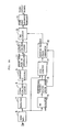
- Fig. 1 is a block diagram showing a structure of an FM modulating system in a recording system of a magnetic recording/reproducing apparatus in accordance with one embodiment of the present invention.
- Fig. 2A is a block diagram indicating a principle structure of an FM demodulating system in a reproducing system of a magnetic recording/reproducing apparatus according to one embodiment of the present invention.
- Fig. 2B is a block diagram indicating more practical structure of an FM demodulating system in a reproducing system of a magnetic recording/reproducing apparatus in accordance with one embodiment of the present invention.
- Fig. 3 is a block diagram indicating a structure of an FM modulating system in a recording system and an FM demodulating system in a reproducing system in a conventional magnetic recording/reproducing apparatus.
- Fig. 4 is a waveform diagram of an input and an output of the signal processing circuit shown in Fig. 3
- Fig. 5 is a waveform diagram of FM carrier spectrum in each portion of the FM demodulating system shown in Fig. 3.
- Fig. 6 is a waveform diagram for describing a frequency-doubling operation in the pulse count type FM demodulator shown in Fig. 3.
- Fig. 7 is a waveform diagram for describing that when a video signal has a horizontal correlation with respect to a horizontal synchronizing pulse and an FM carrier asynchrously drifts with respect to the horizontal synchronizing pulse as shown by the broken line, the asynchrous beat stripes are produced, and that when the phase of the FM carrier or the sync-tip carrier is fixed with respect to the horizontal synchronizing pulse as shown by the solid line, beat stripe component simply distorts the video signal and does not produce the drifting beat stripes or moire.
- Fig. 1 indicates an example of configuring a modulating system
- Fig. 2 indicates an example of configuring a demodulating system.
- Fig. 1 is a block diagram showing one example of an FM modulating system in a recording system of a magnetic recording/reproducing apparatus in accordance with one embodiment of the present invention.
- the FM modulating system mainly includes a signal processing circuit 1, a direct coupling video amplifier 2, an FM modulator 3, a timing signal generator 4, and a frequency discriminator 5 as shown in Fig. 1.
- a record video signal (e.g., a MUSE signal) is provided as an input in signal processing circuit 1.
- An output of signal processing circuit 1 is provided to direct coupling video amplifier 2.
- a frequency discrimination error signal (lower frequency components including a DC component) is fed back from frequency discriminator 5 to signal processing circuit 1.
- the frequency discrimination error signal is summed up upon the record video signal and furthermore, its high frequency component is emphasized.
- an output of signal processing circuit 1 is amplified in direct coupling over a broad-band to be sent to FM modulator 3.
- First and second reset pulses are provided as inputs from timing signal generator 4 to FM modulator 3.
- a clock signal F CK of 9.72MHz which is generated locking to a input a horizontal synchronizing pulse of an input video signal is provided to timing signal generator 4, for example.
- Timing signal generator 4 outputs an AFC reference clock signal, an AFC gate pulse and first and second reset pulses on the basis of these signals F CK and F H .
- the above-mentioned AFC reference clock signal has a frequency (9.72MHz) the same as the clock signal F CK with the frequency equal to the sync-tip carrier frequency.
- the AFC gate pulse is a signal for commanding frequency discriminator 5 to conduct frequency comparison for a period corresponding to the tip portion of the horizontal synchronizing pulse of a recording video signal.
- the first and second reset pulses are for resetting the phase of the sync-tip carrier to the reference phase.
- the pulse for resetting the phase of the sync-tip carrier of FM modulator 3 may be originally a single reset pulse. However, when the reset pulse is single, a rapid change in the phase of FM carrier is caused by resetting to produce large pulse noise at the transient of resetting when FM-demodulating, so that two or more reset pulses are more preferable for moderating the phase change.
- timing signal generator 4 outputs a first reset pulse in the vicinity of the reference phase and resets the phase of the FM carrier corresponding to the above-mentioned tip portion, and outputs the second reset pulse when the reference phase is reached and resets the phase of the sync-tip carrier to a definite phase, which is equivalent to the reference phase with a phase difference of 2 ⁇ N (N is integer).
- N is integer
- FM modulator 3 The output of FM modulator 3 is sent to frequency discriminator 5.
- Frequency discriminator 5 compares the frequency of the AFC reference clock signal and the frequency of the FM carrier provided as an output from FM modulator 3 for the above-mentioned predetermined period.
- the frequency of the FM carrier output and the frequency of the AFC reference clock signal are compared in frequency discriminator 5, and a frequency discrimination error signal corresponding to the frequency difference is fedback to signal processing circuit 1.
- signal processing circuit 1 the frequency discrimination error signal is summed up upon the record video signal and the high band of the video signal is emphasized.
- An output of signal processing circuit 1 after amplified with an appropriate amplification ratio by the DC coupling video amplifier, is superimposed upon the base bias voltage of FM modulator 3. Then, with FM modulator 3, the d.c. component of the base bias voltage increases (or decreases), and the frequency of the FM carrier increases (or decreases) accordingly.
- the FM carrier modulated with the video signal is provided as an output from FM modulator 3.
- the sync-tip carrier is reset to the reference phase with high accuracy, with the result that the transient distortion caused by resetting is reduced.
- a modulating system as disclosed in Japanese Patent Laying-Open No. 63-185177 or 63-274290 may be employed in the present invention.
- An FM carrier reproduced by the magnetic head is supplied to a doubler 9 (square multiplier) in an FM demodulating portion 50 and a gate circuit 17.
- a doubler 9 square multiplier
- an output of doubler 9 is directly inputted to a pulse count type FM demodulator 11. That is to say, in the reproducing system of Fig. 2A, a high-pass filter 40 can be omitted, which was located between doubler 39 and pulse count type FM demodulator 41 for preventing beat stripes in a conventional example (refer to Fig. 3).
- An output of FM demodulating portion 50, or a video signal FM-demodulated is provided as a video signal through TBC (Time Base Correct) circuit 13, and also provided to horizontal synchronizing pulse detector 16.
- Horizontal synchronizing pulse detector 16 separates a horizontal synchronizing pulse from the FM demodulated video signal. The separated horizontal synchronizing pulse is supplied to gate circuit 17 and write-trigger pulse generator 18.
- Gate circuit 17 gates the FM carrier in synchronization with a leading edge of the horizontal synchronizing pulse thereby to extract the sync-tip carrier portion from the FM carrier as a burst signal.
- Write-trigger pulse generator detects a specific zero cross point of the burst signal based on a trailing edge of the horizontal synchronizing pulse and supplies a write-trigger pulse to TBC circuit 13 based on the detected result.
- the FM-demodulated video signal and a portion of the lower sideband of the FM carrier spectrum which invades the demodulation video band are written into a memory of TBC circuit 13.
- the FM carrier can be synchronized with a video signal on a screen and has a horizontal correlation with the demodulated video signal. Accordingly, a portion of the lower sideband of the FM carrier spectrum invading the demodulation video band can be apparently in a still state on the screen.
- the sensitivity of a human being to detect interference of beat stripes asynchronouly drifting on the screen is extremely high, and even if the amplitude of an undesired signal which causes beat stripes is 1/200 times of a video signal amplitude, the beat stripes are detectable. Accordingly, it is said that the permittable limit of the DU ratio in a home video is around 35dB.
- the beat stripes stand still on the screen, the beat stripes appear as reproduced picture distortion, so that the detection sensitivity by a human being is extremely reduced. Accordingly, even if still beat stripes of about 1/20 comes into the reproduced picture, the picture stability may not be degraded.
Landscapes
- Engineering & Computer Science (AREA)
- Multimedia (AREA)
- Signal Processing (AREA)
- Television Signal Processing For Recording (AREA)
Applications Claiming Priority (2)
| Application Number | Priority Date | Filing Date | Title |
|---|---|---|---|
| JP2146503A JPH0824364B2 (ja) | 1990-06-04 | 1990-06-04 | 磁気記録再生装置 |
| JP146503/90 | 1990-06-04 |
Publications (3)
| Publication Number | Publication Date |
|---|---|
| EP0460926A2 true EP0460926A2 (fr) | 1991-12-11 |
| EP0460926A3 EP0460926A3 (en) | 1993-03-03 |
| EP0460926B1 EP0460926B1 (fr) | 1996-12-27 |
Family
ID=15409103
Family Applications (1)
| Application Number | Title | Priority Date | Filing Date |
|---|---|---|---|
| EP91305059A Expired - Lifetime EP0460926B1 (fr) | 1990-06-04 | 1991-06-04 | Dispositif d'enregistrement magnétique et dispositif d'enregistrement/de reproduction magnétique |
Country Status (6)
| Country | Link |
|---|---|
| US (1) | US5260838A (fr) |
| EP (1) | EP0460926B1 (fr) |
| JP (1) | JPH0824364B2 (fr) |
| CA (1) | CA2043772C (fr) |
| DE (1) | DE69123786T2 (fr) |
| ES (1) | ES2095910T3 (fr) |
Cited By (1)
| Publication number | Priority date | Publication date | Assignee | Title |
|---|---|---|---|---|
| EP0512369A3 (en) * | 1991-05-06 | 1993-08-04 | Nokia (Deutschland) Gmbh | Luminance transmission channel for a videorecorder |
Family Cites Families (7)
| Publication number | Priority date | Publication date | Assignee | Title |
|---|---|---|---|---|
| US4591930A (en) * | 1983-09-23 | 1986-05-27 | Eastman Kodak Company | Signal processing for high resolution electronic still camera |
| JPS63102481A (ja) * | 1986-10-18 | 1988-05-07 | Pioneer Electronic Corp | 多重記録方式 |
| US4843334A (en) * | 1986-12-09 | 1989-06-27 | Canon Kabushiki Kaisha | Frequency demodulator operable with low frequency modulation carriers |
| JPS63185177A (ja) * | 1987-01-27 | 1988-07-30 | Sony Corp | 周波数変調回路 |
| JPH0632467B2 (ja) * | 1987-05-01 | 1994-04-27 | シャープ株式会社 | Vtr記録再生映像信号のジッタ検出方法 |
| US5045950A (en) * | 1987-05-01 | 1991-09-03 | Sharp Kabushiki Kaisha | Circuit for detecting and compensating for jitter produced by a recording/reproducing apparatus |
| JP2507821B2 (ja) * | 1990-03-13 | 1996-06-19 | シャープ株式会社 | キャリアリセットfm変調器 |
-
1990
- 1990-06-04 JP JP2146503A patent/JPH0824364B2/ja not_active Expired - Lifetime
-
1991
- 1991-05-31 US US07/708,927 patent/US5260838A/en not_active Expired - Fee Related
- 1991-06-03 CA CA002043772A patent/CA2043772C/fr not_active Expired - Fee Related
- 1991-06-04 EP EP91305059A patent/EP0460926B1/fr not_active Expired - Lifetime
- 1991-06-04 DE DE69123786T patent/DE69123786T2/de not_active Expired - Fee Related
- 1991-06-04 ES ES91305059T patent/ES2095910T3/es not_active Expired - Lifetime
Cited By (1)
| Publication number | Priority date | Publication date | Assignee | Title |
|---|---|---|---|---|
| EP0512369A3 (en) * | 1991-05-06 | 1993-08-04 | Nokia (Deutschland) Gmbh | Luminance transmission channel for a videorecorder |
Also Published As
| Publication number | Publication date |
|---|---|
| US5260838A (en) | 1993-11-09 |
| JPH0824364B2 (ja) | 1996-03-06 |
| JPH0440089A (ja) | 1992-02-10 |
| EP0460926A3 (en) | 1993-03-03 |
| DE69123786D1 (de) | 1997-02-06 |
| DE69123786T2 (de) | 1997-05-28 |
| EP0460926B1 (fr) | 1996-12-27 |
| CA2043772C (fr) | 1995-05-23 |
| CA2043772A1 (fr) | 1991-12-05 |
| ES2095910T3 (es) | 1997-03-01 |
Similar Documents
| Publication | Publication Date | Title |
|---|---|---|
| US5465071A (en) | Information signal processing apparatus | |
| US4110785A (en) | Clock generator for video signal processing | |
| EP0289046B1 (fr) | Dispositif détecteur de fluctuations de base de temps pour un enregistreur à bande vidéo | |
| US5191434A (en) | Synchronizing signal restoration circuit | |
| JPS63185177A (ja) | 周波数変調回路 | |
| JPH0557798B2 (fr) | ||
| EP0460926B1 (fr) | Dispositif d'enregistrement magnétique et dispositif d'enregistrement/de reproduction magnétique | |
| US3715474A (en) | Color video recording and playback system | |
| US3749835A (en) | Continuous signal producing system | |
| KR940008846B1 (ko) | 자기재생장치 및 자기 기록재생장치 | |
| EP0161810B1 (fr) | Appareil de traitement de signaux de chrominance | |
| US4323915A (en) | Method and an apparatus for video tape recording | |
| US3777060A (en) | Color television signal recording and reproducing system | |
| US5598274A (en) | Image signal recording and reproducing system | |
| RU2072565C1 (ru) | Устройство для записи-воспроизведения опорного сигнала корректора временных искажений в видеомагнитофоне | |
| EP0522867B1 (fr) | Dispositif de reproduction magnétique | |
| JPS63274290A (ja) | Vtr記録再生映像信号のジッタ検出方法 | |
| JPS6364488A (ja) | 磁気記録再生方式 | |
| JPS6015195B2 (ja) | 搬送色信号の処理回路 | |
| JPS605117B2 (ja) | カラービデオ信号の記録再生方式 | |
| JPH0625103Y2 (ja) | 外部リセット機能付きfm変調回路 | |
| JPS62265876A (ja) | 映像信号記録再生装置の時間軸補正装置 | |
| JPH03113974A (ja) | 映像信号記録再生装置 | |
| JPH0646455A (ja) | 磁気再生装置 | |
| JPH0722375B2 (ja) | 磁気記録再生装置 |
Legal Events
| Date | Code | Title | Description |
|---|---|---|---|
| PUAI | Public reference made under article 153(3) epc to a published international application that has entered the european phase |
Free format text: ORIGINAL CODE: 0009012 |
|
| AK | Designated contracting states |
Kind code of ref document: A2 Designated state(s): DE ES FR GB NL |
|
| PUAL | Search report despatched |
Free format text: ORIGINAL CODE: 0009013 |
|
| AK | Designated contracting states |
Kind code of ref document: A3 Designated state(s): DE ES FR GB NL |
|
| 17P | Request for examination filed |
Effective date: 19930826 |
|
| 17Q | First examination report despatched |
Effective date: 19950609 |
|
| GRAG | Despatch of communication of intention to grant |
Free format text: ORIGINAL CODE: EPIDOS AGRA |
|
| GRAH | Despatch of communication of intention to grant a patent |
Free format text: ORIGINAL CODE: EPIDOS IGRA |
|
| RTI1 | Title (correction) | ||
| GRAH | Despatch of communication of intention to grant a patent |
Free format text: ORIGINAL CODE: EPIDOS IGRA |
|
| GRAA | (expected) grant |
Free format text: ORIGINAL CODE: 0009210 |
|
| AK | Designated contracting states |
Kind code of ref document: B1 Designated state(s): DE ES FR GB NL |
|
| REF | Corresponds to: |
Ref document number: 69123786 Country of ref document: DE Date of ref document: 19970206 |
|
| ET | Fr: translation filed | ||
| REG | Reference to a national code |
Ref country code: ES Ref legal event code: FG2A Ref document number: 2095910 Country of ref document: ES Kind code of ref document: T3 |
|
| PLBE | No opposition filed within time limit |
Free format text: ORIGINAL CODE: 0009261 |
|
| STAA | Information on the status of an ep patent application or granted ep patent |
Free format text: STATUS: NO OPPOSITION FILED WITHIN TIME LIMIT |
|
| 26N | No opposition filed | ||
| PGFP | Annual fee paid to national office [announced via postgrant information from national office to epo] |
Ref country code: DE Payment date: 20010528 Year of fee payment: 11 |
|
| PGFP | Annual fee paid to national office [announced via postgrant information from national office to epo] |
Ref country code: GB Payment date: 20010530 Year of fee payment: 11 |
|
| PGFP | Annual fee paid to national office [announced via postgrant information from national office to epo] |
Ref country code: FR Payment date: 20010611 Year of fee payment: 11 |
|
| PGFP | Annual fee paid to national office [announced via postgrant information from national office to epo] |
Ref country code: NL Payment date: 20010628 Year of fee payment: 11 |
|
| PGFP | Annual fee paid to national office [announced via postgrant information from national office to epo] |
Ref country code: ES Payment date: 20010629 Year of fee payment: 11 |
|
| REG | Reference to a national code |
Ref country code: GB Ref legal event code: IF02 |
|
| PG25 | Lapsed in a contracting state [announced via postgrant information from national office to epo] |
Ref country code: GB Free format text: LAPSE BECAUSE OF NON-PAYMENT OF DUE FEES Effective date: 20020604 |
|
| PG25 | Lapsed in a contracting state [announced via postgrant information from national office to epo] |
Ref country code: ES Free format text: LAPSE BECAUSE OF NON-PAYMENT OF DUE FEES Effective date: 20020605 |
|
| PG25 | Lapsed in a contracting state [announced via postgrant information from national office to epo] |
Ref country code: NL Free format text: LAPSE BECAUSE OF NON-PAYMENT OF DUE FEES Effective date: 20030101 Ref country code: DE Free format text: LAPSE BECAUSE OF NON-PAYMENT OF DUE FEES Effective date: 20030101 |
|
| GBPC | Gb: european patent ceased through non-payment of renewal fee |
Effective date: 20020604 |
|
| PG25 | Lapsed in a contracting state [announced via postgrant information from national office to epo] |
Ref country code: FR Free format text: LAPSE BECAUSE OF NON-PAYMENT OF DUE FEES Effective date: 20030228 |
|
| NLV4 | Nl: lapsed or anulled due to non-payment of the annual fee |
Effective date: 20030101 |
|
| REG | Reference to a national code |
Ref country code: FR Ref legal event code: ST |
|
| REG | Reference to a national code |
Ref country code: ES Ref legal event code: FD2A Effective date: 20030711 |