EP0461615A2 - Appareil de prise de vues en couleurs - Google Patents
Appareil de prise de vues en couleurs Download PDFInfo
- Publication number
- EP0461615A2 EP0461615A2 EP91109567A EP91109567A EP0461615A2 EP 0461615 A2 EP0461615 A2 EP 0461615A2 EP 91109567 A EP91109567 A EP 91109567A EP 91109567 A EP91109567 A EP 91109567A EP 0461615 A2 EP0461615 A2 EP 0461615A2
- Authority
- EP
- European Patent Office
- Prior art keywords
- signal
- circuit
- above described
- color image
- signal level
- Prior art date
- Legal status (The legal status is an assumption and is not a legal conclusion. Google has not performed a legal analysis and makes no representation as to the accuracy of the status listed.)
- Granted
Links
Images









Classifications
-
- H—ELECTRICITY
- H04—ELECTRIC COMMUNICATION TECHNIQUE
- H04N—PICTORIAL COMMUNICATION, e.g. TELEVISION
- H04N9/00—Details of colour television systems
- H04N9/64—Circuits for processing colour signals
- H04N9/646—Circuits for processing colour signals for image enhancement, e.g. vertical detail restoration, cross-colour elimination, contour correction, chrominance trapping filters
-
- H—ELECTRICITY
- H04—ELECTRIC COMMUNICATION TECHNIQUE
- H04N—PICTORIAL COMMUNICATION, e.g. TELEVISION
- H04N23/00—Cameras or camera modules comprising electronic image sensors; Control thereof
- H04N23/80—Camera processing pipelines; Components thereof
- H04N23/84—Camera processing pipelines; Components thereof for processing colour signals
- H04N23/843—Demosaicing, e.g. interpolating colour pixel values
-
- H—ELECTRICITY
- H04—ELECTRIC COMMUNICATION TECHNIQUE
- H04N—PICTORIAL COMMUNICATION, e.g. TELEVISION
- H04N5/00—Details of television systems
- H04N5/14—Picture signal circuitry for video frequency region
- H04N5/20—Circuitry for controlling amplitude response
- H04N5/205—Circuitry for controlling amplitude response for correcting amplitude versus frequency characteristic
- H04N5/208—Circuitry for controlling amplitude response for correcting amplitude versus frequency characteristic for compensating for attenuation of high frequency components, e.g. crispening, aperture distortion correction
-
- H—ELECTRICITY
- H04—ELECTRIC COMMUNICATION TECHNIQUE
- H04N—PICTORIAL COMMUNICATION, e.g. TELEVISION
- H04N25/00—Circuitry of solid-state image sensors [SSIS]; Control thereof
- H04N25/10—Circuitry of solid-state image sensors [SSIS]; Control thereof for transforming different wavelengths into image signals
- H04N25/11—Arrangement of colour filter arrays [CFA]; Filter mosaics
- H04N25/13—Arrangement of colour filter arrays [CFA]; Filter mosaics characterised by the spectral characteristics of the filter elements
- H04N25/135—Arrangement of colour filter arrays [CFA]; Filter mosaics characterised by the spectral characteristics of the filter elements based on four or more different wavelength filter elements
- H04N25/136—Arrangement of colour filter arrays [CFA]; Filter mosaics characterised by the spectral characteristics of the filter elements based on four or more different wavelength filter elements using complementary colours
Definitions
- the present invention generally relates to a color image pickup apparatus for correcting the sharpness of the luminance signal in a color image pickup system for taking out as different color signals for each of the horizontal lines the color information from the objects to be photographed with the use of a color image sensor having a color filter arrangement face.
- color image pickup apparatuses with the use of a color image sensor are being popularized quickly by the best use of the characteristics of the smaller size and the lighter weight, and by the advancement in the higher performance.
- the various types of automatic correctors are further equipped with as higher tendencies.
- Image pickup apparatuses which are capable of coping with any objects to be photographed are expected.
- the resolution feelings of the finishing screen are improved. Therefore, the automatic adjustment of the sharpness becomes important in the color image pickup apparatuses.
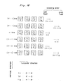
- FIG. 16 An example of the color filters of a color image sensor for taking out the color information from the photographed objects as different color signals for each of the horizontal lines with the mosaic shaped color filters being arranged on the front face is shown in Fig. 16.
- the conventional construction example of the luminance signal processing portion of the color image pickup apparatus is shown in Fig. 21.
- the signal to be obtained from the color image sensor 1 is guided into a luminance signal separating circuit 4 and a vertical sharpness correcting signal generating circuit 3.
- the outputs of both the circuits are added by an adding circuit 6 and the luminance signal with the sharpness of the vertical direction being emphasized therein is obtained.
- the vertical sharpness correcting signal generating circuit 3 is composed of, for example, one horizontal scanning period delaying circuit (hereinafter 1H delaying circuit) 81, a subtracter 82 for getting the difference signal between the 1H delaying circuit output and the signal not to be delayed by 1H, a low-pass filter (hereinafter referred to as LPF) 83 and an amplifier 84.
- 1H delaying circuit one horizontal scanning period delaying circuit
- LPF low-pass filter
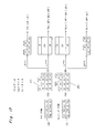
- the signal to be changed for each of such picture elements as shown in Fig. 17 (a), (c) is outputted from the color image sensor 1.
- the signal to be changed for each of such picture elements as shown in Fig. 17 (b), (d) is outputted from the color image sensor 1. From the nH line or the n'H line, the luminance signal of 2R + 3G + 2B is obtained as the low-pass signal, the color difference signal of 2B-G is obtained as the high frequency modulating signal.
- the characteristic graph of Fig. 18 shows the relationship between the output level (signal level) of these signals and the size (input light level) of the input light of the color image sensor 1.
- the straight lines (a) and (b) of Fig. 18 respectively show the signals of the picture elements Ye and Mg of the (n + 1)H line or the (n + 1)'H line and the signals of the picture elements of Cy and G.
- One dot chain line (e) shows the average value of both the picture elements, namely, the low-pass signal (luminance signal).
- the dot lines (c) and (d) of Fig. 18 respectively show the signals of the picture elements of the nH line or n'H line Cy and Mg and the signals of the picture elements of Ye and G.
- one dot chain line (f) shows the average value of both the picture elements, namely, the low-pass signal (luminance signal). Therefore, the processing of the luminance signal separating circuit 4 basically becomes the processing for removing the high-pass modulating signal through the low-pass filter in the output signalof the color image sensor. As shown in the wave form chart in Fig.
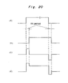
- the processing of the vertical sharpness correcting signal generating circuit 3 becomes the processing for removing the high frequency modulating signal so as to amplify the proper magnification through the LPF 83 in the difference signal (Fig. 20, the wave form (c)) between the output signal (Fig. 20, the wave form (a)) of the color image sensor 1 and the output signal (Fig. 20, the waver form (b)) of the color image sensor 1 delayed by one horizontal scanning period. Accordingly, the luminance signal with such vertical sharpness shown in Fig. 20, the wave form (d) being corrected therein is obtained into the output of the adding circuit 6 of Fig. 21.
- the luminance signal to be obtained from the color image sensor 1 is an average signal of two picture elements adjacent to the respective horizontal lines, the value thereof becoming equal in each horizontal line in principle (unless the object to be photographed changes). For example, as the incident light quantity becomes large, the signal from the picture element for generating the large signal level out of the respective picture elements of the color image sensor begins its saturation, with a problem that the luminance signal level of the adjacent two horizontal lines does not conform to each other before all the signals of the other picture elements are saturated. This situation will be described in detail with the use of Fig. 18, Fig. 19, Fig. 22. In the characteristics graph of the above described Fig.
- the luminance signal level (shown in one dot chain lines (e), (f) in Fig. 18) of the adjacent two horizontal lines agrees with each other from the saturation level S sat of the color image sensor 1 to the incident light quantity L1 where the signal level of each picture element is small.
- the signals of the picture elements of the (n+1)H line or the (n+1)'H line Ye and Mg shown in the straight line (a) of Fig. 18 are saturated at the S sat.
- nH line or n'H line luminance signal does not change in the addition of the signal level accompanied by the incident light quantity increase like a straight line (f) in Fig. 18, while the (n+1)H line or the (n+1)'H line luminance signal becomes smaller in the signal level increase accompanied by the incident light quantity increase like a straight line (e) in Fig. 18, thus causing the difference in the luminance signal level of two horizontal lines.
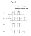
- Fig. 19 shows a signal wave form chart for each picture element of the respective horizontal lines.
- Fig. 19 (a) shows the signal level for each of the (n+1)H line or the (n+1)'H line picture element, with the larger one showing the signal of the picture elements of the Ye and the Mg.
- Fig. 19 (b) shows the signal level of each picture element of the nH line or the n'H line.
- the wave form (a) of Fig. 22 is the output signal from the color image sensor 1, which has the signal level difference of the dS between the adjacent lines.
- the wave form (b) of Fig. 22 is a signal thereof delayed by 1H.
- the wave form (c) of Fig. 22 is a difference signal between the wave form (a) and the wave form (b), and becomes a vertical sharpness correcting signal.
- the signal level difference dS' between two lines of the output luminance signal corrected in the vertical sharpness shown in the wave form (d) of Fig. 22 becomes larger than the level difference dS in the input signal.
- the signal is saturated by the color image sensor 1
- these circuits may be saturated earlier than the color image sensor 1 in, for example, the construction where the amplification circuit and the A/D converting circuit have been arranged immediately after the color image sensor 1 without restriction to this example. Even in these cases, the same problem as described hereinabove occurs.
- the present invention has been developed with a view to substantially eliminating the above discussed drawbacks inherent in the prior art, and has for its essential object to provide an improved color image pickup apparatus.
- Another important object of the present invention is to provide an improved color image pickup apparatus, which does not emphasize it, and is capable of correcting it even when the signals are saturated in the image sensor and the signal level between the adjacent two horizontal lines has been different in spite of the photographing the object which is the same in the signal level between two adjacent horizontal lines.
- Still another important object of the present invention is to provide a color image pickup apparatus which has the correction and the vertical sharpness emphasis.
- a color image pickup apparatus which includes a color solid image pickup element for taking out the color information from the object to be photographed, as a color signal different for each of the horizontal lines having a color filter arrangement, a signal level detecting circuit for detecting the signal level for each of the picture elements of the image sensor, a luminance signal separating circuit for separating the luminance signal from the output signal of the image sensor, a correcting signal generating circuit for generating the correcting signal for correcting the sharpness in the vertical direction from the output signal of the above described luminance signal, a controlling circuit for controlling the signal level of the correcting signal or the polarity and signal level by the signal level detecting output, an adding circuit for composing the output signal of the control circuit and the above described luminance signal.
- the signal level for each of the picture elements of the color image sensor is detected by the signal level detecting circuit.
- the signal level of the vertical sharpness correcting signal is made smaller or the polarity is reversed, so that the difference of the signal level between the adjacent two horizontal lines is not emphasized even when the signals are saturated by the image sensor and so on. Further, the correcting operation may be effected. Then, the correction and the vertical sharpness emphasis are adapted to be provided with.
- a color image pickup apparatus which includes a color image sensor for taking out the color information from the object to be photographed, as a color signal different for each of the horizontal lines having a color filter arrangement, a signal level detecting circuit for detecting the signal level for each of the picture elements of the image sensor, an adding circuit for composing the signal of at least two horizontal lines of the output signal of the image sensor, a switching circuit for switching the output signal of the adding circuit and the output signal of the image sensor by the output signal of the signal level detecting circuit, a luminance signal separating circuit for obtaining the luminance signal from the switching circuit output signal, with the switching circuit being adapted to select the adding circuit output when the signal level detecting circuit output has been caused.
- the signal level for each of the picture elements of the color image sensor is detected by the signal level detecting circuit.
- the luminance signal is obtained from the average signals of the adjacent horizontal lines when the signal level is larger than the reference level. Even when the signal is saturated by the image sensor and so on, and the signal level between the adjacent two horizontal lines, this is adapted to be corrected.
- a third invention is a color image pickup apparatus which includes a color image sensor for taking out as the different color signal for each of horizontal lines the color signal from the object to be photographed having a color filter arrangement, a signal level detecting circuit for detecting the signal level for each of the picture elements of the color image sensor and generating the control signals when the signal level is larger than the reference level, a first delaying circuit for delaying by one horizontal scanning period the output signal of the solid image pickup element, a second delaying circuit for delaying by one horizontal scanning period the output signal of the first delaying circuit, a first adding circuit for adding the output signal of the color image sensor and the output signal of the second delaying circuit, a multiplying circuit for making the output signal of the first adding circuit one time / two times, a second adding circuit for adding the output signal of the first delaying circuit and the output signal of the multiplying circuit, a subtracter for subtracting the output signal of the multiplying circuit from the output signal of the first delaying circuit, a separating circuit for separating the luminance signal from the output signal of the second
- the luminance signal is obtained from the weighted average signal of the adjacent three horizontal lines, the signal level for each of the picture elements of the color image sensor is detected by the signal level detecting circuit.
- the signal level of the vertical sharpness correcting signal is made smaller, so that it is corrected even when the signal is saturated by the image sensor and the signal level between the adjacent two horizontal lines are different, and also, the vertical sharpness emphasis is normally adapted to be effected.
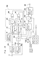
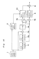
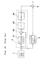
- Fig. 1 is a block diagram showing the basic construction of a first invention of the present invention.
- Reference numeral 1 is a color image sensor with color filters shown in Fig. 16 being arranged on them.
- the signals to be obtained from the color image sensor 1 and the processing of obtaining the luminance signals from the signals will be described in detail hereinafter.
- the signals to be changed for each of the picture elements as shown in Fig. 17 (a), (c) are outputted from the color image sensor 1.
- the luminance signals of 2R + 3G + 2B are obtained as low-pass signals, the color difference signals of 2B - G are obtained as the high frequency modulating signals from the nH line or the n'H line.
- the luminance signals of 2R + 3G + 2B are obtained as the low-pass signals, the color difference signal of 2R - G are obtained as the high frequency modulating signals from the (n+1)H line or the (n+1)'H line.
- the characteristics chart of Fig. 18 shows the relationship between the output level (signal level) of these signals and the size (input light level) of the input light of the color image sensor 1. Namely, the straight lines (a) and (b) of Fig.
- the one dot chain line (e) thereof shows the average value of both the picture elements, namely, the low-pass signal (luminance signal), also, the dot lines (c) and (d) of Fig. 18 show respectively the signals of the picture elements of the nH line or n'H line of Cy and Mg, and the signals of the picture elements of the Ye and the G, also one dot chain line (f) shows the average value of both the picture elements, namely, the low-pass signal (luminance signal).
- the luminance signal separation processing basically removes the high-pass modulating signal through the low-pass filter in the output signal of the color image sensor.
- the vertical sharpness correcting signal generating processing removes the high frequency modulating signal through the low-pass filter (LPF) in the difference signal (Fig. 20, the wave form (c)) between the output signal (Fig. 20, the wave form (a) of the color image sensor 1 and the output signal (Fig. 20, the wave form (b)) of the color image sensor 1 delayed by one horizontal scanning period so as to effect the amplification of the proper multiplying factor.
- the output signal of the color image sensor 1 is guided into the vertical sharpness correcting signal generating circuit 3 and the luminance signal separating circuit 4 and is guided into the signal level detecting circuit 2 so as to detect the signal level for each picture element.
- the output signal of the signal level detecting circuit 2 controls the signal from the vertical sharpness correcting signal generating circuit 3 by the control circuit 5, and the output signal of the control circuit 5 is added to the above described luminance signal separating circuit 4 by the adding circuit 6.
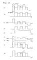
- the first embodiment in the basic construction will be described hereinafter in detail with the use of the wave form chart of Fig. 2.
- the embodiment is an example where the control circuit 5 controls the stopping of the signal from the vertical sharpness correcting signal generating circuit 3.
- the wave form expressing for each horizontal period (hereinafter referred to as 1H period)
- the output signal of the color image sensor becomes a signal having the level difference for each 1H in Fig. 2, the wave form (a).
- the difference signal between the signal and the signal delayed by 1H (Fig. 2, the wave form (b)) becomes Fig. 2, the wave form (c).
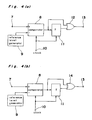
- Fig. 4 (a) The construction shown in, for example, Fig. 4 (a) is considered as the first example of the signal level detecting circuit 2.
- the signal of the color image sensor 1 is guided into the input terminal 7 so as to compare for each picture element with the reference level from the reference level generator 9 by the comparator 8.
- the output of the comparator 8 is guided into the 1 picture element delaying circuit 11, and also, the "or" with respect to the output of the 1 picture element delaying circuit 11 is provided by the "or” circuit 12.
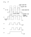
- the signal to be inputted into the input terminal 7 is such a wave form signal as shown in Fig. 5 (a), and the reference level is a value a little smaller than the saturation level of Fig.
- the output of the comparator 8 becomes a signal high at level at the timing of the picture element saturated at the signal level as shown in Fig. 5 (c), and becomes a signal low at level at the timing of the picture element not saturated at the signal level. Therefore, the output of the 1 picture element delaying circuit 11 becomes the wave form (d) of Fig. 5, the output of the "or" circuit 12, namely, the output of the signal level detecting circuit 2 becomes a signal shown in the wave form (e) in Fig. 5.
- the clock which is in conformity with the picture element period is guided into the comparator 8 and 1 picture element delaying circuit 11 and is capable of comparison and 1 clock of delaying for each picture element.
- the wave form (e) is provided as Fig. 2, the wave form (d) when it is expressed for each 1H period.
- the control circuit 5 controls the stopping of the signal from the vertical sharpness correcting signal generating circuit 3. Therefore, the controlled vertical sharpness correcting signal becomes a signal shown in Fig. 2, the wave form (e).
- the output signal to be obtained from the adding circuit 6 is provided in Fig. 2, the wave form (f).
- the signal level difference for each 1H period becomes dS'' and becomes larger than the level difference dS of the original signal, but becomes smaller than the level difference dS' in the conventional example of Fig. 22 (d), thus resulting in effects in the present embodiment.
- Fig. 4 (b) is a second example of a signal level detecting circuit 2).
- the "or" circuit 12 in a first example shown in Fig. 4 (a) is provided as an exclusive or circuit 14, and the saturation detecting signal is adapted not to be outputted when both the two picture elements adjacent in the horizontal direction have been saturated.
- the saturation detecting signal is adapted not to be outputted when both the two picture elements adjacent in the horizontal direction have been saturated.
- the saturation detecting signal is adapted not to be outputted when both the two picture elements adjacent in the horizontal direction have been saturated.
- the saturation detecting signal is adapted not to be outputted when both the two picture elements adjacent in the horizontal direction have been saturated.
- the saturation detecting signal is adapted not to be outputted when both the two picture elements adjacent in the horizontal direction have been saturated.
- the saturation detecting signal is adapted not to be outputted when both the two picture elements adjacent in the horizontal direction have been saturated.
- the saturation detecting signal is adapted not to be outputted when both the two picture elements adjacent in
- Fig. 6 (a) is a third example of the signal level detecting circuit 2.
- the 1H delaying circuit 20, the second comparator 21, the second 1 picture element delaying circuit 23, the second "or" circuit 25 are added to the first example.
- the input signal 1H delayed at the signal level is also detected and the "or" with respect to the signal for detecting the level of the signal not delayed by the third "or” circuit 27 is provided, so that the signal level detecting circuit is adapted to generate the control signal when the saturation of the signal has been caused even in the either single line of the two adjacent horizontal lines.
- the wave form (a) is outputted from the color image sensor 1, the signal to be outputted from the level detecting circuit 2 becomes a signal shown in the Fig. 2, the wave form (d)', the signal to be outputted from the control circuit 5 is provided as shown in Fig. 2, the wave form (e)', and the output signal to be obtained from the adding circuit 6 is shown in Fig. 2, the wave form (f)'.
- the signal level difference for each of 1H periods becomes dS, and becomes the same as the level difference dS of the original signal, so that the level difference increase by passing through the vertical sharpness correcting signal generating circuit is removed, thus resulting in large effect in the present embodiment.
- Fig. 6 (b) is a fourth example of the signal level detecting circuit 2.
- the "or" circuit 12 in the third example of Fig. 6 (a) and the second "or” circuit 25 are the exclusive or circuits 14, 28.
- the deterioration of the vertical sharpness of the vertical edge portion in such a case is effected no more in such construction where the saturation detecting signal is adapted not to be outputted when both the adjacent two picture elements in the horizontal direction have been saturated.
- the description is omitted, because the operation of the circuit and the effect are apparent from the example from Fig. 4 (b) and the Fig. 6 (a).
- Fig. 3 is a wave form chart showing a second embodiment of the basic construction of a first invention of Fig. 1.
- the example is adapted to correct the signal level difference between the horizontal lines when the picture element signal has been saturated through the controlling of the polarity and the gain of the signal from the vertical sharpness correcting signal generating circuit 3 by the control circuit 5, the above described first embodiment does not emphasize the signal level difference, thus resulting in much larger effects.
- the wave forms (a), (b), (c) of Fig. 3 are respectively a signal which has difference caused between the lines by the signal saturation to be inputted from the color image sensor 1, the 1H delaying signal and the difference signal of both the signals.
- the level detecting circuit 2 When the level detecting circuit 2 is in a first or a second example of the above described Fig. 4 (a) or (b), the signal from the level detecting circuit 2 becomes a signal shown in Fig. 3, the wave form (e).
- the control circuit 4 is adapted to amplify the input signal with a proper scale factor and the signal is adapted to effect the reversing control operation of the polarity of the input signal when the signal is high at level, the output signal of the control circuit 4 becomes a signal shown in Fig.
- the signal level difference for each of 1H periods becomes dS, and becomes the same as the level difference dS of the original signal, the level difference increase is provided no more by passing through the vertical sharpness correcting signal generating circuit, thus resulting in effects even in the present embodiment.
- the signal from the level detecting circuit 2 becomes a signal shown in Fig. 3, the wave form (e)'.
- the control circuit 5 amplifies the input signal with a proper scale factor and also, the signal effects the reversing control of the polarity of the input signal when the signal is high at a level, so that the output signal of the control circuit 5 becomes a signal as shown in Fig. 3, the wave form (d)', and therefore, the output signal to be obtained form the adding circuit 6 is shown in Fig. 3, the wave form (f)'.
- the signal level difference for each of 1H periods is provided no more, the vertical sharpness emphasis and the correction of the signal level difference between the lines are effected, thus resulting the effects in the present embodiment.
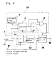
- Fig. 7 is a fifth example of the signal level detecting circuit 2, the difference with respect to the example up to the above description is that in the above described example, the output signal of the color image sensor 1 is saturated, and all the uniform control signals are adapted to be generated, while in the present embodiment, the control signal corresponding to the condition of the saturation signal is adapted to be generated.
- the signal from the color image sensor 1 is inputted to the input terminal 7 as shown in Fig. 7, and the signal is detected as to whether or not the saturation of the signal from the color image sensor 1 exists by the saturation detecting circuit 36 using the construction the same as the circuit shown in Fig. 4 (a).
- the signal to be inputted to the input terminal 7 is guided even into the third 1 picture element delaying circuit 31 and is delayed by one picture element, and the smaller signal of the signal not delayed or the signal delayed by one picture lement is selected by the selecting circuit 32.
- the output signal of the selecting circuit 32 is guided into the switching circuit 33.
- the vertical sharpness setting control signal for setting the vertical sharpness emphasis when the signal of the color image sensor 1 is not saturated is inputted into the other input terminal 34 of the switching circuit 33.
- the two input signals are switched with the control signal from the saturation detecting circuit 36 and are outputted into the output terminal 35.
- the saturation detecting circuit 36 does not detect the saturation of the signal, the vertical sharpness setting control signal is outputted into the output terminal 35.
- the control amount from the vertical sharpness correcting signal generating circuit 3 is set so as to emphasize the vertical sharpness.
- the saturation detecting circuit 36 detects the saturation of the signal, the output signal of the selecting circuit 32 is outputted to the output terminal 35.
- the output signal of the output terminal 35 will be described further with the use of Fig. 8.
- the solid straight lines (a) and (b) of Fig. 8 show the straight lines (a) and (b) of Fig. 20 and show the output signal level with respect to the incident light amount of two picture elements of one horizontal line of the color image sensor 1.
- the curve line (c) of Fig. 8 shows the output signal of the output terminal 35, namely, the vertical sharpness controlling signal. It is the value of the vertical sharpness setting control signal level while the incident light quantity where signal of the color image sensor 1 is not saturated is smaller than L1, the level becomes the signal level corresponding to the signal (Fig. 8, the curve line (b)) of the picture element not saturated when the signal of the color image sensor 1 starts its saturation.
- the value of the vertical sharpness control signal is made smaller when the signal level of the picture element not saturated is smaller, and the value of the vertical sharpness control signal is made larger when the signal level of the picture element not saturated is larger so as to effect the controlling operation of respectively decreasing or increasing the emphasis of the vertical sharpness.
- the signal level difference between the horizontal lines when the signal has been saturated is also large when the signal level difference between the picture elements are generally large.
- the signal level difference between the picture elements is small, the signal level difference between the horizontal lines when the signal has been saturated is also small, with an advantage that the conventional problem points may be reduced without making the signal level difference between the horizontal lines conspicuous or without the unnecessary deterioration of the vertical sharpness.
- the saturation detecting circuit 36 to be used in the above described example is not necessary to be restricted to the above described circuit example. It is clear that the circuit construction of the Fig. 4 (b), Fig. 6 (a), (b) which are in the above described second, third, fourth examples of the above described signal level detecting circuit 2 may be used.
- the signal of the line to be saturated is required to be guided into the selecting circuit 32 when the example where the saturation detecting signal is adapted to be caused when the signal is saturated even in either line of adjacent two lines with the use of the 1H delaying circuit as in the example of Fig. 6 (a), (b). Such example is shown in Fig. 9 and Fig. 10.
- Fig. 9 is a first detailed construction example of the fifth signal level detecting circuit, where the circuit of Fig. 6 (a) is used in the signal level detecting circuit 2 of the example of Fig. 7 so as to effect small modifications.
- the saturation detecting signal of two signals, the signal through the 1H delaying circuit and the signal not delayed by the 1H delaying circuit are fed into the control terminals a, b independently as the control signal into the selecting circuit 51 from the saturation detecting circuit 36.
- the signal passing through the 1H delaying circuit, the signal not passing through the 1H delaying circuit, the vertical sharpness setting control signal are respectively guided into three input terminals c, d, e of the selecting circuit 51.
- the selecting circuit 51 selects the signal of the input terminal d when the control input of the control terminal b is high at level, the signal of the input terminal c when the control input of the control terminal a is high at level, the signal of the input terminal e when the control input of the control terminals a and b are both low at level, the input terminal c or d (although the smaller signal of the input terminals c, d may be ideally selected, either of two signals may be selected) when the control inputs of the control terminals a and b are both high at level.
- the output signal of the selecting circuit 51 is guided into the 1 picture element delaying circuit 53 and the small signal selecting circuit 54.
- the signal corresponding to the signal level of the picture element not saturated of the saturated horizontal line or (when the signal is not saturated) the vertical sharpness setting control signal is outputted into the output terminal 55, with effects the same as in the example of Fig. 7 being obtained.
- the 1 picture element delaying circuit and the small signal selecting circuit may be omitted by one respectively by the application of the circuit of Fig. 6 (a) as it is into Fig. 7.
- Fig. 10 is a second detailed construction example of the fifth signal level detecting circuit, where the circuit of Fig. 6 (b) is used in the signal level detecting circuit 2 of Fig. 7, further the output signal of the 1H delaying circuit 20, and the signal, where the signal delayed further by the second 1H delaying circuit 42, and the original input signal (signal not delayed) are averaged by the adding circuit 43 and X 1/2 circuit 44, are used as input signals.
- the vertical sharpness correcting signal may be controlled by the signal condition of all the adjacent three lines including the line of the horizontal lines for obtaining the luminance signal, so that the control operation may be effected more correctly and the signal level difference caused between the lines may be controlled to minimum.
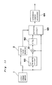
- Fig. 11 is a block diagram of a first embodiment of the second invention.
- the difference with respect to the first invention of Fig. 1 is in that the signal level difference between the horizontal lines is corrected by the controlling operation of the vertical sharpness correcting signal when the saturation of the signal has been caused in the first invention, while the signal level difference between the horizontal lines is adapted to be removed, so that the luminance signal may be obtained from the average signal of the signals of the adjacent two lines when the saturation of the signal has been caused in the second invention.
- the signal where the signal level difference between the horizontal lines by the saturation of the signal is outputted as shown in Fig. 13, the wave form (a) as described in the paragraph of the first invention from the color image sensor 1 in Fig. 11.
- the signal is guided into the signal level detecting circuit 2 which is the same as that used in the first invention, so that the saturation condition of the signal similar to that in the first invention is detected.
- the signal from the color image sensor 1 is guided into one input terminal of the switching circuit 63.
- This signal, and the signal (namely, average signal of two adjacent lines) where the signal (Fig. 13, the wave form (a)) delayed by 1H by the 1H delaying circuit 60 and the signal not delayed (Fig.
- the wave form (b)) are averaged by the adding circuit 61 and the X1/2 circuit 62 are switched by the control signal from the signal level detecting circuit 2 and is guided into the luminance signal processing circuit 64.
- the switching circuit 63 selects and outputs the signal from the color image sensor 1 when the saturation of the signal is not caused, and selects and outputs the average signal of two lines when the saturation of the signal is caused. Therefore, the luminance signal good in the vertical resolution for each of the respective horizontal lines will be the output of the luminance signal processing circuit 64 when the saturation of the signal is not caused.
- the saturation of the signal is caused, the signal where the signal level difference between the lines are corrected.
- the signal from the color image sensor 1 is a signal shown in Fig.
- the wave form (c) is the output signal when the signal level detecting circuit (2) is adapted to generate the control signal corresponding to the saturation condition of the signal of the one horizontal line as in the example of Fig. 4 (a), (b), and the signal level difference dS between the lines is reduced into 1/2.
- the wave form (c)' is the output signal when the signal level detecting circuit is adapted to generate the control signal corresponding to the saturation condition of the signal of two horizontal lines as shown in the example of Fig. 6 (a), (b), and the signal level difference between the lines are corrected into zero.
- Fig. 12 is a block diagram of a second embodiment of the second invention, is an example where the 1H delaying circuit within the signal level detecting circuit 65 is adapted to be omitted when the signal level detecting circuit 65 is adapted to generate the control signal corresponding to the saturation condition of the signals of two horizontal lines as the construction where the output of the X 1 / 2 circuits 62 of the first embodiment of the second invention of Fig. 1, namely, the average signal of the adjacent two lines are adapted to be also guided into the signal level detecting circuit 65.
- the output of the X 1 / 2 circuit 62 is adapted to be guided into the signal level detecting circuit 65 in the embodiment
- the output of the 1H delaying circuit 60 may be, needless to say, constructed to be guided into the signal level detecting circuit 65.
- the switching circuit 63 basically effects the on ⁇ off control in the second invention of the present invention of the above described Fig. 11 and Fig. 12, such saturation detecting circuit as in Fig. (a), (b) or Fig. 6 (a), (b) is proper in the signal level detecting circuit.
- the vertical sharpness correcting circuit may be included in the interior of the luminance signal processing circuit 64, the vertical sharpness correction signal generating circuit may be provided in addition so that the vertical sharpness correcting operation may be effected with the output of the luminance signal processing circuit 64.
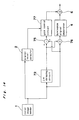
- Fig. 14 is a block diagram of a first embodiment of the third invention, in the difference between the first invention of Fig. 1 and the second invention of Fig. 11, as the first invention generates the luminance signal from one signal line, the vertical resolution is good, but the signal having the signal level difference is obtained between the lines when the saturation of the signal has been caused, the signal level difference between the signal horizontal lines is corrected by the controlling of the vertical sharpness correcting signal when the saturation has been caused. Also, in the second invention, the luminance signal is adapted to be obtained from the average signal of the adjacent second lines when the saturation of the signal has been caused, so that the signal level difference between the horizontal lines are adapted to be removed.
- the luminance signal is adapted to be obtained from the average signal of the signals of the adjacent two lines of signals or the weighted average signal of the signals of the adjacent three lines of signals by the combination of the above described first and second inventions, so that the luminance signal good at the vertical resolution is obtained when the saturation of the signal has not been caused by the addition of the vertical sharpness correcting signal controlled by the signal level detecting circuit output upon the signal, the luminance signal corrected in the signal level difference between the lines may be obtained when the saturation of the signal has been caused.
- the signal from the color image sensor 1 is detected at the level of the signal by the signal level detecting circuit 2 as in the embodiment of the invention given so far, and the control signal corresponding to the condition of the signal is outputted. Therefore, the construction of Fig. 7, Fig. 9, Fig. 10 is suitable as the signal level detecting circuit 2.
- the signal from the color image sensor 1 is guided into the 1H delaying circuit 72, and the signal delayed by 1H and the signal not delayed are guided into the adding circuit 76 and the subtracting circuit 75.
- the output signal of the adding circuit 76 becomes the average signal of the adjacent two lines, is guided into the luminance signal separating circuit 4, so that the main luminance signal is obtained.
- the signal is not caused in the signal level difference between the lines even when the signal has been saturated, but is not normally good in the vertical sharpness.
- the output signal of the subtracting circuit 75 is the difference signal, namely, the vertical edge signal of adjacent two lines, and therefore, becomes the signal for vertical sharpness correcting use.
- the output signal of the subtracting circuit 75 is gain controlled with the control signal from the signal level detecting circuit 2 by the gain control circuit 77.
- the output of the gain control circuit 77 is added, to the main luminance signal from the luminance signal separating circuit 4 by the adding circuit 6.
- the gain control circuit 77 controls the gain of the vertical sharpness correcting signal so that the vertical sharpness may be established into the desired value when the signal has not been saturated, and so that the gain of the vertical sharpness correcting signal may be controlled in accordance with the saturation level when the saturation of the signal is caused. Therefore, in the output of the adding circuit 6, the luminance signal good in the vertical resolution for each of the respective horizontal lines when the saturation of the signal has not been caused is obtained. The signal corrected in the signal level difference between the lines is obtained when the saturation of the signal has been caused is obtained.
- Fig. 15 is a block diagram of the second embodiment of the third invention.
- the difference with respect to the first embodiment of the third invention of Fig. 14 is in that the signal to be guided to the adding circuit 76 and the subtracting circuit 76 is turned into a first signal with the output signal of the color image sensor 1 being delayed by 1H by the 1H delaying circuit 71, and into a second signal wherein the output signal of the color image sensor 1 and the signal which has delayed the output signal of the 1H delaying circuit 71 by 1H further by the 1H delaying circuit 72 are averaged by the adding circuit 73 and X 1 / 2 circuit 74.
- the luminance signal and the vertical sharpness correcting signal may be fundamentally obtained from the adjacent three lines, further the vertical sharpness correcting signal may be controlled by all the three line signal condition, and the continuous control may be effected more correctly for each of the lines, so that the luminance signal which is gentle, smaller in the deterioration of the vertical sharpness, and smaller in the signal level difference caused among the lines.
- the output signal of the 1H delaying circuit 72 in Fig. 14 and Fig. 15, as in the embodiment of the Fig. 12, the output signal of the 1H delaying circuit 72 in Fig. 14, the output signal of the X 1 / 2 circuit 74 in Fig. 15, or the output signal of the 1H delaying circuit 71 and the 1H delaying circuit 72 are adapted to be also guided into the signal level detecting circuit 65 of Fig 12.
- the signal level detecting circuit 65 is adapted to generate the control signal corresponding to the saturation condition of the two horizontal line signal, it is clear that 1H delaying circuit within the signal level detecting circuit 65 is adapted to be omitted.
- the analog processing digital processing has not been referred to as the signal processing system in the description of the embodiment of the above described present invention, it is clear that the present invention may be achieved even in any processing system.
- the signal level detection circuit in the above described embodiment is proper to detect the signal level for each of the picture elements, the digital processing is easier to realize.
- the processing for converting the output signal of the color image sensor 1 into the digital signal by the A/D converting circuit becomes necessary in all the above described embodiments.
- the present invention is not restricted to the color image sensor 1 with the color filters shown in Fig. 2 being arranged. It is clear that the present invention may be applied to the general color image sensor on which the color filters are arranged, which are adapted to output the information from the object to be photographed as the different color signals for each of the horizontal lines.
Landscapes
- Engineering & Computer Science (AREA)
- Multimedia (AREA)
- Signal Processing (AREA)
- Physics & Mathematics (AREA)
- Spectroscopy & Molecular Physics (AREA)
- Color Television Image Signal Generators (AREA)
- Transforming Light Signals Into Electric Signals (AREA)
Applications Claiming Priority (2)
| Application Number | Priority Date | Filing Date | Title |
|---|---|---|---|
| JP153656/90 | 1990-06-12 | ||
| JP2153656A JP2722784B2 (ja) | 1990-06-12 | 1990-06-12 | カラー撮像装置 |
Publications (3)
| Publication Number | Publication Date |
|---|---|
| EP0461615A2 true EP0461615A2 (fr) | 1991-12-18 |
| EP0461615A3 EP0461615A3 (en) | 1992-03-04 |
| EP0461615B1 EP0461615B1 (fr) | 1996-05-08 |
Family
ID=15567306
Family Applications (1)
| Application Number | Title | Priority Date | Filing Date |
|---|---|---|---|
| EP91109567A Expired - Lifetime EP0461615B1 (fr) | 1990-06-12 | 1991-06-11 | Appareil de prise de vues en couleurs |
Country Status (4)
| Country | Link |
|---|---|
| US (1) | US5144399A (fr) |
| EP (1) | EP0461615B1 (fr) |
| JP (1) | JP2722784B2 (fr) |
| DE (1) | DE69119300T2 (fr) |
Cited By (1)
| Publication number | Priority date | Publication date | Assignee | Title |
|---|---|---|---|---|
| WO1998018263A3 (fr) * | 1996-10-21 | 1998-06-18 | Philips Electronics Nv | Amelioration de la finesse |
Families Citing this family (10)
| Publication number | Priority date | Publication date | Assignee | Title |
|---|---|---|---|---|
| JP2752288B2 (ja) * | 1992-02-28 | 1998-05-18 | 三洋電機株式会社 | ディジタルビデオカメラ |
| JP3196354B2 (ja) * | 1992-10-13 | 2001-08-06 | 株式会社日立製作所 | 輪郭補正回路及び撮像装置 |
| JPH06327628A (ja) * | 1993-05-20 | 1994-11-29 | Fuji Photo Optical Co Ltd | 同時式電子内視鏡装置の信号処理回路 |
| US5841491A (en) * | 1993-10-14 | 1998-11-24 | Envision Medical Corp. | Fiberscope enhancement system |
| JP3076810B2 (ja) * | 1994-01-20 | 2000-08-14 | モトローラ株式会社 | 垂直輪郭補正回路 |
| JPH07226956A (ja) * | 1994-02-09 | 1995-08-22 | Nippon Motorola Ltd | 輝度信号色信号分離回路 |
| US5811857A (en) * | 1996-10-22 | 1998-09-22 | International Business Machines Corporation | Silicon-on-insulator body-coupled gated diode for electrostatic discharge (ESD) and analog applications |
| DE69838779D1 (de) | 1997-08-26 | 2008-01-10 | Matsushita Electric Industrial Co Ltd | Korrekturvorrichtung für senkrechte konturen |
| EP1148735A1 (fr) | 2000-04-20 | 2001-10-24 | Koninklijke Philips Electronics N.V. | Caméra avec filtre couleur |
| JP4743839B2 (ja) * | 2005-02-15 | 2011-08-10 | キヤノン株式会社 | 撮像装置 |
Family Cites Families (6)
| Publication number | Priority date | Publication date | Assignee | Title |
|---|---|---|---|---|
| DE3381818D1 (de) * | 1982-12-14 | 1990-09-20 | Matsushita Electric Industrial Co Ltd | Festkoerper-farbabbildungsanordnung. |
| JPS60171887A (ja) * | 1984-02-15 | 1985-09-05 | Matsushita Electric Ind Co Ltd | 固体カラ−撮像装置 |
| JPS63105591A (ja) * | 1986-10-22 | 1988-05-10 | Sony Corp | ビデオカメラ |
| JP2581070B2 (ja) * | 1987-04-28 | 1997-02-12 | ソニー株式会社 | 撮像信号処理装置 |
| JPS63279691A (ja) * | 1987-05-11 | 1988-11-16 | Mitsubishi Electric Corp | 垂直輪郭補正回路 |
| US4903121A (en) * | 1987-05-14 | 1990-02-20 | Matsushita Electric Industrial Co., Ltd. | Image pick up apparatus having pixel compensation circuit |
-
1990
- 1990-06-12 JP JP2153656A patent/JP2722784B2/ja not_active Expired - Lifetime
-
1991
- 1991-06-11 DE DE69119300T patent/DE69119300T2/de not_active Expired - Fee Related
- 1991-06-11 EP EP91109567A patent/EP0461615B1/fr not_active Expired - Lifetime
- 1991-06-11 US US07/713,154 patent/US5144399A/en not_active Expired - Lifetime
Cited By (1)
| Publication number | Priority date | Publication date | Assignee | Title |
|---|---|---|---|---|
| WO1998018263A3 (fr) * | 1996-10-21 | 1998-06-18 | Philips Electronics Nv | Amelioration de la finesse |
Also Published As
| Publication number | Publication date |
|---|---|
| DE69119300D1 (de) | 1996-06-13 |
| EP0461615B1 (fr) | 1996-05-08 |
| EP0461615A3 (en) | 1992-03-04 |
| DE69119300T2 (de) | 1997-01-02 |
| JP2722784B2 (ja) | 1998-03-09 |
| JPH0445686A (ja) | 1992-02-14 |
| US5144399A (en) | 1992-09-01 |
Similar Documents
| Publication | Publication Date | Title |
|---|---|---|
| US6593970B1 (en) | Imaging apparatus with dynamic range expanded, a video camera including the same, and a method of generating a dynamic range expanded video signal | |
| KR100433111B1 (ko) | 비디오신호아웃라인강조장치및방법 | |
| EP0430982A4 (en) | Wide dynamic range camera | |
| JPH0335870B2 (fr) | ||
| EP0823814B1 (fr) | Circuit de mixage d'images | |
| KR20030014703A (ko) | 윤곽 강조 장치 | |
| US5767900A (en) | Digital apparatus for contour enhancement of video signal | |
| US5144399A (en) | Color image pickup apparatus | |
| KR930003572B1 (ko) | 전자적으로 확대 촬영 가능한 촬상 장치 | |
| JP2751447B2 (ja) | ノイズ低減装置 | |
| JP3748031B2 (ja) | 映像信号処理装置及び映像信号処理方法 | |
| JP4175587B2 (ja) | 画像処理装置及びその方法、撮像装置、並びにメモリ媒体 | |
| JP2893914B2 (ja) | カラー撮像装置 | |
| JP3743055B2 (ja) | 画像の輪郭強調方法および装置 | |
| JP2698404B2 (ja) | 輝度信号処理装置 | |
| JPH06245106A (ja) | 撮像装置 | |
| JPH0851634A (ja) | テレビジョンカメラ装置 | |
| JP2698406B2 (ja) | 撮像装置 | |
| JPH05244462A (ja) | 映像信号処理装置 | |
| JPH0662278A (ja) | 映像信号処理装置 | |
| JPH04280579A (ja) | 撮像信号処理装置におけるスミア補正回路 | |
| JP2000032479A (ja) | 映像信号処理装置及び映像信号処理方法 | |
| JPH05145796A (ja) | 映像信号処理装置 | |
| JPH04281670A (ja) | 画像読取装置および画像読取方式 | |
| JPH05153613A (ja) | 映像信号処理装置 |
Legal Events
| Date | Code | Title | Description |
|---|---|---|---|
| PUAI | Public reference made under article 153(3) epc to a published international application that has entered the european phase |
Free format text: ORIGINAL CODE: 0009012 |
|
| 17P | Request for examination filed |
Effective date: 19910611 |
|
| AK | Designated contracting states |
Kind code of ref document: A2 Designated state(s): DE FR GB |
|
| PUAL | Search report despatched |
Free format text: ORIGINAL CODE: 0009013 |
|
| AK | Designated contracting states |
Kind code of ref document: A3 Designated state(s): DE FR GB |
|
| 17Q | First examination report despatched |
Effective date: 19940317 |
|
| GRAH | Despatch of communication of intention to grant a patent |
Free format text: ORIGINAL CODE: EPIDOS IGRA |
|
| GRAA | (expected) grant |
Free format text: ORIGINAL CODE: 0009210 |
|
| AK | Designated contracting states |
Kind code of ref document: B1 Designated state(s): DE FR GB |
|
| REF | Corresponds to: |
Ref document number: 69119300 Country of ref document: DE Date of ref document: 19960613 |
|
| ET | Fr: translation filed | ||
| PLBE | No opposition filed within time limit |
Free format text: ORIGINAL CODE: 0009261 |
|
| STAA | Information on the status of an ep patent application or granted ep patent |
Free format text: STATUS: NO OPPOSITION FILED WITHIN TIME LIMIT |
|
| 26N | No opposition filed | ||
| REG | Reference to a national code |
Ref country code: GB Ref legal event code: IF02 |
|
| PGFP | Annual fee paid to national office [announced via postgrant information from national office to epo] |
Ref country code: DE Payment date: 20080619 Year of fee payment: 18 |
|
| PGFP | Annual fee paid to national office [announced via postgrant information from national office to epo] |
Ref country code: FR Payment date: 20080617 Year of fee payment: 18 |
|
| PGFP | Annual fee paid to national office [announced via postgrant information from national office to epo] |
Ref country code: GB Payment date: 20080611 Year of fee payment: 18 |
|
| GBPC | Gb: european patent ceased through non-payment of renewal fee |
Effective date: 20090611 |
|
| REG | Reference to a national code |
Ref country code: FR Ref legal event code: ST Effective date: 20100226 |
|
| PG25 | Lapsed in a contracting state [announced via postgrant information from national office to epo] |
Ref country code: FR Free format text: LAPSE BECAUSE OF NON-PAYMENT OF DUE FEES Effective date: 20090630 |
|
| PG25 | Lapsed in a contracting state [announced via postgrant information from national office to epo] |
Ref country code: GB Free format text: LAPSE BECAUSE OF NON-PAYMENT OF DUE FEES Effective date: 20090611 |
|
| PG25 | Lapsed in a contracting state [announced via postgrant information from national office to epo] |
Ref country code: DE Free format text: LAPSE BECAUSE OF NON-PAYMENT OF DUE FEES Effective date: 20100101 |