EP0462596A1 - Verfahren und Einrichtung für die Verpackung eines Halbleiterkomponenten - Google Patents
Verfahren und Einrichtung für die Verpackung eines Halbleiterkomponenten Download PDFInfo
- Publication number
- EP0462596A1 EP0462596A1 EP91110072A EP91110072A EP0462596A1 EP 0462596 A1 EP0462596 A1 EP 0462596A1 EP 91110072 A EP91110072 A EP 91110072A EP 91110072 A EP91110072 A EP 91110072A EP 0462596 A1 EP0462596 A1 EP 0462596A1
- Authority
- EP
- European Patent Office
- Prior art keywords
- light
- substrate
- plane
- semiconductor device
- bonding head
- Prior art date
- Legal status (The legal status is an assumption and is not a legal conclusion. Google has not performed a legal analysis and makes no representation as to the accuracy of the status listed.)
- Withdrawn
Links
Images


Classifications
-
- H—ELECTRICITY
- H10—SEMICONDUCTOR DEVICES; ELECTRIC SOLID-STATE DEVICES NOT OTHERWISE PROVIDED FOR
- H10P—GENERIC PROCESSES OR APPARATUS FOR THE MANUFACTURE OR TREATMENT OF DEVICES COVERED BY CLASS H10
- H10P72/00—Handling or holding of wafers, substrates or devices during manufacture or treatment thereof
- H10P72/04—Apparatus for manufacture or treatment
- H10P72/0446—Apparatus for mounting on conductive members, e.g. leadframes or conductors on insulating substrates
-
- H—ELECTRICITY
- H10—SEMICONDUCTOR DEVICES; ELECTRIC SOLID-STATE DEVICES NOT OTHERWISE PROVIDED FOR
- H10P—GENERIC PROCESSES OR APPARATUS FOR THE MANUFACTURE OR TREATMENT OF DEVICES COVERED BY CLASS H10
- H10P72/00—Handling or holding of wafers, substrates or devices during manufacture or treatment thereof
- H10P72/50—Handling or holding of wafers, substrates or devices during manufacture or treatment thereof for positioning, orientation or alignment
- H10P72/53—Handling or holding of wafers, substrates or devices during manufacture or treatment thereof for positioning, orientation or alignment using optical controlling means
-
- H—ELECTRICITY
- H10—SEMICONDUCTOR DEVICES; ELECTRIC SOLID-STATE DEVICES NOT OTHERWISE PROVIDED FOR
- H10W—GENERIC PACKAGES, INTERCONNECTIONS, CONNECTORS OR OTHER CONSTRUCTIONAL DETAILS OF DEVICES COVERED BY CLASS H10
- H10W72/00—Interconnections or connectors in packages
- H10W72/071—Connecting or disconnecting
- H10W72/072—Connecting or disconnecting of bump connectors
-
- H—ELECTRICITY
- H10—SEMICONDUCTOR DEVICES; ELECTRIC SOLID-STATE DEVICES NOT OTHERWISE PROVIDED FOR
- H10W—GENERIC PACKAGES, INTERCONNECTIONS, CONNECTORS OR OTHER CONSTRUCTIONAL DETAILS OF DEVICES COVERED BY CLASS H10
- H10W72/00—Interconnections or connectors in packages
- H10W72/071—Connecting or disconnecting
- H10W72/0711—Apparatus therefor
-
- H—ELECTRICITY
- H10—SEMICONDUCTOR DEVICES; ELECTRIC SOLID-STATE DEVICES NOT OTHERWISE PROVIDED FOR
- H10W—GENERIC PACKAGES, INTERCONNECTIONS, CONNECTORS OR OTHER CONSTRUCTIONAL DETAILS OF DEVICES COVERED BY CLASS H10
- H10W72/00—Interconnections or connectors in packages
- H10W72/071—Connecting or disconnecting
- H10W72/0711—Apparatus therefor
- H10W72/07173—Means for moving chips, wafers or other parts, e.g. conveyor belts
-
- H—ELECTRICITY
- H10—SEMICONDUCTOR DEVICES; ELECTRIC SOLID-STATE DEVICES NOT OTHERWISE PROVIDED FOR
- H10W—GENERIC PACKAGES, INTERCONNECTIONS, CONNECTORS OR OTHER CONSTRUCTIONAL DETAILS OF DEVICES COVERED BY CLASS H10
- H10W72/00—Interconnections or connectors in packages
- H10W72/071—Connecting or disconnecting
- H10W72/0711—Apparatus therefor
- H10W72/07178—Means for aligning
-
- H—ELECTRICITY
- H10—SEMICONDUCTOR DEVICES; ELECTRIC SOLID-STATE DEVICES NOT OTHERWISE PROVIDED FOR
- H10W—GENERIC PACKAGES, INTERCONNECTIONS, CONNECTORS OR OTHER CONSTRUCTIONAL DETAILS OF DEVICES COVERED BY CLASS H10
- H10W72/00—Interconnections or connectors in packages
- H10W72/071—Connecting or disconnecting
- H10W72/072—Connecting or disconnecting of bump connectors
- H10W72/07221—Aligning
- H10W72/07223—Active alignment, e.g. using optical alignment using marks or sensors
-
- H—ELECTRICITY
- H10—SEMICONDUCTOR DEVICES; ELECTRIC SOLID-STATE DEVICES NOT OTHERWISE PROVIDED FOR
- H10W—GENERIC PACKAGES, INTERCONNECTIONS, CONNECTORS OR OTHER CONSTRUCTIONAL DETAILS OF DEVICES COVERED BY CLASS H10
- H10W72/00—Interconnections or connectors in packages
- H10W72/071—Connecting or disconnecting
- H10W72/072—Connecting or disconnecting of bump connectors
- H10W72/07231—Techniques
- H10W72/07236—Soldering or alloying
-
- H—ELECTRICITY
- H10—SEMICONDUCTOR DEVICES; ELECTRIC SOLID-STATE DEVICES NOT OTHERWISE PROVIDED FOR
- H10W—GENERIC PACKAGES, INTERCONNECTIONS, CONNECTORS OR OTHER CONSTRUCTIONAL DETAILS OF DEVICES COVERED BY CLASS H10
- H10W72/00—Interconnections or connectors in packages
- H10W72/071—Connecting or disconnecting
- H10W72/072—Connecting or disconnecting of bump connectors
- H10W72/07251—Connecting or disconnecting of bump connectors characterised by changes in properties of the bump connectors during connecting
-
- H—ELECTRICITY
- H10—SEMICONDUCTOR DEVICES; ELECTRIC SOLID-STATE DEVICES NOT OTHERWISE PROVIDED FOR
- H10W—GENERIC PACKAGES, INTERCONNECTIONS, CONNECTORS OR OTHER CONSTRUCTIONAL DETAILS OF DEVICES COVERED BY CLASS H10
- H10W72/00—Interconnections or connectors in packages
- H10W72/20—Bump connectors, e.g. solder bumps or copper pillars; Dummy bumps; Thermal bumps
-
- Y—GENERAL TAGGING OF NEW TECHNOLOGICAL DEVELOPMENTS; GENERAL TAGGING OF CROSS-SECTIONAL TECHNOLOGIES SPANNING OVER SEVERAL SECTIONS OF THE IPC; TECHNICAL SUBJECTS COVERED BY FORMER USPC CROSS-REFERENCE ART COLLECTIONS [XRACs] AND DIGESTS
- Y10—TECHNICAL SUBJECTS COVERED BY FORMER USPC
- Y10T—TECHNICAL SUBJECTS COVERED BY FORMER US CLASSIFICATION
- Y10T29/00—Metal working
- Y10T29/49—Method of mechanical manufacture
- Y10T29/49002—Electrical device making
- Y10T29/49117—Conductor or circuit manufacturing
- Y10T29/49124—On flat or curved insulated base, e.g., printed circuit, etc.
- Y10T29/4913—Assembling to base an electrical component, e.g., capacitor, etc.
- Y10T29/49131—Assembling to base an electrical component, e.g., capacitor, etc. by utilizing optical sighting device
-
- Y—GENERAL TAGGING OF NEW TECHNOLOGICAL DEVELOPMENTS; GENERAL TAGGING OF CROSS-SECTIONAL TECHNOLOGIES SPANNING OVER SEVERAL SECTIONS OF THE IPC; TECHNICAL SUBJECTS COVERED BY FORMER USPC CROSS-REFERENCE ART COLLECTIONS [XRACs] AND DIGESTS
- Y10—TECHNICAL SUBJECTS COVERED BY FORMER USPC
- Y10T—TECHNICAL SUBJECTS COVERED BY FORMER US CLASSIFICATION
- Y10T29/00—Metal working
- Y10T29/53—Means to assemble or disassemble
- Y10T29/53087—Means to assemble or disassemble with signal, scale, illuminator, or optical viewer
- Y10T29/53091—Means to assemble or disassemble with signal, scale, illuminator, or optical viewer for work-holder for assembly or disassembly
-
- Y—GENERAL TAGGING OF NEW TECHNOLOGICAL DEVELOPMENTS; GENERAL TAGGING OF CROSS-SECTIONAL TECHNOLOGIES SPANNING OVER SEVERAL SECTIONS OF THE IPC; TECHNICAL SUBJECTS COVERED BY FORMER USPC CROSS-REFERENCE ART COLLECTIONS [XRACs] AND DIGESTS
- Y10—TECHNICAL SUBJECTS COVERED BY FORMER USPC
- Y10T—TECHNICAL SUBJECTS COVERED BY FORMER US CLASSIFICATION
- Y10T29/00—Metal working
- Y10T29/53—Means to assemble or disassemble
- Y10T29/5313—Means to assemble electrical device
- Y10T29/53174—Means to fasten electrical component to wiring board, base, or substrate
-
- Y—GENERAL TAGGING OF NEW TECHNOLOGICAL DEVELOPMENTS; GENERAL TAGGING OF CROSS-SECTIONAL TECHNOLOGIES SPANNING OVER SEVERAL SECTIONS OF THE IPC; TECHNICAL SUBJECTS COVERED BY FORMER USPC CROSS-REFERENCE ART COLLECTIONS [XRACs] AND DIGESTS
- Y10—TECHNICAL SUBJECTS COVERED BY FORMER USPC
- Y10T—TECHNICAL SUBJECTS COVERED BY FORMER US CLASSIFICATION
- Y10T29/00—Metal working
- Y10T29/53—Means to assemble or disassemble
- Y10T29/5313—Means to assemble electrical device
- Y10T29/53191—Means to apply vacuum directly to position or hold work part
Definitions
- the present invention relates to a method and apparatus for packaging a semiconductor device, and more particularly to a method and apparatus for packaging a semiconductor device to a substrate by face-down bonding.
- a flip chip packaging technique in the face-down bonding has recently been attracting interest in view of a packaging density and workability in packaging a semiconductor device onto a substrate. This method is described in an article entitled “Technology Trend of Flip Chip Packaging " Electronic Packaging Technology, December 1989.
- the face-down bonding is carried out without adjustment after an initial adjustment of the packaging apparatus to adjust a parallelism between a bonding head and the plane of the substrate.
- the semiconductor device may not be bonded to the plane of the substrate without failure.
- the semiconductor device is observed by a TV camera mounted beside a bonding head which sucks and holds the semiconductor device during the face-down bonding process to watch the parallelism between the bonding head and the substrate.
- the present invention intends to solve the above problem and provide a semiconductor device packaging apparatus which can comply with the high density packaging.
- It is an object of the present invention to provide an apparatus for packaging a semiconductor device comprising: bonding head having a holding plane adapted to hold a semiconductor device having a bump electrode formed on a front surface thereof by sucking a rear surface thereof and a light reflective plane formed around the holding plane; a stage opposed to said holding plane adapted to hold a substrate on which the semiconductor device is to be face-down bonded; irradiation means for irradiating a coherent light to the light reflective plane and said stage; observing means for causing a light reflected by the light reflective plane to interfere with a light reflected by a the substrate held by said stage, of the light irradiated by said irradiating means, to observe an interference state therebetween to detect the inclination between the semiconductor chip against the substrate; and adjusting means for moving the bonding head against said stage to adjust parallelism between the plane on which the bump electrode of the sucked semiconductor device is formed and the plane of the substrate to which the semiconductor device is to be bonded and face-down bonding the semiconductor
- It is further object of the present invention to provide a method for packaging a semiconductor device comprising the steps of: holding a semiconductor device having a bump electrode formed on a front surface thereof by sucking a rear surface thereof to a sucking surface on a bonding head; irradiating a coherent light to a light reflective plane of the bonding head formed around the sucking surface and a light reflective substrate to which the semiconductor device is to be bonded and held on a stage disposed facing to the bonding head; interfering a light reflected by the substrate and a light reflected by the light reflective light plane, of the light irradiated in said irradiative step to detect an interference fringe; and moving the bonding head in accordance with a state of the interference fringe detected in said detection step, adjusting a parallelism between the plane on which the bump electrode of the sucked semiconductor device is formed and the plane of the substrate to which the semiconductor device is to be bonded and face-down bonding the semiconductor device to the substrate.
- the coherent light is irradiated from the back side of the substrate.
- the light reflected by the light reflection plane on the bonding head is interfered with the light reflected by the back side of the substrate so that the parallelism between the surface of the semiconductor device and the plane of the substrate is exactly detected.
- the bonding ahead is moved in accordance with the detection output so that the parallelism between the surface of the semiconductor device and the plane of the substrate is maintained.
- the coherent light is irradiated from the front side of the substrate.
- the light reflected by the light reflection plane on the bonding head is interfered with the light reflected by the front side of the substrate and reflected by the light reflection plane so that the parallelism between the surface of the semiconductor device and the plane of the substrate is exactly detected.
- the bonding head is moved in accordance with the detection output so that the parallelism between the surface of the semiconductor device and the plane of the substrate is maintained.
- Fig. 1 shows a semiconductor device packaging apparatus of a first embodiment according to the present invention, and is used for packaging a semiconductor device in a light transmission substrate.
- the semiconductor device packaging apparatus has a bonding head 2 which has a plane 2a( sucking plane) for sucking and securing a semiconductor device 1, formed at an end thereof.
- a throught-hole 2b connected to a vacuum pump 10 is formed at a center of the plane 2a.
- a mirror plane 2c (light reflection plane) which is parallel to a bump electrode plane of the semiconductor device which is to be vacuum-sucked to the sucking plane is formed around the sucking plane.
- the mirror plane 2c may be formed by embedding a member made of a highly light reflective material around the through-hole 2b and polishing it.
- a position adjusting unit 11 is mechanically connected to the bonding head 2.
- the bonding head 2 is movable along a Z direction which is perpendicular to a XY plane which corresponds to a semiconductor mount plane 3a of the light transmissive substrate 3 mounted on the packaging apparatus, and a also adjustable to a X axis and a Y axis which are parallel to the XY plane and define a plane which passes through a center of the through-hole 2b on the plane 2a, toward rotation angles Ox and Oy, respectively, by the position adjusting unit 11.
- a substrate holder 4 of the semiconductor device packaging apparatus has a through-hole 4a so that it can support the substrate 3 at the periphery thereof and permit the irradiation of the light from the bottom side of the substrate 3.
- the size of the through-hole 4a is preferably larger than the area of the mirror plane 2c formed on the bonding head 2.
- the substrate holder 4 further has a securing mechanism (not shown) for securing the light transmissive substrate 3 mounted thereon.
- a half-mirror 5 is arranged below the through-hole 4a of the substrate holder 4.
- the half-mirror 5 is fixed at an angle of inclination of 45 degrees to the back side 3b of the light transmissive substrate 3 which is secured to the substrate holder 4.
- a light source 6 such as a laser beam generator which irradiates a coherent and collimated light perpendicularly to the rear surface side 3b of the secured light transmissive substrate 3 is arranged below the half-mirror 5.
- a monitor 7 such as a microscope for observing an interference state of the light, more specifically an interference fringe is arranged beside the half-mirror 5.
- the microscope 7 is positioned on a line extending from the inclined plane of the half-mirror 5 perpendicularly to the direction of propagation of the collimated light emitted from the light source 6.
- the substrate 3 is secured to a predetermined position to cover the through-hole 4a of the substrate holder 4.
- the semiconductor device 1 is displaced such that the plan opposite to the bump electrode plane covers the through-hole 2b of the bonding head 2, and the semiconductor device 1 is vacuum-sucked by the vacuum pump 10 through the through-hole 2b so that it is sucked and held to the end of the bonding head 2.
- the light source 6 is energized to irradiate the laser beam to the rear side of the substrate 3 through the half-mirror 5.
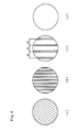
- the interference state between the light reflected by the rear surface 3b of the substrate 3 and the light reflected by the mirror plane 2c of the bonding head 2 is observed by the microscope 7. It the mirror plane 2c of the bonding head 2 substantially incline with respect to the semiconductor device mount plane 3a of the substrate 3, there are too many interference fringes to observe them, as shown in Fig. 4(a) using the position adjusting unit 11.
- the rotation angle Ox along the X axis and the rotation angle Oy along the Y axis of the bonding head 2 are adjusted to enable the observation of the interference fringes, as shown in Fig. 4(b).
- the rotation angle Ox along the X axis and the rotation angle Oy along the Y axis of the bonding head 2 are finely adjusted to expand an interval W of the observed interference fringes.
- the interference fringe disappears form a view field of the microscope 7, the adjustment of the angles of the bonding head 2 is stopped and the bonding head 2 is moved in the -Z direction (descending direction) to effect the face-down bonding.
- the observation area is 10mm on the mirror plane 2c of the bonding head 2 and a He-Ne laser beam having a wavelength of 0.63 ⁇ m is used as the coherent light
- an interference fringe appears at every optical path difference of 0.63 ⁇ m.
- the parallelism between the mirror plane 2c of the bonding head 2 and the semiconductor device mount plan 3a of the substrate 3 is smaller than 0.3 ⁇ m at the distance of 10mm, when the interference fringe is not observed as shown in Fig 4(d).
- the parallelism between the plane on which the bump electrode of the semiconductor device 1 is formed and the semiconductor device mount plane 3a of the substrate can be simply and precisely detected, and the inclination of the bonding head 2 is adjusted in accordance with the detection output so that the highly accurate face-down bonding is attained.
- Fig. 2 shows a semiconductor device packaging apparatus of a second embodiment according to the present invention and used for packaging a semiconductor device in a light substrate.
- the semiconductor device packaging apparatus has a bonding head 2 which has a plane 2a(sucking plane) for sucking and securing a semiconductor device 1, formed at an end thereof.
- a through-hole 2b connected to a vacuum pump 10 is formed at a center of the plane 2a.
- a mirror plane 2c(light reflection plane) which is parallel to a bump electrode plane of the semiconductor device which is to be vacuum-sucked to the sucking plan) is formed around the sucking plane.
- the mirror plane 2c may be formed by embedding a member made of a highly light reflective material around the through-hole 2b and polishing it.
- a position adjusting unit 11 is mechanically connected to the bonding head 2.
- the boning head 2 is movable along a Z direction which is perpendicular to a XY plane which correspond to a semiconductor mount plane 3a of a light reflective substrate 30 mounted on the packaging apparatus, and also adjustable to a X axis and a Y axis which are parallel to the XY plane and define a plane which passes through a center of the through-hole 2b on the plane 2a, toward rotation angles Ox and Oy, respectively, by the position adjusting unit 11.
- a substrate holder 4 of the semiconductor device packaging apparatus has a planer area to support the entire bottom surface of the substrate 3.
- the substrate holder 4 further has a securing mechanism (not shown) for securing the light reflective substrate 30 mounted thereon.
- An inclination measurement equipment 20 is arrange above the substrate support plane of the substrate holder 4.
- the inclination measurement equipment is mounted on a manual or automatic drive mechanism (not shown) so that it is movable between a first position which is between the bonding head 2 and the substrate holder 4, and a second position which is beyond the bonding head 2 or the substrate holders 4. It may be moved either by rotation or by parallel movement.
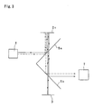
- the inclination measurement equipment 20 has a pair of half-mirrors 5a and 5b which are arranged to make angles of 45 degrees, respectively, with respect to the substrate support plane of the substrate holder 4 when the inclination measurement equipment 20 is at the first position.
- the half-mirrors 5a and 5b make an angle of 90 degrees to each other and the respective edges are connected.
- a light source 6 such as a laser beam generator which emits a coherent and collimated light at an angle of 45 degrees with respect to the plane of the half-mirror 5a is arranged beside the upper half-mirror 5a.
- a monitor 7 such as a microscope for observing an interference status of the light reflected by the half-mirror 5b, more specifically, an interference fringe is arranged beside the lower half-mirror 5b oppositely to the light source 6.
- the microscope 7 is arranged in a path of the collimated light emitted from the light source 6 to the half-mirror 5a to face the inclined plane of the half-mirror 5b.
- the light path thereof is shown in Fig. 3.
- the interference state between the broken line light and the solid line light shown in Fig. 3 can be observed through the microscope.
- the relative positions of the half-mirrors 5a and 5b, the light source 6 and the microscope 7 are fixed and they are moved integrally.
- the substrate 30 is secured to a position on the substrate holder 4 facing the bonding head 2.
- the semiconductor device 1 is disposed such that the opposite plane to the plane on which the bump electrode is formed covers the through-hole 2b of the bonding head 2, and the semiconductor device 1 is sucked and secured to the end of the bonding head 2 by the vacuum pump 10 through the through-hole 2b.
- the inclination measurement equipment 20 is fixed at the first position between the bonding head 2 and the substrate 30.
- the light source 6 is energized to irradiate the loser beam to the half-mirror 5a.
- the interference state between the light reflected by the front surface 3a of the substrate 3 and the light reflected by the mirror plane 2c of the bonding head 2 is observed through the microscope 7.
- the mirror plane 2c of the bonding head 2 substantially inclines to the semiconductor device mount plane 3a of the substrate 3, there are too many interference fringes to permit the observation of the interference fringes, as shown in Fig. 4(a).
- the rotation angle Ox along the X axis of the bonding head 2 are adjusted to enable the observation of the interference fringes, as shown in Fig. 4(b).
- the rotation angle Ox along the X axis and the rotation angle Oy along the Y axis of the bonding head 2 are finely adjusted to expand an interval w of the observed interference fringes.
- the interference fringe is no longer observed.
- the angle adjustment of the bonding head 2 is stopped and the angles of the bonding head 2 are fixed.
- the observation area is 10mm on the mirror plane 2c of the bonding head 2 and a He-Ne laser beam having a wavelength of 0.63 ⁇ m is used as the coherent light
- an interference fringe appears at every optical path difference of 0.63 ⁇ m. Accordingly, the parallelism between the mirror plane 2c of the bonding head 2 and the semiconductor device mount plane 3a of the substrate 30 is smaller than 0.3 ⁇ m at the distance of 10mm, when the interference fringe is not observed as shown in Fig. 4(d).
- the inclination measurement equipment 20 is moved to the second position beyond the area between bonding head 2 and the substrate 2. Then, the bonding head 2 is moved in the -Z direction (descending direction) and the face-down bonding is effected.
- the parallelism between the plane on which the bump electrode of the semiconductor device 1 is formed and the semiconductor device mount plane 3a of the substrate can be simply and precisely detected and the inclination of the bonding head 2 is adjusted in accordance with the detection output so that the highly accurate face-down bonding is attained.
- the present invention is not limited to the above embodiment but various modification thereof may be mode.
- the laser beam is used as the coherent light in the embodiment, any other coherent light may be used.
- the laser beam is not limited to the He-Ne laser beam.
- a light reflective member may be bonded instead.
- the parallelism between the semiconductor device and the substrate is detected by using the interference of the lights, as described above. Accordingly, the exact face-down bonding can be attained even for the semiconductor device having a fine bump.
Landscapes
- Wire Bonding (AREA)
- Length Measuring Devices By Optical Means (AREA)
Applications Claiming Priority (4)
| Application Number | Priority Date | Filing Date | Title |
|---|---|---|---|
| JP160346/90 | 1990-06-19 | ||
| JP2160346A JPH0451534A (ja) | 1990-06-19 | 1990-06-19 | 半導体素子実装方法 |
| JP178721/90 | 1990-07-06 | ||
| JP2178721A JPH0465844A (ja) | 1990-07-06 | 1990-07-06 | 半導体素子実装方法 |
Publications (1)
| Publication Number | Publication Date |
|---|---|
| EP0462596A1 true EP0462596A1 (de) | 1991-12-27 |
Family
ID=26486882
Family Applications (1)
| Application Number | Title | Priority Date | Filing Date |
|---|---|---|---|
| EP91110072A Withdrawn EP0462596A1 (de) | 1990-06-19 | 1991-06-19 | Verfahren und Einrichtung für die Verpackung eines Halbleiterkomponenten |
Country Status (4)
| Country | Link |
|---|---|
| US (1) | US5212880A (de) |
| EP (1) | EP0462596A1 (de) |
| KR (1) | KR950002186B1 (de) |
| CA (1) | CA2044649A1 (de) |
Cited By (24)
| Publication number | Priority date | Publication date | Assignee | Title |
|---|---|---|---|---|
| EP0569011A1 (de) * | 1992-05-06 | 1993-11-10 | Sumitomo Electric Industries, Limited | Verfahren zur Montierung eines Halbleiterchips und Anordnung |
| EP0570971A1 (de) * | 1992-05-22 | 1993-11-24 | Sumitomo Electric Industries, Limited | Flip-Chip-Bond Justiermarke |
| WO1998058403A1 (en) * | 1997-06-18 | 1998-12-23 | Micro Robotics Systems, Inc. | Method and apparatus for chip placement |
| EP0913857A1 (de) * | 1997-10-30 | 1999-05-06 | Esec Sa | Verfahren und Einrichtung für die Justierung des Bondkopfes eines Bonders, insbesondere eines Die-Bonders |
| US6031242A (en) * | 1998-01-23 | 2000-02-29 | Zevatech, Inc. | Semiconductor die in-flight registration and orientation method and apparatus |
| US6077022A (en) * | 1997-02-18 | 2000-06-20 | Zevatech Trading Ag | Placement machine and a method to control a placement machine |
| US6129040A (en) * | 1997-09-05 | 2000-10-10 | Esec Sa | Semi-conductor mounting apparatus for applying adhesive to a substrate |
| US6135339A (en) * | 1998-01-26 | 2000-10-24 | Esec Sa | Ultrasonic transducer with a flange for mounting on an ultrasonic welding device, in particular on a wire bonder |
| US6157870A (en) * | 1997-02-18 | 2000-12-05 | Zevatech Trading Ag | Apparatus supplying components to a placement machine with splice sensor |
| US6185815B1 (en) | 1997-12-07 | 2001-02-13 | Esec Sa | Semiconductor mounting apparatus with a chip gripper travelling back and forth |
| WO2003069653A1 (en) * | 2002-02-14 | 2003-08-21 | Kulicke & Soffa Investments, Inc. | Process and system for positioning a die on a substrate |
| US7066373B2 (en) | 2003-09-22 | 2006-06-27 | Unaxis International Trading Ltd | Method for aligning the bondhead of a Die Bonder |
| CN100472744C (zh) * | 2004-06-21 | 2009-03-25 | 库利克和索夫工业公司 | 测量引线接合器上的无空气球的尺寸的设备 |
| CN100474546C (zh) * | 2004-06-21 | 2009-04-01 | 库利克和索夫工业公司 | 使用棱镜测绘毛细工具尖端的方法和装置 |
| US7523848B2 (en) | 2001-07-24 | 2009-04-28 | Kulicke And Soffa Industries, Inc. | Method and apparatus for measuring the size of free air balls on a wire bonder |
| US7527186B2 (en) | 2001-07-24 | 2009-05-05 | Kulicke And Soffa Industries, Inc. | Method and apparatus for mapping a position of a capillary tool tip using a prism |
| US8751047B2 (en) | 2007-12-27 | 2014-06-10 | Lam Research Corporation | Systems and methods for calibrating end effector alignment in a plasma processing system |
| US8860955B2 (en) | 2007-12-27 | 2014-10-14 | Lam Research Corporation | Arrangements and methods for determining positions and offsets |
| US8954287B2 (en) | 2007-12-27 | 2015-02-10 | Lam Research Corporation | Systems and methods for calibrating end effector alignment using at least a light source |
| US9269529B2 (en) | 2007-12-27 | 2016-02-23 | Lam Research Corporation | Systems and methods for dynamic alignment beam calibration |
| US9831110B2 (en) | 2015-07-30 | 2017-11-28 | Lam Research Corporation | Vision-based wafer notch position measurement |
| CN114311346A (zh) * | 2022-03-16 | 2022-04-12 | 江苏京创先进电子科技有限公司 | 晶圆与工作台对准识别方法 |
| KR20230074260A (ko) * | 2021-02-22 | 2023-05-26 | 가부시키가이샤 신가와 | 실장 장치 및 실장 장치에서의 평행도 검출 방법 |
| WO2024134007A1 (en) * | 2022-12-21 | 2024-06-27 | Iqm Finland Oy | Flip-chip bonding with tilt feedback |
Families Citing this family (20)
| Publication number | Priority date | Publication date | Assignee | Title |
|---|---|---|---|---|
| US5634267A (en) * | 1991-06-04 | 1997-06-03 | Micron Technology, Inc. | Method and apparatus for manufacturing known good semiconductor die |
| NL9300631A (nl) * | 1993-04-14 | 1994-11-01 | Hans Gerard Van Den Brink | Optisch systeem voor het onderling positioneren van een sporendrager en component met aansluitpootjes. |
| EP0704106B1 (de) * | 1994-04-18 | 2003-01-29 | Micron Technology, Inc. | Verfahren und vorrichtung zum automatischen positionieren elektronischer würfel in bauteilverpackungen |
| DE4433846C2 (de) * | 1994-09-22 | 1999-06-02 | Fraunhofer Ges Forschung | Verfahren zur Herstellung einer vertikalen integrierten Schaltungsstruktur |
| US5590456A (en) * | 1994-12-07 | 1997-01-07 | Lucent Technologies Inc. | Apparatus for precise alignment and placement of optoelectric components |
| JP3008796B2 (ja) * | 1994-12-22 | 2000-02-14 | 住友電装株式会社 | 皮剥端子圧着機の電線処理部検査装置における照明方法および照明装置 |
| DE19524475C1 (de) * | 1995-07-10 | 1996-11-14 | Fraunhofer Ges Forschung | Optische Zentriervorrichtung zum lagegenauen Bestücken eines Bauelements in Oberflächenmontagetechnik sowie deren Verwendung zur Montage von Laserdioden |
| WO1999027564A1 (en) * | 1997-11-20 | 1999-06-03 | Matsushita Electric Industrial Co., Ltd. | Heating and pressurizing apparatus for use in mounting electronic components, and apparatus and method for mounting electronic components |
| JPH11163047A (ja) * | 1997-11-27 | 1999-06-18 | Toshiba Corp | 半導体装置の製造方法及びその装置 |
| JPH11191575A (ja) * | 1997-12-25 | 1999-07-13 | Shinkawa Ltd | フリップチップボンディング用部品、フリップチップボンディング確認用部品及びフリップチップボンディング方法 |
| US6168971B1 (en) | 1998-05-05 | 2001-01-02 | Fujitsu Limited | Method of assembling thin film jumper connectors to a substrate |
| JP3504166B2 (ja) * | 1998-11-25 | 2004-03-08 | 株式会社新川 | フリップチップボンディング装置 |
| KR100715453B1 (ko) * | 2000-12-30 | 2007-05-09 | 현대엘씨디주식회사 | 유동형 본딩 장치 |
| JP4544755B2 (ja) * | 2001-01-17 | 2010-09-15 | パナソニック株式会社 | ボンディングヘッド及び部品装着装置 |
| TWI235307B (en) * | 2002-04-30 | 2005-07-01 | Hon Hai Prec Ind Co Ltd | An order processing system and method |
| US6781775B2 (en) * | 2002-10-16 | 2004-08-24 | Zvi Bendat | Optical system for aligning a pair of objects |
| JP5839170B2 (ja) * | 2011-09-03 | 2016-01-06 | Tdk株式会社 | ワーク搬送装置、並びにワーク処理装置及びワーク処理方法 |
| WO2015135782A1 (en) | 2014-03-12 | 2015-09-17 | Asml Netherlands B.V. | Sensor system, substrate handling system and lithographic apparatus |
| EP3611493B1 (de) * | 2018-08-13 | 2025-05-14 | Komax Holding Ag | Überprüfungsvorrichtung zum überprüfen einer kabelspitze eines kabels und verfahren zum reinigen |
| CN118786520A (zh) | 2022-04-12 | 2024-10-15 | 库利克和索夫工业公司 | 调整焊接系统的焊接工具组件和支撑结构组件之间的倾斜度的方法及相关焊接系统 |
Citations (2)
| Publication number | Priority date | Publication date | Assignee | Title |
|---|---|---|---|---|
| US4896206A (en) * | 1987-12-14 | 1990-01-23 | Electro Science Industries, Inc. | Video detection system |
| US4899921A (en) * | 1988-10-28 | 1990-02-13 | The American Optical Corporation | Aligner bonder |
Family Cites Families (4)
| Publication number | Priority date | Publication date | Assignee | Title |
|---|---|---|---|---|
| US3684384A (en) * | 1969-03-17 | 1972-08-15 | Hitachi Ltd | Positioning arrangement and face down bonder incorporating the same |
| US3735911A (en) * | 1971-04-30 | 1973-05-29 | Ibm | Integrated circuit chip repair tool |
| US4671446A (en) * | 1982-12-02 | 1987-06-09 | Stanley Electric Company, Ltd. | Method and system for automatically bonding a leadwire on a semiconductor |
| JPS61293657A (ja) * | 1985-06-21 | 1986-12-24 | Matsushita Electric Works Ltd | 半田付け外観検査方法 |
-
1991
- 1991-06-14 CA CA002044649A patent/CA2044649A1/en not_active Abandoned
- 1991-06-18 US US07/717,015 patent/US5212880A/en not_active Expired - Fee Related
- 1991-06-19 EP EP91110072A patent/EP0462596A1/de not_active Withdrawn
- 1991-06-19 KR KR1019910010166A patent/KR950002186B1/ko not_active Expired - Fee Related
Patent Citations (2)
| Publication number | Priority date | Publication date | Assignee | Title |
|---|---|---|---|---|
| US4896206A (en) * | 1987-12-14 | 1990-01-23 | Electro Science Industries, Inc. | Video detection system |
| US4899921A (en) * | 1988-10-28 | 1990-02-13 | The American Optical Corporation | Aligner bonder |
Cited By (32)
| Publication number | Priority date | Publication date | Assignee | Title |
|---|---|---|---|---|
| EP0569011A1 (de) * | 1992-05-06 | 1993-11-10 | Sumitomo Electric Industries, Limited | Verfahren zur Montierung eines Halbleiterchips und Anordnung |
| US5324381A (en) * | 1992-05-06 | 1994-06-28 | Sumitomo Electric Industries, Ltd. | Semiconductor chip mounting method and apparatus |
| US5384000A (en) * | 1992-05-06 | 1995-01-24 | Sumitomo Electric Industries, Ltd. | Semiconductor chip mounting method and apparatus |
| EP0570971A1 (de) * | 1992-05-22 | 1993-11-24 | Sumitomo Electric Industries, Limited | Flip-Chip-Bond Justiermarke |
| US5536974A (en) * | 1992-05-22 | 1996-07-16 | Sumitomo Electric Industries, Ltd. | Semiconductor device with light reflecting substrate area |
| US6077022A (en) * | 1997-02-18 | 2000-06-20 | Zevatech Trading Ag | Placement machine and a method to control a placement machine |
| US6157870A (en) * | 1997-02-18 | 2000-12-05 | Zevatech Trading Ag | Apparatus supplying components to a placement machine with splice sensor |
| US6389688B1 (en) | 1997-06-18 | 2002-05-21 | Micro Robotics Systems, Inc. | Method and apparatus for chip placement |
| WO1998058403A1 (en) * | 1997-06-18 | 1998-12-23 | Micro Robotics Systems, Inc. | Method and apparatus for chip placement |
| US6129040A (en) * | 1997-09-05 | 2000-10-10 | Esec Sa | Semi-conductor mounting apparatus for applying adhesive to a substrate |
| EP0913857A1 (de) * | 1997-10-30 | 1999-05-06 | Esec Sa | Verfahren und Einrichtung für die Justierung des Bondkopfes eines Bonders, insbesondere eines Die-Bonders |
| US6179938B1 (en) | 1997-10-30 | 2001-01-30 | Esec Sa | Method and apparatus for aligning the bonding head of a bonder, in particular a die bonder |
| US6185815B1 (en) | 1997-12-07 | 2001-02-13 | Esec Sa | Semiconductor mounting apparatus with a chip gripper travelling back and forth |
| US6031242A (en) * | 1998-01-23 | 2000-02-29 | Zevatech, Inc. | Semiconductor die in-flight registration and orientation method and apparatus |
| US6135339A (en) * | 1998-01-26 | 2000-10-24 | Esec Sa | Ultrasonic transducer with a flange for mounting on an ultrasonic welding device, in particular on a wire bonder |
| US7523848B2 (en) | 2001-07-24 | 2009-04-28 | Kulicke And Soffa Industries, Inc. | Method and apparatus for measuring the size of free air balls on a wire bonder |
| US7527186B2 (en) | 2001-07-24 | 2009-05-05 | Kulicke And Soffa Industries, Inc. | Method and apparatus for mapping a position of a capillary tool tip using a prism |
| WO2003069653A1 (en) * | 2002-02-14 | 2003-08-21 | Kulicke & Soffa Investments, Inc. | Process and system for positioning a die on a substrate |
| US7066373B2 (en) | 2003-09-22 | 2006-06-27 | Unaxis International Trading Ltd | Method for aligning the bondhead of a Die Bonder |
| DE102004043282B4 (de) * | 2003-09-22 | 2008-02-07 | Unaxis International Trading Ltd. | Verfahren für die Justierung des Bondkopfs eines Die-Bonders |
| CH696615A5 (de) * | 2003-09-22 | 2007-08-15 | Esec Trading Sa | Verfahren für die Justierung des Bondkopfs eines Die Bonders. |
| CN100472744C (zh) * | 2004-06-21 | 2009-03-25 | 库利克和索夫工业公司 | 测量引线接合器上的无空气球的尺寸的设备 |
| CN100474546C (zh) * | 2004-06-21 | 2009-04-01 | 库利克和索夫工业公司 | 使用棱镜测绘毛细工具尖端的方法和装置 |
| US8954287B2 (en) | 2007-12-27 | 2015-02-10 | Lam Research Corporation | Systems and methods for calibrating end effector alignment using at least a light source |
| US8860955B2 (en) | 2007-12-27 | 2014-10-14 | Lam Research Corporation | Arrangements and methods for determining positions and offsets |
| US8751047B2 (en) | 2007-12-27 | 2014-06-10 | Lam Research Corporation | Systems and methods for calibrating end effector alignment in a plasma processing system |
| US9269529B2 (en) | 2007-12-27 | 2016-02-23 | Lam Research Corporation | Systems and methods for dynamic alignment beam calibration |
| US9831110B2 (en) | 2015-07-30 | 2017-11-28 | Lam Research Corporation | Vision-based wafer notch position measurement |
| US9966290B2 (en) | 2015-07-30 | 2018-05-08 | Lam Research Corporation | System and method for wafer alignment and centering with CCD camera and robot |
| KR20230074260A (ko) * | 2021-02-22 | 2023-05-26 | 가부시키가이샤 신가와 | 실장 장치 및 실장 장치에서의 평행도 검출 방법 |
| CN114311346A (zh) * | 2022-03-16 | 2022-04-12 | 江苏京创先进电子科技有限公司 | 晶圆与工作台对准识别方法 |
| WO2024134007A1 (en) * | 2022-12-21 | 2024-06-27 | Iqm Finland Oy | Flip-chip bonding with tilt feedback |
Also Published As
| Publication number | Publication date |
|---|---|
| US5212880A (en) | 1993-05-25 |
| KR950002186B1 (ko) | 1995-03-14 |
| CA2044649A1 (en) | 1991-12-20 |
| KR920001662A (ko) | 1992-01-30 |
Similar Documents
| Publication | Publication Date | Title |
|---|---|---|
| EP0462596A1 (de) | Verfahren und Einrichtung für die Verpackung eines Halbleiterkomponenten | |
| US5262355A (en) | Method for packaging a semiconductor device | |
| KR102692292B1 (ko) | 레이저 가공 장치 및 레이저 가공 방법 | |
| JP5456510B2 (ja) | レーザ加工装置 | |
| KR101770840B1 (ko) | 레이저 광선 조사 기구 및 레이저 가공 장치 | |
| US7564570B2 (en) | Height position detector for work held on chuck table | |
| CN101983420B (zh) | 用于硅晶片划线的自动聚焦方法与设备 | |
| CN105364302B (zh) | 激光光线的光点形状检测方法 | |
| JP2024160010A (ja) | 加工システム、及び、加工方法 | |
| KR102132594B1 (ko) | 본딩장치 | |
| EP0631107A1 (de) | Verfahren und Vorrichtung zum Messen der Parallelität von zwei Oberflächen | |
| CN111834254B (zh) | 加工装置和被加工物的加工方法 | |
| US20110290769A1 (en) | Method of dividing workpiece using laser beam | |
| JP5683121B2 (ja) | レーザ加工装置 | |
| CN105081559A (zh) | 激光加工装置 | |
| CN109454324A (zh) | 激光光束分析仪单元和激光加工装置 | |
| TWI845723B (zh) | 膠膜黏貼機 | |
| CN118237729A (zh) | 加工系统以及加工方法 | |
| CN121510896A (zh) | 方法和系统 | |
| KR20220156940A (ko) | 레이저 가공 장치, 레이저 가공 방법 및 웨이퍼 | |
| KR20170107900A (ko) | 피가공물의 내부 검출 장치 및 내부 검출 방법 | |
| CN112490144A (zh) | 测量装置 | |
| KR20230106502A (ko) | 계측 장치 | |
| JP2021028082A (ja) | レーザー加工装置及び被加工物の加工方法 | |
| JPH0482243A (ja) | 半導体素子実装装置 |
Legal Events
| Date | Code | Title | Description |
|---|---|---|---|
| PUAI | Public reference made under article 153(3) epc to a published international application that has entered the european phase |
Free format text: ORIGINAL CODE: 0009012 |
|
| AK | Designated contracting states |
Kind code of ref document: A1 Designated state(s): DE FR GB IT NL SE |
|
| 17P | Request for examination filed |
Effective date: 19920204 |
|
| 17Q | First examination report despatched |
Effective date: 19931220 |
|
| STAA | Information on the status of an ep patent application or granted ep patent |
Free format text: STATUS: THE APPLICATION IS DEEMED TO BE WITHDRAWN |
|
| 18D | Application deemed to be withdrawn |
Effective date: 19960620 |