EP0463352A2 - Microprocesseur pour émulateur interne au circuit avec espace d'usager et espace d'émulateur interne au circuit séparé - Google Patents
Microprocesseur pour émulateur interne au circuit avec espace d'usager et espace d'émulateur interne au circuit séparé Download PDFInfo
- Publication number
- EP0463352A2 EP0463352A2 EP91108056A EP91108056A EP0463352A2 EP 0463352 A2 EP0463352 A2 EP 0463352A2 EP 91108056 A EP91108056 A EP 91108056A EP 91108056 A EP91108056 A EP 91108056A EP 0463352 A2 EP0463352 A2 EP 0463352A2
- Authority
- EP
- European Patent Office
- Prior art keywords
- microprocessor
- cycle
- bus cycle
- output
- space
- Prior art date
- Legal status (The legal status is an assumption and is not a legal conclusion. Google has not performed a legal analysis and makes no representation as to the accuracy of the status listed.)
- Granted
Links
Images


Classifications
-
- G—PHYSICS
- G06—COMPUTING OR CALCULATING; COUNTING
- G06F—ELECTRIC DIGITAL DATA PROCESSING
- G06F11/00—Error detection; Error correction; Monitoring
- G06F11/22—Detection or location of defective computer hardware by testing during standby operation or during idle time, e.g. start-up testing
- G06F11/26—Functional testing
- G06F11/261—Functional testing by simulating additional hardware, e.g. fault simulation
-
- G—PHYSICS
- G06—COMPUTING OR CALCULATING; COUNTING
- G06F—ELECTRIC DIGITAL DATA PROCESSING
- G06F13/00—Interconnection of, or transfer of information or other signals between, memories, input/output devices or central processing units
- G06F13/38—Information transfer, e.g. on bus
- G06F13/42—Bus transfer protocol, e.g. handshake; Synchronisation
- G06F13/4204—Bus transfer protocol, e.g. handshake; Synchronisation on a parallel bus
- G06F13/4208—Bus transfer protocol, e.g. handshake; Synchronisation on a parallel bus being a system bus, e.g. VME bus, Futurebus, Multibus
- G06F13/4213—Bus transfer protocol, e.g. handshake; Synchronisation on a parallel bus being a system bus, e.g. VME bus, Futurebus, Multibus with asynchronous protocol
-
- G—PHYSICS
- G06—COMPUTING OR CALCULATING; COUNTING
- G06F—ELECTRIC DIGITAL DATA PROCESSING
- G06F9/00—Arrangements for program control, e.g. control units
- G06F9/06—Arrangements for program control, e.g. control units using stored programs, i.e. using an internal store of processing equipment to receive or retain programs
- G06F9/22—Microcontrol or microprogram arrangements
- G06F9/223—Execution means for microinstructions irrespective of the microinstruction function, e.g. decoding of microinstructions and nanoinstructions; timing of microinstructions; programmable logic arrays; delays and fan-out problems
Definitions
- the present invention relates to a microprocessor for use in an in-circuit emulator, and more specifically to a circuit, incorporated in such a microprocessor, for discriminating a user space and an in-circuit emulator space.
- the in-circuit emulator will be often abbreviated to "ICE”.
- small-sized ones of microprocessors for use in an in-circuit emulator have been used in such a manner that an address space of the small-sized microprocessor is divided into a plurality of small spaces, and an internal memory corresponding to the small spaces are previously set with desired values, so that at each time anyone of the small spaces is accessed, a corresponding one of the previously set desired values can be obtained at an external terminal.
- a status bit for distinguishing between a user space and an ICE space is previously set in the internal memory, and an integrated circuit for the small-sized microprocessor discriminates between the user space and the ICE space for each of the small spaces as mentioned above.
- middle-sized or large-sized microprocessors have neither an internal memory corresponding to the small spaces in the small-sized microprocessors, nor an external terminal for outputting information about the small spaces.
- equivalent functions or means have been realized by circuits external to the middle/large-sized microprocessors.
- a space discriminating means for discriminating between the user space and the ICE space has been required.
- This space discriminating means is realized by pairing two continues bus cycles in an ICE mode in which an ICE monitor program normally runs, and by using a first bus cycle of the bus cycle pair for discriminating whether a second bus cycle (a bus cycle immediately after the first bus cycle) for read/write access to an I/O (input/output) device or memory external to the microprocessor is an access to the user space.
- the space discriminating means triggers an ICE space access bus cycle indicating that one immediate-after bus cycle for read/write access to the I/O device or memory external to the microprocessor is the access to the user space.
- the space discriminating means includes a circuit, external to the microprocessor, for changing the access of the above mentioned immediate-after bus cycle instructed in the ICE monitor program to the user space access.
- the processing for detecting the address overlapping has been also required, and in addition, even if the external circuit is used, it has been becomes high in cost to divide a full address space of the middle/large-sized microprocessors into small spaces and to discriminate a desired number of small spaces.
- the external circuit increases a delay time of various control signals inputted to and outputted from an ICE probe for the middle/large-sized microprocessors, with the result that a user hardware sustains restrictions, and the ICE often becomes unusable.
- Another object of the present invention is to provide a microprocessor for use in an in-circuit emulator, which does not require the re-mapping processing in the ICE monitor program, and which can avoid the increase of the delay in various control signals.
- a microprocessor having three kinds of bus cycle mode including a read cycle, a write cycle and an instruction fetch cycle
- the microprocessor comprising a register having three bits corresponding to the read cycle, the write cycle and the instruction fetch cycle, respectively, a combinational circuit connected to receive a code set in the register and coded information indicating the kind of bus cycle mode, and an output circuit receiving an output of the combinational circuit so as to output the output of the combinational circuit in synchronism with a start of a corresponding bus cycle.
- the conventional microprocessors have been such that the space discriminating means is realized by mapping a part of the address space to an ICE space by means of internal/external hardware, or by pairing two continues bus cycles and using a first bus cycle of the bus cycle pair for the space discrimination and a second bus cycle for access to the user space.
- the present invention is characterized in that the space discrimination is conducted on the basis of the previously set condition in accordance with the bus cycle attribute of the read cycle, the write cycle and the instruction fetch cycle.
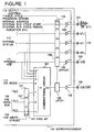
- FIG. 1 there is shown a block diagram of an embodiment of the microprocessor in accordance with the present invention.
- the shown microprocessor includes a group of output terminals 101 for outputting external address signals A 31-0 of 32 bits, an external bus cycle start signal BCYST ⁇ , an external bus cycle period indication signal DS ⁇ indicating that it is in the period of a bus cycle, and others.
- the group of output terminals 101 are represented by a single terminal in Figure 1 for simplification of the drawings.
- the microprocessor 100 also includes another group of output terminals 102 for outputting external bus cycle status signals ST0 to ST2, an output terminal 103 for outputting an external read/write control signal R/ W ⁇ , and another terminal 104 for outputting a space discrimination signal ICE/ USR ⁇ .
- the group of output terminals 101 are connected to outputs of output drivers 105, which have inputs connected to outputs of latches 106, which are in turn coupled to an internal address bus and an internal control bus (both not shown) for receiving internal address signals of 32 bits, an internal bus cycle start signal, an internal bus cycle period indication signal, and others.
- the output drivers 105 and the outputs latches 106 for these signals are represented by a single driver and a single latch, respectively, in Figure 1 for simplification of the drawings.
- the group of output terminals 102 and the output terminal 103 are connected to outputs of further output drivers 105, which have inputs connected to outputs of corresponding latches 106, which are in turn coupled for receiving internal status signals ST0 to ST2 112, and an internal read/write control signal 111.
- the shown microprocessor also includes three latches 107 coupled to receive "bit 2", “bit 1” and “bit 0" of a firmware data bus 108, and controlled by a firmware write strobe signal 109 in such a manner that when the firmware write strobe signal 109 is active, the three bits “bit 2", “bit 1” and “bit 0" of the firmware data bus 108 are latched in the latches 107, respectively.
- the three bits “bit 2", “bit 1” and “bit 0" of the firmware data bus 108 are called a "ERW bit” hereinafter, and the term “firmware” is abbreviated to "F/W” in the specification.
- Outputs of the ERW bit latches 107 are connected to inputs "f", “g” and “h” of a combinational circuit 301, which also receive, at its input “e”, a internal ICE mode signal 110 indicating that the microprocessor 100 itself is put in the ICE mode. Furthermore, the combinational circuit 301 receives, at its inputs "a”, “b”, “c” and “d”, the internal status signals ST2 to ST0 112, and the internal read/write control signal 111.
- An output of the combinational circuit 301 is connected to a still another output latch 106, which has an output connected to a corresponding output driver 105 having an output connected to the ICE/ USR ⁇ output terminal 104.
- All of the output drivers 105 are controlled by an internal output control signal 113, and all of the output latches 106 are controlled by an internal bus cycle progress strobe signal 114, so that all the internal signals supplied to the output latches 106 are latched in the output latches 106 in synchronism to each other.
- the three bits latched in the ERW bit latches 107 are set in such a manner that the "bit 2" corresponds to a bus cycle for an instruction fetch; the "bit 1" corresponds to a bus cycle for a reading other than the instruction fetch; and the "bit 0" corresponds to a bus cycle for a writing.
- an activated bus status of the ERW bits 107, the internal status signals 112 and the internal read/write signal 111 are compared and discriminated in the combinational circuit 301, and if a predetermined condition holds, the combinational circuit 301 outputs an ICE/ USR ⁇ signal 104 of "1".
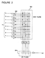
- This combinational circuit 301 can be realized by a programmable logic array as shown in Figure 2, which includes an array of input inverters 302, an AND place 303 programmed as shown, an OR plane 304.
- the combinational circuit 301 In a status in which the "bit 2" and the “bit 0" of the ERW bits 107 are set to “1” and the “bit 1" of the ERW bits 107 is set to "0", namely, when it is set that the instruction fetch bus cycle and the write bus bus cycle are the ICE space access and the read bus cycle other than the instruction fetch is the user space access, the combinational circuit 301 generates the output signal of "1" in response to the internal status signal 112 of (0,1,1) and the read/write signal 111 of "1" as shown at a timing 1 in Figure 3.
- the ICE/ USR ⁇ signal 104 is brought into “1” in synchronism with a rising of a clock just after the output signal of the combinational circuit 301 is brought to "1".
- the ICE/ USR ⁇ signal 104 of "1" indicates that the bus cycle is the ICE space access.
- the combinational circuit 301 generates the output signal of "0" in response to the internal status signal 112 of (0, 0, 0) and the read/write signal 111 of "1” as shown at a timing 2 in Figure 3, so that the ICE/ USR ⁇ signal 104 is brought into “0” in synchronism with a rising of a clock just after the timing 2.
- the combinational circuit 301 generates the output signal of "1” in response to the internal status signal 112 of (0,0,0) and the read/write signal 111 of "0” as shown at a timing 3 in Figure 3, so that the ICE/ USR ⁇ signal 104 is brought into “1” in synchronism with a rising of a clock just after the timing 3.
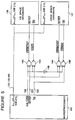
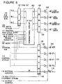
- FIG. 5 there is shown an example of an ICE system incorporating therein the shown microprocessor.
- the external bus cycle start signal BCYST ⁇ 121 and the external bus cycle period indication signal DS ⁇ 122 are respectively supplied through a first pair of AND gates 140 and 142 to the ICE space hardware 126.
- the external bus cycle start signal BCYST ⁇ 121 and the external bus cycle period indication signal DS ⁇ 122 are also respectively supplied through a second pair of AND gates 144 and 146 to the user space hardware 127.
- the first pair of AND gates 140 and 142 is controlled by the ICE/ USR ⁇ signal 104 so that when the ICE/ USR ⁇ signal is of "1" indicating that the access is the ICE space access, the external bus cycle start signal BCYST ⁇ 121 and the external bus cycle period indication signal DS ⁇ 122 are respectively supplied through the first pair of AND gates 140 and 142 to the ICE space hardware 126 as an ICE bus cycle start signal ICEBCYST ⁇ and an ICE bus cycle period indication signal ICEDS ⁇ .
- the second pair of AND gates 144 and 146 is controlled through an inverter 148 by the ICE/ USR ⁇ signal 104 so that if the ICE/ USR ⁇ signal is of "0" indicating that the access is the user space access, the external bus cycle start signal BCYST ⁇ 121 and the external bus cycle period indication signal DS ⁇ 122 are also respectively supplied through the second pair of AND gates 144 and 146 to the user space hardware 127 as a user bus cycle start signal USRBCYST ⁇ and a user bus cycle period indication signal USRDS ⁇ .
- the external bus cycle start signal BCYST ⁇ and the external bus cycle period indication signal DS ⁇ are alternatively supplied to either the ICE space hardware 126 or the user space hardware 127.
- FIG. 6 there is shown a block diagram of an essential part of another embodiment of the microprocessor in accordance with the present invention.
- elements corresponding to those shown in Figure 1 are given the same Reference Numerals, and explanation thereof will be omitted.
- the second embodiment of the microprocessor has an output terminal 130 for the ICE bus cycle start signal ICEBCYST ⁇ , an output terminal 131 for the ICE bus cycle period indication signal ICEDS ⁇ , an output terminal 132 for the user bus cycle start signal USRBCYST ⁇ and an output terminal 130 for the user bus cycle period indication signal USRDS ⁇ .
- the ICE bus cycle start signal ICEBCYST ⁇ 130, the ICE bus cycle period indication signal ICEDS ⁇ 131, the user bus cycle start signal USRBCYST ⁇ 132, and the user bus cycle period indication signal USRDS ⁇ 133 are generated by a combinational circuit 401, which receives the three ERW bits 107, the F/W write strobe signal 109, the internal read/write control signal 111, the internal status signals 112, the internal bus cycle start signal 117 and the internal bus cycle period indication signal 118.
- the combinational circuit 401 can be realized by a programmable logic array as shown in Figure 7, which includes an array of input inverters 402, an AND place 403 programmed as shown, an OR plane 404.
- FIG. 8 there is shown a timing chart illustrating an operation of the microprocessor shown in Figure 6.
- accesses at timings 1, 2 and 4 are the user space access, and the user bus cycle start signal USRBCYST ⁇ 132 and the user bus cycle period indication signal USRDS ⁇ 133 are activated.
- An access at a timing 3 is the ICE space access, and the ICE bus cycle start signal ICEBCYST ⁇ 130 and the ICE bus cycle period indication signal ICEDS ⁇ 131 are activated. Operation other than the above mentioned points are the same as that of the first embodiment.
- the ERW bits 107 are set by the firmware. However, it would be apparent in persons skilled in the art that the ERW bits 107 can be set by software or hardware.
- the microprocessor in accordance with the present invention is characterized in that the discrimination between the use space access and the ICE space access is executed on the basis of the previously set condition and the bus cycle attribute of the read cycle, the write cycle and the instruction fetch cycle.
- This function of the discrimination between the use space access and the ICE space access is realized in the internal circuit of the microprocessor. Therefore, the re-mapping processing in the ICE monitor program becomes unnecessary, and it is possible to avoid the increase of the delay in various control signals.
- all space provided to users as architecture of a microprocessor can be ensured in both of the user space and the ICE space.
Landscapes
- Engineering & Computer Science (AREA)
- Theoretical Computer Science (AREA)
- General Engineering & Computer Science (AREA)
- Physics & Mathematics (AREA)
- General Physics & Mathematics (AREA)
- Computer Hardware Design (AREA)
- Software Systems (AREA)
- Quality & Reliability (AREA)
- Test And Diagnosis Of Digital Computers (AREA)
- Microcomputers (AREA)
- Memory System (AREA)
- Debugging And Monitoring (AREA)
Applications Claiming Priority (2)
| Application Number | Priority Date | Filing Date | Title |
|---|---|---|---|
| JP2128046A JP2611491B2 (ja) | 1990-05-17 | 1990-05-17 | マイクロプロセッサ |
| JP128046/90 | 1990-05-17 |
Publications (3)
| Publication Number | Publication Date |
|---|---|
| EP0463352A2 true EP0463352A2 (fr) | 1992-01-02 |
| EP0463352A3 EP0463352A3 (en) | 1993-07-21 |
| EP0463352B1 EP0463352B1 (fr) | 1999-02-03 |
Family
ID=14975174
Family Applications (1)
| Application Number | Title | Priority Date | Filing Date |
|---|---|---|---|
| EP91108056A Expired - Lifetime EP0463352B1 (fr) | 1990-05-17 | 1991-05-17 | Microprocesseur pour émulateur interne au circuit avec espace d'usager et espace d'émulateur interne au circuit séparé |
Country Status (4)
| Country | Link |
|---|---|
| US (1) | US5396611A (fr) |
| EP (1) | EP0463352B1 (fr) |
| JP (1) | JP2611491B2 (fr) |
| DE (1) | DE69130841T2 (fr) |
Cited By (2)
| Publication number | Priority date | Publication date | Assignee | Title |
|---|---|---|---|---|
| AT405074B (de) * | 1995-07-13 | 1999-05-25 | Rudolf Liberda | Tor, insbesondere schiebetor |
| EP1249759A1 (fr) * | 2001-04-04 | 2002-10-16 | Infineon Technologies AG | Unité commandée par programme |
Families Citing this family (3)
| Publication number | Priority date | Publication date | Assignee | Title |
|---|---|---|---|---|
| JPH081791B2 (ja) * | 1990-08-20 | 1996-01-10 | 三菱電機株式会社 | 投写型陰極線管 |
| US5640542A (en) * | 1993-10-29 | 1997-06-17 | Intel Corporation | On-chip in-circuit-emulator memory mapping and breakpoint register modules |
| CN100498736C (zh) * | 2006-06-26 | 2009-06-10 | 凌阳科技股份有限公司 | 一种仿真器及其与目标板接口的适配方法 |
Family Cites Families (2)
| Publication number | Priority date | Publication date | Assignee | Title |
|---|---|---|---|---|
| US4580213A (en) * | 1982-07-07 | 1986-04-01 | Motorola, Inc. | Microprocessor capable of automatically performing multiple bus cycles |
| US4860246A (en) * | 1985-08-07 | 1989-08-22 | Seiko Epson Corporation | Emulation device for driving a LCD with a CRT display |
-
1990
- 1990-05-17 JP JP2128046A patent/JP2611491B2/ja not_active Expired - Lifetime
-
1991
- 1991-05-17 DE DE69130841T patent/DE69130841T2/de not_active Expired - Fee Related
- 1991-05-17 EP EP91108056A patent/EP0463352B1/fr not_active Expired - Lifetime
-
1994
- 1994-05-31 US US08/251,020 patent/US5396611A/en not_active Expired - Fee Related
Cited By (2)
| Publication number | Priority date | Publication date | Assignee | Title |
|---|---|---|---|---|
| AT405074B (de) * | 1995-07-13 | 1999-05-25 | Rudolf Liberda | Tor, insbesondere schiebetor |
| EP1249759A1 (fr) * | 2001-04-04 | 2002-10-16 | Infineon Technologies AG | Unité commandée par programme |
Also Published As
| Publication number | Publication date |
|---|---|
| DE69130841D1 (de) | 1999-03-18 |
| EP0463352B1 (fr) | 1999-02-03 |
| JP2611491B2 (ja) | 1997-05-21 |
| JPH0423051A (ja) | 1992-01-27 |
| EP0463352A3 (en) | 1993-07-21 |
| DE69130841T2 (de) | 1999-09-16 |
| US5396611A (en) | 1995-03-07 |
Similar Documents
| Publication | Publication Date | Title |
|---|---|---|
| EP0312239B1 (fr) | Dispositif de commande pour un tampon "peps" par message | |
| KR940002755B1 (ko) | 1칩 마이크로 컴퓨터 | |
| US5621883A (en) | Circuit for testing microprocessor memories | |
| EP0312238A2 (fr) | Dispositif de commande pour un tampon "peps" | |
| US5274780A (en) | Bus controller for adjusting a bus master to a bus slave | |
| EP0645776A2 (fr) | Dispositif de mémoire à semi-conducteur mettant en oeuvre un test de mémoire | |
| JP2762138B2 (ja) | メモリコントロールユニット | |
| US5027313A (en) | Apparatus for determining maximum usable memory size | |
| EP0304948B1 (fr) | Processeur de données comprenant une structure de test pour décaleur multiple | |
| EP0757316A1 (fr) | Unité de sélection de dispositifs externes pour processeur de données | |
| EP0408353A2 (fr) | Circuit intégré à semi-conducteur | |
| US5553244A (en) | Reflexively sizing memory bus interface | |
| EP0337463A2 (fr) | Système d'émulation capable de s'adapter aux microordinateurs ayant des capacités différentes de mémoire on-chip | |
| EP0463352A2 (fr) | Microprocesseur pour émulateur interne au circuit avec espace d'usager et espace d'émulateur interne au circuit séparé | |
| US5222226A (en) | Single-chip microprocessor having variable memory address mapping | |
| EP0057096A2 (fr) | Unité de traitement d'information | |
| KR910001708B1 (ko) | 중앙처리장치 | |
| US5126972A (en) | Arrangement and method of ascertaining memory addresses which have been accessed during program execution | |
| EP0334523B1 (fr) | Microprocesseur | |
| US4873628A (en) | Command translating computer | |
| JP2580558B2 (ja) | インタフェース装置 | |
| US4858109A (en) | Program code fetch from data memory arrangement | |
| KR0129918Y1 (ko) | 셀프 테스트 기능을 갖는 메모리장치 | |
| US4841298A (en) | Bit pattern conversion system | |
| JP2970834B2 (ja) | テスト基礎データ生成装置 |
Legal Events
| Date | Code | Title | Description |
|---|---|---|---|
| PUAI | Public reference made under article 153(3) epc to a published international application that has entered the european phase |
Free format text: ORIGINAL CODE: 0009012 |
|
| 17P | Request for examination filed |
Effective date: 19910617 |
|
| AK | Designated contracting states |
Kind code of ref document: A2 Designated state(s): DE FR GB |
|
| PUAL | Search report despatched |
Free format text: ORIGINAL CODE: 0009013 |
|
| AK | Designated contracting states |
Kind code of ref document: A3 Designated state(s): DE FR GB |
|
| 17Q | First examination report despatched |
Effective date: 19970703 |
|
| GRAG | Despatch of communication of intention to grant |
Free format text: ORIGINAL CODE: EPIDOS AGRA |
|
| GRAG | Despatch of communication of intention to grant |
Free format text: ORIGINAL CODE: EPIDOS AGRA |
|
| GRAH | Despatch of communication of intention to grant a patent |
Free format text: ORIGINAL CODE: EPIDOS IGRA |
|
| GRAH | Despatch of communication of intention to grant a patent |
Free format text: ORIGINAL CODE: EPIDOS IGRA |
|
| GRAA | (expected) grant |
Free format text: ORIGINAL CODE: 0009210 |
|
| AK | Designated contracting states |
Kind code of ref document: B1 Designated state(s): DE FR GB |
|
| REF | Corresponds to: |
Ref document number: 69130841 Country of ref document: DE Date of ref document: 19990318 |
|
| ET | Fr: translation filed | ||
| PLBE | No opposition filed within time limit |
Free format text: ORIGINAL CODE: 0009261 |
|
| STAA | Information on the status of an ep patent application or granted ep patent |
Free format text: STATUS: NO OPPOSITION FILED WITHIN TIME LIMIT |
|
| 26N | No opposition filed | ||
| PGFP | Annual fee paid to national office [announced via postgrant information from national office to epo] |
Ref country code: FR Payment date: 20000510 Year of fee payment: 10 |
|
| PGFP | Annual fee paid to national office [announced via postgrant information from national office to epo] |
Ref country code: DE Payment date: 20000515 Year of fee payment: 10 |
|
| PGFP | Annual fee paid to national office [announced via postgrant information from national office to epo] |
Ref country code: GB Payment date: 20000517 Year of fee payment: 10 |
|
| PG25 | Lapsed in a contracting state [announced via postgrant information from national office to epo] |
Ref country code: GB Free format text: LAPSE BECAUSE OF NON-PAYMENT OF DUE FEES Effective date: 20010517 |
|
| GBPC | Gb: european patent ceased through non-payment of renewal fee |
Effective date: 20010517 |
|
| PG25 | Lapsed in a contracting state [announced via postgrant information from national office to epo] |
Ref country code: FR Free format text: LAPSE BECAUSE OF NON-PAYMENT OF DUE FEES Effective date: 20020131 |
|
| PG25 | Lapsed in a contracting state [announced via postgrant information from national office to epo] |
Ref country code: DE Free format text: LAPSE BECAUSE OF NON-PAYMENT OF DUE FEES Effective date: 20020301 |