EP0463580A2 - Nichtflüchtige Halbleiterspeicheranordnung - Google Patents
Nichtflüchtige Halbleiterspeicheranordnung Download PDFInfo
- Publication number
- EP0463580A2 EP0463580A2 EP91110254A EP91110254A EP0463580A2 EP 0463580 A2 EP0463580 A2 EP 0463580A2 EP 91110254 A EP91110254 A EP 91110254A EP 91110254 A EP91110254 A EP 91110254A EP 0463580 A2 EP0463580 A2 EP 0463580A2
- Authority
- EP
- European Patent Office
- Prior art keywords
- memory cells
- memory
- data
- pair
- comprised
- Prior art date
- Legal status (The legal status is an assumption and is not a legal conclusion. Google has not performed a legal analysis and makes no representation as to the accuracy of the status listed.)
- Granted
Links
Images







Classifications
-
- G—PHYSICS
- G11—INFORMATION STORAGE
- G11C—STATIC STORES
- G11C16/00—Erasable programmable read-only memories
- G11C16/02—Erasable programmable read-only memories electrically programmable
- G11C16/06—Auxiliary circuits, e.g. for writing into memory
- G11C16/34—Determination of programming status, e.g. threshold voltage, overprogramming or underprogramming, retention
- G11C16/349—Arrangements for evaluating degradation, retention or wearout, e.g. by counting erase cycles
-
- G—PHYSICS
- G11—INFORMATION STORAGE
- G11C—STATIC STORES
- G11C16/00—Erasable programmable read-only memories
- G11C16/02—Erasable programmable read-only memories electrically programmable
- G11C16/04—Erasable programmable read-only memories electrically programmable using variable threshold transistors, e.g. FAMOS
- G11C16/0408—Erasable programmable read-only memories electrically programmable using variable threshold transistors, e.g. FAMOS comprising cells containing floating gate transistors
- G11C16/0441—Erasable programmable read-only memories electrically programmable using variable threshold transistors, e.g. FAMOS comprising cells containing floating gate transistors comprising cells containing multiple floating gate devices, e.g. separate read-and-write FAMOS transistors with connected floating gates
-
- G—PHYSICS
- G11—INFORMATION STORAGE
- G11C—STATIC STORES
- G11C11/00—Digital stores characterised by the use of particular electric or magnetic storage elements; Storage elements therefor
- G11C11/56—Digital stores characterised by the use of particular electric or magnetic storage elements; Storage elements therefor using storage elements with more than two stable states represented by steps, e.g. of voltage, current, phase, frequency
- G11C11/5621—Digital stores characterised by the use of particular electric or magnetic storage elements; Storage elements therefor using storage elements with more than two stable states represented by steps, e.g. of voltage, current, phase, frequency using charge storage in a floating gate
-
- G—PHYSICS
- G11—INFORMATION STORAGE
- G11C—STATIC STORES
- G11C16/00—Erasable programmable read-only memories
- G11C16/02—Erasable programmable read-only memories electrically programmable
- G11C16/04—Erasable programmable read-only memories electrically programmable using variable threshold transistors, e.g. FAMOS
- G11C16/0408—Erasable programmable read-only memories electrically programmable using variable threshold transistors, e.g. FAMOS comprising cells containing floating gate transistors
-
- G—PHYSICS
- G11—INFORMATION STORAGE
- G11C—STATIC STORES
- G11C16/00—Erasable programmable read-only memories
- G11C16/02—Erasable programmable read-only memories electrically programmable
- G11C16/06—Auxiliary circuits, e.g. for writing into memory
- G11C16/08—Address circuits; Decoders; Word-line control circuits
-
- G—PHYSICS
- G11—INFORMATION STORAGE
- G11C—STATIC STORES
- G11C16/00—Erasable programmable read-only memories
- G11C16/02—Erasable programmable read-only memories electrically programmable
- G11C16/06—Auxiliary circuits, e.g. for writing into memory
- G11C16/26—Sensing or reading circuits; Data output circuits
-
- G—PHYSICS
- G11—INFORMATION STORAGE
- G11C—STATIC STORES
- G11C16/00—Erasable programmable read-only memories
- G11C16/02—Erasable programmable read-only memories electrically programmable
- G11C16/06—Auxiliary circuits, e.g. for writing into memory
- G11C16/34—Determination of programming status, e.g. threshold voltage, overprogramming or underprogramming, retention
- G11C16/349—Arrangements for evaluating degradation, retention or wearout, e.g. by counting erase cycles
- G11C16/3495—Circuits or methods to detect or delay wearout of nonvolatile EPROM or EEPROM memory devices, e.g. by counting numbers of erase or reprogram cycles, by using multiple memory areas serially or cyclically
-
- H—ELECTRICITY
- H10—SEMICONDUCTOR DEVICES; ELECTRIC SOLID-STATE DEVICES NOT OTHERWISE PROVIDED FOR
- H10B—ELECTRONIC MEMORY DEVICES
- H10B41/00—Electrically erasable-and-programmable ROM [EEPROM] devices comprising floating gates
Definitions
- This invention relates to a non-volatile semiconductor memory device.
- the memory cell of FIG. 1 includes two transistors 1 and 2. Namely, one is a floating gate transistor 2 as a non-volatile memory element having the N-type diffused region 91 as the source, the N-type diffused region 92 as the drain, the floating gate electrode 95 as the floating gate, and the gate electrode 97 as the control gate. The other is a select transistor 1 of enhancement type having the N-type diffused region 92 as the source, the N-type diffused region 93 as the drain, and the gate electrode 99 as the gate. These transistors 1 and 2 are connected in series. As indicated by the equivalent circuit of FIG. 2, the drain and the gate of the transistor 1 are used as the data line DL and the word line WL, respectively.
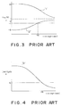
- the threshold voltage of the floating gate transistor takes a substantially negative value, e.g., -5 volts. For this reason, a current flows even if the potential on the control gate is zero volts.
- the potential on the control gate is set to zero volts.
- the judgment as to whether the data stored in the memory cell is "0" or "1" is carried out by setting the operating point of the sense amplifier circuit, i.e., sense potential so that a suitable current flows in the memory cell. This sense potential is set to about -1 volt as indicated by the single dotted lines.
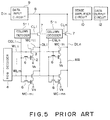
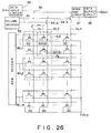
- Respective column lines DLl to DLn are connected in common to a bus line 8 through column select transistors 7.
- the gates of the transistors 7 are connected to the corresponding column decoders 5 through column select lines CLl to CLn, respectively.
- a data input circuit 9 and a sense amplifier circuit 10 are connected to the bus line 8.
- the data input circuit 9 outputs data of "0" or “1” level depending on a write data signal Din inputted from the external.
- the sense amplifier circuit 10 detects, as “0” or "1", the level of data stored in a selected memory cell MC.
- the sense amplifier circuit 10 applies a bias voltage necessary for the readout of data to a corresponding data line DL.
- the sense amplifier circuit 10 includes a bias circuit.
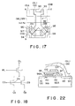
- a non-volatile semiconductor memory device comprising: a plurality of floating gate transistors constituting non-volatile memory cells and forming a cell array or arrays substantially in a matrix form comprised of said memory cells, a plurality of data lines for transmitting data to the memory cells of respective columns of said cell array or arrays and receiving data therefrom, word lines for selecting the memory cells of respective rows of said cell array or arrays to connect selected memory cells to corresponding data lines, respectively, a column decoder for selecting said data lines, and a row decoder for selecting said word lines, a pair of memory cells of said plurality of memory cells selected by said respective word lines being connected to said respective data lines by the common junction where drains of said pair of memory cells are commonly connected, select transistors turned ON and OFF by said word lines being provided between said common junction and the drains of said respective pair of memory cells, each one bit data memory unit being comprised of said two non-volatile memory cells and one of said select transistors.
- select transistor may be provided for every memory cell, but only one select transistor may be provided in common to two transistors.
- An employment of the arrangement including one select transistor is advantageous for miniaturization.
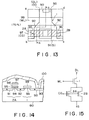
- FIGS. 6 and 7 there is shown a portion of EEPROM (a unit cell, 1 bit data memory unit) devised by the inventor of this invention, constructed so that respective memory cells can be miniaturized to more degree.
- FIG. 6 showing a plane view of an actual arrangement, the section encompassed by single-dotted lines a, b, c and d represents a unit memory cell.
- FIG. 7 is a cross sectional view taken along the A-A line of FIG. 6.
- the configuration shown in FIG. 7 differs from the configuration shown in FIG. 1 in that the insulating oxide film 94 of the floating gate transistor 2 is formed as a thin film of 100 angstroms, and that the thin film portion 94A of FIG. 1 for allowing a tunnel current to flow therein is omitted.
- the same reference numerals are attached to parts similar to those in FIG. 1, respectively.
- the size in a thickness direction of the floating gate transistor 2 can be reduced to a large degree.
- the size in a lateral direction is determined, as seen from FIG. 6, by the contact portion 90. Namely, by the size l1 of the contact 90, the margin l2 between the contact 90 and the drain n+ diffused layer 93, and the size l3 of the field isolation portion between adjacent drain n+ diffused layer 93, the size of the cell is determined.
- These sizes are fixed in the manufacturing process determined in advance. For this reason, it is difficult in practice to arbitrarily reduce these respective sizes. In view of this, even when an attempt is made to use two (a pair of) memory cells of FIGS. 6 and 7 to construct the abovementioned high reliability non-volatile semiconductor memory (1 bit data memory unit), the chip size becomes large also in this case. Accordingly, it is considered difficult to realize a large capacity memory device.
- FIG. 6 differs from that of FIG. 6 in that a single contact is formed in common to two (a pair of) cells of the NAND structure of the cell including transistors 1A and 2A and the cell including transistors 1B and 2B. Its equivalent circuit is shown in FIG. 10.
- a single contact 90 When provision of a single contact 90 is employed, the size in a lateral direction of the memory cell is not determined by the contact portion 90, but is determined by the width W1 of the floating gate 95 and the distance W2 between the floating gates 95 and 95.
- the operational mode is the "1" write mode
- the potential V DL on the data line DL is caused to have zero volts (data input "1").
- the floating gate FG has substantially no potential difference between the floating gate FG and the control gate CG, resulting in substantially zero volts. In this case, there is no movement of electrons.
- This operation is called a data "1" write operation.
- While such a memory cell is suitable for miniaturization, it is required to simultaneously erase a plurality of memory cells (all memory cells in the chip according to the circumstances) at the time of erase operation to make a control such that its threshold value is equal to a fixed value.
- a tunnel current flows in the oxide film at the time of erase operation, there might take place unsatisfactory operation such that electrons are trapped by defect, etc. in the oxide film, so the erasing characteristic is deteriorated by repetition of writing and/or erasing (W/E).
- W/E writing and/or erasing
- such an unsatisfactory operation may take place at a certain probability in an eventual manner.
- At the initial stage where, e.g., about 10,000 times of W/E are carried out, about 1 to several bits may be unsatisfactorily erased in the case of 1 M bit memory.
Landscapes
- Engineering & Computer Science (AREA)
- Microelectronics & Electronic Packaging (AREA)
- Computer Hardware Design (AREA)
- Non-Volatile Memory (AREA)
- Semiconductor Memories (AREA)
- Read Only Memory (AREA)
Applications Claiming Priority (2)
| Application Number | Priority Date | Filing Date | Title |
|---|---|---|---|
| JP164678/90 | 1990-06-22 | ||
| JP16467890A JP2685966B2 (ja) | 1990-06-22 | 1990-06-22 | 不揮発性半導体記憶装置 |
Publications (3)
| Publication Number | Publication Date |
|---|---|
| EP0463580A2 true EP0463580A2 (de) | 1992-01-02 |
| EP0463580A3 EP0463580A3 (en) | 1993-06-09 |
| EP0463580B1 EP0463580B1 (de) | 1999-03-17 |
Family
ID=15797767
Family Applications (1)
| Application Number | Title | Priority Date | Filing Date |
|---|---|---|---|
| EP91110254A Expired - Lifetime EP0463580B1 (de) | 1990-06-22 | 1991-06-21 | Nichtflüchtige Halbleiterspeicheranordnung |
Country Status (5)
| Country | Link |
|---|---|
| US (1) | US5592001A (de) |
| EP (1) | EP0463580B1 (de) |
| JP (1) | JP2685966B2 (de) |
| KR (1) | KR950010725B1 (de) |
| DE (1) | DE69130993T2 (de) |
Cited By (3)
| Publication number | Priority date | Publication date | Assignee | Title |
|---|---|---|---|---|
| CN1039172C (zh) * | 1994-01-19 | 1998-07-15 | 爱特梅尔股份有限公司 | 减小非易失性存储单元中的应力 |
| EP0903748A3 (de) * | 1997-09-18 | 2000-11-15 | SANYO ELECTRIC Co., Ltd. | Nichtflüchtige Halbleiterspeicheranordnung |
| EP0903749A3 (de) * | 1997-09-18 | 2000-11-15 | SANYO ELECTRIC Co., Ltd. | Nichtflüchtige Halbleiterspeicheranordnung |
Families Citing this family (32)
| Publication number | Priority date | Publication date | Assignee | Title |
|---|---|---|---|---|
| JP2596695B2 (ja) * | 1993-05-07 | 1997-04-02 | インターナショナル・ビジネス・マシーンズ・コーポレイション | Eeprom |
| JP3469362B2 (ja) * | 1994-08-31 | 2003-11-25 | 株式会社東芝 | 半導体記憶装置 |
| JP2980012B2 (ja) * | 1995-10-16 | 1999-11-22 | 日本電気株式会社 | 不揮発性半導体記憶装置 |
| US5966601A (en) * | 1997-01-21 | 1999-10-12 | Holtek Microelectronics Inc. | Method of making non-volatile semiconductor memory arrays |
| JPH1187658A (ja) * | 1997-09-05 | 1999-03-30 | Mitsubishi Electric Corp | メモリセルおよびそれを備える不揮発性半導体記憶装置 |
| US6157574A (en) * | 1998-04-01 | 2000-12-05 | National Semiconductor Corporation | Erasable frohmann-bentchkowsky memory transistor that stores multiple bits of data |
| US6118691A (en) * | 1998-04-01 | 2000-09-12 | National Semiconductor Corporation | Memory cell with a Frohmann-Bentchkowsky EPROM memory transistor that reduces the voltage across an unprogrammed memory transistor during a read |
| US6055185A (en) * | 1998-04-01 | 2000-04-25 | National Semiconductor Corporation | Single-poly EPROM cell with CMOS compatible programming voltages |
| US6141246A (en) * | 1998-04-01 | 2000-10-31 | National Semiconductor Corporation | Memory device with sense amplifier that sets the voltage drop across the cells of the device |
| US6081451A (en) * | 1998-04-01 | 2000-06-27 | National Semiconductor Corporation | Memory device that utilizes single-poly EPROM cells with CMOS compatible programming voltages |
| JP3999900B2 (ja) * | 1998-09-10 | 2007-10-31 | 株式会社東芝 | 不揮発性半導体メモリ |
| TW445649B (en) * | 1999-06-09 | 2001-07-11 | Sanyo Electric Co | Semiconductor memory and method for operating a semiconductor memory |
| DE19946883A1 (de) * | 1999-09-30 | 2001-04-12 | Micronas Gmbh | Verfahren zur Herstellung eines integrierten CMOS-Halbleiterspeichers |
| JP4484344B2 (ja) * | 2000-09-08 | 2010-06-16 | ローム株式会社 | 不揮発性半導体記憶装置 |
| EP1227496A1 (de) * | 2001-01-17 | 2002-07-31 | Cavendish Kinetics Limited | Nichtflüchtiger speicher |
| JP4256222B2 (ja) * | 2003-08-28 | 2009-04-22 | 株式会社東芝 | 不揮発性半導体記憶装置 |
| JP2006048749A (ja) * | 2004-07-30 | 2006-02-16 | Seiko Epson Corp | 不揮発性記憶装置及び不揮発性記憶装置のデータ書き込み方法 |
| JP2007141286A (ja) * | 2005-11-15 | 2007-06-07 | Nec Electronics Corp | 半導体集積回路装置及びその制御方法 |
| JP2007266377A (ja) * | 2006-03-29 | 2007-10-11 | Fujitsu Ltd | 半導体装置 |
| US7626868B1 (en) * | 2007-05-04 | 2009-12-01 | Flashsilicon, Incorporation | Level verification and adjustment for multi-level cell (MLC) non-volatile memory (NVM) |
| JP5629968B2 (ja) * | 2008-09-19 | 2014-11-26 | 凸版印刷株式会社 | 不揮発性半導体メモリセル及び不揮発性半導体メモリ装置 |
| JP5417853B2 (ja) * | 2009-01-15 | 2014-02-19 | 凸版印刷株式会社 | 不揮発性半導体メモリセル及び不揮発性半導体メモリ装置 |
| JP5572953B2 (ja) * | 2009-01-15 | 2014-08-20 | 凸版印刷株式会社 | 不揮発性半導体メモリセル及び不揮発性半導体メモリ装置 |
| JP5347649B2 (ja) * | 2009-03-30 | 2013-11-20 | 凸版印刷株式会社 | 不揮発性半導体メモリ装置 |
| JP2010231872A (ja) * | 2009-03-30 | 2010-10-14 | Toppan Printing Co Ltd | 不揮発性半導体メモリ装置 |
| JP5522296B2 (ja) * | 2013-06-03 | 2014-06-18 | 凸版印刷株式会社 | 不揮発性半導体記憶装置 |
| US10892266B2 (en) | 2016-01-19 | 2021-01-12 | Ememory Technology Inc. | Nonvolatile memory structure and array |
| US9847133B2 (en) | 2016-01-19 | 2017-12-19 | Ememory Technology Inc. | Memory array capable of performing byte erase operation |
| US10924112B2 (en) * | 2019-04-11 | 2021-02-16 | Ememory Technology Inc. | Bandgap reference circuit |
| CN112086115B (zh) * | 2019-06-14 | 2023-03-28 | 力旺电子股份有限公司 | 存储器系统 |
| US10984878B1 (en) * | 2020-02-11 | 2021-04-20 | Taiwan Semiconductor Manufacturing Company, Ltd | One-time programmable memory bit cell |
| KR20240132861A (ko) * | 2023-02-27 | 2024-09-04 | 에스케이하이닉스 주식회사 | 반도체 메모리 장치 |
Family Cites Families (8)
| Publication number | Priority date | Publication date | Assignee | Title |
|---|---|---|---|---|
| JPS6046554B2 (ja) * | 1978-12-14 | 1985-10-16 | 株式会社東芝 | 半導体記憶素子及び記憶回路 |
| JPH0715973B2 (ja) * | 1984-11-29 | 1995-02-22 | 新技術事業団 | 半導体不揮発性メモリ |
| JP2607504B2 (ja) * | 1987-02-20 | 1997-05-07 | 株式会社東芝 | 不揮発性半導体メモリ |
| IT1215380B (it) * | 1987-03-12 | 1990-02-08 | Sgs Microelettronica Spa | Cella di memoria eprom a due semicelle simmetriche con gate flottante separata. |
| IT1214246B (it) * | 1987-05-27 | 1990-01-10 | Sgs Microelettronica Spa | Dispositivo di memoria non volatile ad elevato numero di cicli di modifica. |
| JP2664685B2 (ja) * | 1987-07-31 | 1997-10-15 | 株式会社東芝 | 半導体装置の製造方法 |
| JPH01196794A (ja) * | 1988-01-30 | 1989-08-08 | Toshiba Corp | 不揮発性半導体記憶装置 |
| FR2635410B1 (fr) * | 1988-08-11 | 1991-08-02 | Sgs Thomson Microelectronics | Memoire de type eprom a haute densite d'integration avec une organisation en damier et un facteur de couplage ameliore et procede de fabrication |
-
1990
- 1990-06-22 JP JP16467890A patent/JP2685966B2/ja not_active Expired - Fee Related
-
1991
- 1991-06-21 DE DE69130993T patent/DE69130993T2/de not_active Expired - Fee Related
- 1991-06-21 EP EP91110254A patent/EP0463580B1/de not_active Expired - Lifetime
- 1991-06-22 KR KR1019910010387A patent/KR950010725B1/ko not_active Expired - Fee Related
-
1996
- 1996-04-05 US US08/626,148 patent/US5592001A/en not_active Expired - Fee Related
Cited By (3)
| Publication number | Priority date | Publication date | Assignee | Title |
|---|---|---|---|---|
| CN1039172C (zh) * | 1994-01-19 | 1998-07-15 | 爱特梅尔股份有限公司 | 减小非易失性存储单元中的应力 |
| EP0903748A3 (de) * | 1997-09-18 | 2000-11-15 | SANYO ELECTRIC Co., Ltd. | Nichtflüchtige Halbleiterspeicheranordnung |
| EP0903749A3 (de) * | 1997-09-18 | 2000-11-15 | SANYO ELECTRIC Co., Ltd. | Nichtflüchtige Halbleiterspeicheranordnung |
Also Published As
| Publication number | Publication date |
|---|---|
| US5592001A (en) | 1997-01-07 |
| KR950010725B1 (ko) | 1995-09-22 |
| JPH0457293A (ja) | 1992-02-25 |
| EP0463580A3 (en) | 1993-06-09 |
| KR920001720A (ko) | 1992-01-30 |
| JP2685966B2 (ja) | 1997-12-08 |
| DE69130993D1 (de) | 1999-04-22 |
| EP0463580B1 (de) | 1999-03-17 |
| DE69130993T2 (de) | 1999-07-29 |
Similar Documents
| Publication | Publication Date | Title |
|---|---|---|
| US5592001A (en) | Non-volatile semiconductor memory device | |
| KR0145475B1 (ko) | 낸드구조를 가지는 불휘발성 반도체 메모리의 프로그램장치 및 방법 | |
| KR100206709B1 (ko) | 멀티비트 불휘발성 반도체 메모리의 셀 어레이의 구조 및 그의 구동방법 | |
| KR100187196B1 (ko) | 불휘발성 반도체 메모리 장치 | |
| US7505327B2 (en) | Method of controlling a semiconductor device by a comparison of times for discharge of bit lines connected to different memory cell arrays | |
| JP4966472B2 (ja) | 小ページサイズの書込みと消去を有する電気的消去可能プログラマブル読出し専用メモリ | |
| US7151693B2 (en) | Method of writing data to a non-volatile semiconductor memory | |
| EP0639860B1 (de) | Nichtflüchtiger Halbleiterspeicher | |
| US5740107A (en) | Nonvolatile integrated circuit memories having separate read/write paths | |
| US6570810B2 (en) | Contactless flash memory with buried diffusion bit/virtual ground lines | |
| US6407941B1 (en) | Segmented non-volatile memory array with multiple sources having improved source line decode circuitry | |
| US20030201467A1 (en) | Method of forming memory arrays based on a triple-polysilicon source-side injection non-volatile memory cell | |
| US10446245B2 (en) | Non-volatile memory array with memory gate line and source line scrambling | |
| KR960016106B1 (ko) | 비 휘발성 반도체 메모리 장치 | |
| JPH03283200A (ja) | 不揮発性半導体記憶装置及びこれに用いられるメモリセルトランジスタのしきい値電圧の測定方法 | |
| KR0172422B1 (ko) | 스냅백 브레이크다운 현상을 제거한 공통 소오스 라인 제어회로 | |
| US20080191266A1 (en) | Highly reliable NAND flash memory using a five side enclosed floating gate storage elements | |
| US4402064A (en) | Nonvolatile memory | |
| EP0387889B1 (de) | Nichtflüchtiger Halbleiterspeicher | |
| US7405972B1 (en) | Non-volatile memory array | |
| US5303184A (en) | Non-volatile semiconductor memory having commonly used source or drain regions of floating gate type transistors | |
| JP2647101B2 (ja) | 不揮発性半導体メモリ装置 | |
| JP3023330B2 (ja) | 不揮発性半導体記憶装置 | |
| US6005805A (en) | Nonvolatile semiconductor device with a verify function | |
| JPH07120716B2 (ja) | 半導体記憶装置 |
Legal Events
| Date | Code | Title | Description |
|---|---|---|---|
| PUAI | Public reference made under article 153(3) epc to a published international application that has entered the european phase |
Free format text: ORIGINAL CODE: 0009012 |
|
| 17P | Request for examination filed |
Effective date: 19910621 |
|
| AK | Designated contracting states |
Kind code of ref document: A2 Designated state(s): DE FR GB |
|
| PUAL | Search report despatched |
Free format text: ORIGINAL CODE: 0009013 |
|
| AK | Designated contracting states |
Kind code of ref document: A3 Designated state(s): DE FR GB |
|
| 17Q | First examination report despatched |
Effective date: 19960102 |
|
| GRAG | Despatch of communication of intention to grant |
Free format text: ORIGINAL CODE: EPIDOS AGRA |
|
| GRAG | Despatch of communication of intention to grant |
Free format text: ORIGINAL CODE: EPIDOS AGRA |
|
| GRAH | Despatch of communication of intention to grant a patent |
Free format text: ORIGINAL CODE: EPIDOS IGRA |
|
| GRAH | Despatch of communication of intention to grant a patent |
Free format text: ORIGINAL CODE: EPIDOS IGRA |
|
| GRAA | (expected) grant |
Free format text: ORIGINAL CODE: 0009210 |
|
| AK | Designated contracting states |
Kind code of ref document: B1 Designated state(s): DE FR GB |
|
| PG25 | Lapsed in a contracting state [announced via postgrant information from national office to epo] |
Ref country code: FR Free format text: LAPSE BECAUSE OF FAILURE TO SUBMIT A TRANSLATION OF THE DESCRIPTION OR TO PAY THE FEE WITHIN THE PRESCRIBED TIME-LIMIT Effective date: 19990317 |
|
| REF | Corresponds to: |
Ref document number: 69130993 Country of ref document: DE Date of ref document: 19990422 |
|
| PGFP | Annual fee paid to national office [announced via postgrant information from national office to epo] |
Ref country code: FR Payment date: 19990610 Year of fee payment: 9 |
|
| EN | Fr: translation not filed | ||
| PLBE | No opposition filed within time limit |
Free format text: ORIGINAL CODE: 0009261 |
|
| STAA | Information on the status of an ep patent application or granted ep patent |
Free format text: STATUS: NO OPPOSITION FILED WITHIN TIME LIMIT |
|
| 26N | No opposition filed | ||
| REG | Reference to a national code |
Ref country code: GB Ref legal event code: IF02 |
|
| PGFP | Annual fee paid to national office [announced via postgrant information from national office to epo] |
Ref country code: GB Payment date: 20050615 Year of fee payment: 15 |
|
| PGFP | Annual fee paid to national office [announced via postgrant information from national office to epo] |
Ref country code: DE Payment date: 20060615 Year of fee payment: 16 |
|
| PG25 | Lapsed in a contracting state [announced via postgrant information from national office to epo] |
Ref country code: GB Free format text: LAPSE BECAUSE OF NON-PAYMENT OF DUE FEES Effective date: 20060621 |
|
| GBPC | Gb: european patent ceased through non-payment of renewal fee |
Effective date: 20060621 |
|
| PG25 | Lapsed in a contracting state [announced via postgrant information from national office to epo] |
Ref country code: DE Free format text: LAPSE BECAUSE OF NON-PAYMENT OF DUE FEES Effective date: 20080101 |