EP0464145B1 - Elektronische kondensatorwasserwaage mit selbsttätiger elektrodenauswahl - Google Patents
Elektronische kondensatorwasserwaage mit selbsttätiger elektrodenauswahl Download PDFInfo
- Publication number
- EP0464145B1 EP0464145B1 EP90905895A EP90905895A EP0464145B1 EP 0464145 B1 EP0464145 B1 EP 0464145B1 EP 90905895 A EP90905895 A EP 90905895A EP 90905895 A EP90905895 A EP 90905895A EP 0464145 B1 EP0464145 B1 EP 0464145B1
- Authority
- EP
- European Patent Office
- Prior art keywords
- electrode
- electrodes
- sensor
- determining
- capacitance
- Prior art date
- Legal status (The legal status is an assumption and is not a legal conclusion. Google has not performed a legal analysis and makes no representation as to the accuracy of the status listed.)
- Expired - Lifetime
Links
Images








Classifications
-
- G—PHYSICS
- G01—MEASURING; TESTING
- G01C—MEASURING DISTANCES, LEVELS OR BEARINGS; SURVEYING; NAVIGATION; GYROSCOPIC INSTRUMENTS; PHOTOGRAMMETRY OR VIDEOGRAMMETRY
- G01C9/00—Measuring inclination, e.g. by clinometers, by levels
- G01C9/18—Measuring inclination, e.g. by clinometers, by levels by using liquids
- G01C9/20—Measuring inclination, e.g. by clinometers, by levels by using liquids the indication being based on the inclination of the surface of a liquid relative to its container
-
- G—PHYSICS
- G01—MEASURING; TESTING
- G01C—MEASURING DISTANCES, LEVELS OR BEARINGS; SURVEYING; NAVIGATION; GYROSCOPIC INSTRUMENTS; PHOTOGRAMMETRY OR VIDEOGRAMMETRY
- G01C9/00—Measuring inclination, e.g. by clinometers, by levels
- G01C9/02—Details
- G01C9/06—Electric or photoelectric indication or reading means
Definitions
- the invention relates to an inclination measuring method and device for measurement of angles relative to a horizontal plane.
- the invention in particular relates to a sensing method and device using electrical capacitance to measure angles.
- GB 2 204 136 is directed to an inclination sensor for measuring angles and flatness and includes a differential capacitor with a coupled evaluation device.
- the differential capacitor is disposed in a closed chamber and formed from a pair of identical capacitor plates, an electrically conductive fluid, a conductor as a counter electrode and a dielectric of a solid insulating layer applied to the plates. No particular circuit or method for processing the resulting signal is disclosed.
- EP 0 196 735 is directed to a differential capacitance detector having two sensor capacitors, each driving an associated one-shot multivibrator.
- the pulse width of the multivibrator output is representative of the capacity of the associated sensor capacitor.
- the comparator then compares these two pulse widths and provides an output signal including both the sign and the amplitude of the difference as an indication of the degree of inclination.
- a number of known inclination measurement devices utilize a fluid or fluids in a chamber with two or more electrodes that are partially covered by the fluid(s), with the covered electrode areas being dependent upon the angle of inclination.
- Such devices are typically a conductive type or capacitive type.
- the fluid In a conductive type device, the fluid has a specific conductivity, and as the contact area between the fluid and a pair of electrodes varies, the resistance between the two electrodes varies. The fluid in this case must electrically contact both electrodes for proper operation and the conductivity of the fluid must be carefully controlled for repeatable performance.
- a capacitive type of device 1 see Figure 1
- a highly dielectric (i.e. non-conductive) type fluid 2 is used.
- the fluid-covered i.e.
- a capacitive inclination sensor device (20) comprising:
- the present invention overcomes the prior art deficiencies by utilizing, in one embodiment, a thin film of insulating material over a coplanar electrode pair to form a capacitive dielectric, and by using a conductive fluid electrically contacting a third, common electrode, with the fluid forming a common capacitive electrode.
- the two capacitors formed by this configuration thus have a differential capacitance that is linear with the angle of inclination, the angle being related to the relative areas of the two electrodes which the conductive fluid covers (i.e. the relative wetted areas of the two electrodes).
- the capacitive sensor in accordance with this invention differs from a prior art variable dielectric capacitor in that the fluid introduced between the plates is electrically conductive, with one of the two plates of any given capacitive element insulated from the fluid by a dielectric layer.
- the fluid thus serves as a conductive liquid capacitor "plate", which is a unique feature of the invention.
- a capacitive type inclinometer sensor in one embodiment of the invention includes at least two coplanar sensor electrodes formed on one end wall of a cylindrical cavity with at least one common electrode (for electrically contacting the conductive fluid) formed on the other end wall of the cavity or alternatively on the interior circular wall of the cavity.
- the cavity is partially filled with a conductive fluid with the remainder of the volume containing air.
- the sensor electrodes are dielectrically isolated from the conductive fluid by the dielectric insulating film, with the common electrode electrically contacting the conductive fluid.
- the sensor electrodes consist of four quadrant-shaped conductive plates of equal area with a gap between them. When the fluid equally covers two of the sensor electrodes, two equal value capacitors are formed.
- the sensor electrodes are two semicircular plates, both with equal areas.
- the sensor electrodes provide an indication that the sensor is level (two equal value capacitors) or not level (unequal value capacitors).
- a similar sensor electrode assembly, rotated 90° relative to the plane of the first sensor indicates plumb or not plumb, so that the two sensors together, fixed to a frame, make up a familiar carpenter's level type of device.
- either the two or four sensor electrode versions can be used to indicate any measure of inclination in degrees.
- the present invention also includes a one sensor electrode embodiment, whereby absolute, not differential, capacitance is measured.
- conventional indicating means such as for example, a bell, tone, light, or digital readout
- indicating means such as for example, a bell, tone, light, or digital readout
- Utilizing a null condition of two differential signals from two sensor electrodes to indicate a level condition eliminates error sources which equally affect the two signals. That is, any common mode error source is eliminated.
- the invention uniquely uses an insulated capacitive sensor with a conductive fluid, the fluid conductivity has little effect on the sensor operation. This is due to the insulation resistance of the capacitive bridge dielectric insulating film being magnitudes larger than the fluid conductivity. The dominant factor is then the capacitive insulation resistance.
- Figure 1 shows a prior art capacitive sensor.
- Figure 2A is an exploded view of one embodiment of the invention.
- Figure 2B is a cross section view of the sensor assembly shown in Figure 2A through line B-B in Figure 2A.
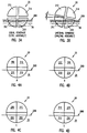
- Figures 3A and 3B show the operation of one embodiment of the operation.
- Figures 4A to 4D show four positions of the embodiment of Figures 3A and 3B.
- Figure 5 is a simplified electrical schematic of the sensor assembly electronics interface of one embodiment of the invention.
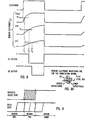
- Figure 6 shows waveforms associated with the circuit of Figure 5.
- Figure 7 is a more detailed electrical schematic of the embodiment of Figure 5.
- Figure 8 shows electrical wave forms associated with the circuit of Figure 7.
- Figure 9 shows the dithering window waveforms associated with the circuit of Figure 7.
- Figures 10A-10H depict eight rotational positions and the electrode pair relationships for each position of the sensor assembly in another embodiment of the invention.
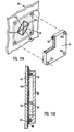
- Figure 11A shows an exploded view of a sensor assembly.
- Figure 11B shows a cross section of the sensor assembly of Figure 11A.
- Figure 12A shows a substrate of another sensor assembly.
- Figures 12B, 12C show cross sections of the sensor assembly of Figure 12A.
- Figure 13 shows a simplified schematic of one embodiment of the invention.
- Figure 14 shows waveforms associated with Figure 13.
- Figure 15 shows a more detailed schematic of the embodiment of Figure 13.
- Figures 16A, 16B, 17 show waveforms associated with the embodiment of Figure 15.
- Figure 18 shows diagrammatically how the electrode autoselect operates.
- Figure 19A shows a block diagram of a level device.
- Figure 19B shows the power switch of Figure 19A.
- Figure 20 shows a schematic for the device of Figure 19A.
- the basic sensor assembly 20 (see exploded view Figure 2A) consists of four identical co-planar sensor electrode plates 21A, 21B, 21C, 21D arranged in quadrants.
- the sensor plates 21A, 21B, 21C, 21D are covered with a thin dielectric film 22 (see Figure 2B for an assembled cross sectional view of assembly 20 through line B-B of Figure 2A) and form an end wall of a cavity 24 that partially contains a conductive fluid 26.
- the main body of the cavity 24, that is the remaining end wall 28A and the cylinder wall 28B, are formed by a metal cup 28 which electrically contacts the conductive fluid 26, acting as a common electrode, as well as completing a sealed container for the fluid 26.
- Sensor plates 21A, 21B, 21C, 21D are conventionally formed by etching a copper layer deposited on a piece of laminated printed circuit board 32.
- the level of fluid 26 is shown at 26B.
- sensor electrodes 21A, 21D are shown slightly separated from printed circuit board 32. In one embodiment, there is no such separation.
- dielectric film 22 is in direct contact with sensor electrodes 21A, 21D, with no separation between dielectric film 22 and sensor electrodes 21A, 21D.
- Conductive fluid 26 is a mixture of alcohol and water, with 1% to 30% water and the rest alcohol. The proportion of water is 1% in one embodiment. Cavity 24 is 45% filled with fluid 26. The rest of cavity 24 is filled with air although an inert gas such as nitrogen can also be used.
- Gap “h” (see Figure 2A) between sensor plates such as 21A and 21B is, in one embodiment, about 0.020 inches (0.5 mm). Sensor electrodes 21A, 21B, 21C, 21D have a combined diameter of about 0.25" to 2" (0.6 cm to 5 cm) in this embodiment. Gap “V” (see Figure 2B) between sensor electrodes 21A, 21B, 21C, 21D and common electrode metal cup 28 is, in one embodiment, about 0.150" (3.8 mm). Naturally the dimensions of the sensor electrodes 21A, 21B, 21C, 21D and of the gaps “h” and “V” can vary as desired and appropriate.
- Metal cap 28 is fastened to printed circuit board 32 by means of conventional fasteners (such as rivets, not shown) which pass through the holes 34A, 34B, etc. in cylinder wall 28B of metal cap 28 and into corresponding holes 36A, 36B, etc. in printed circuit board 32.
- conventional fasteners such as rivets, not shown
- Alternate embodiments of the sensor electrodes 21A, 21B, 21C, 21D include forming them by conductive ink printed on an insulating substrate, or using conventional flex circuits (flexible insulating material on which is formed conductors) for the sensor electrodes 21A, 21B, 21C, 21D.
- Dielectric film layer 22 is preferably a layer about .0005" to .005" (.013 mm to .13 mm) thick of conventional solder mask material, formed over electrodes 21A, 21B, 21C, 21D.
- Other insulators such as Mylar or a similar flexible polyester sheet
- Kapton or a similar flexible polyamide sheet is a suitable dielectric layer.
- Electrodes 21A, 21B, 21C, 21D are, in one embodiment of the invention, quadrant shaped as shown in Figure 2A.
- electrodes 21A, 21B, 21C, 21D are triangular in shape, i.e., instead of being a 90° section of a circle, each sensor electrode is, for example, a 30° section of a circle.
- the electrode shape is not a critical feature of the invention.
- the electronics circuitry provided in one embodiment of the invention then senses this balanced or unbalanced differential capacitance and suitably indicates the state to the user.
- the sensor assembly 20 is utilized to indicate a level condition in any one of four different positions, shown in Figures 4A to 4D with the sensor electrodes 21A, 21B, 21C, 21D.
- the gaps between sensor electrodes 21A, 21B, 21C, 21D are not shown in Figures 4A to 4D for simplicity.
- No pair of diagonal electrodes such as 21A and 21C or 21B and 21D are 'active' at the same time, where the electrode pair partially covered by the fluid 26 is considered to be active; for example, electrodes 21B and 21C are active in Figure 4A.
- the diagonal electrode pair 21A and 21C, 21C is active and 21A is not.
- 21B is active and 21D is not.
- the electronics circuitry in accordance with the invention uses the charge time of an R-C circuit, with the C (capacitance) being formed chiefly by the sensor electrode capacitances. By comparing the charge times of the various sensor electrodes, the position of the assembly can be determined.
- Figure 5 shows a simplified circuit diagram of the sensor electronics circuitry for purposes of illustration.
- V E The provided excitation voltage, V E , (preferably a conventional square wave) charges the sensor electrode capacitors EC1 and EC2 through resistors R1 and R2 when the voltage is high.
- EC1 for example is the capacitor formed by sensor electrode 21B and common electrode 28;
- EC2 for example is the capacitor formed by sensor electrode 21C and common electrode 28, of Figure 3A.
- Both electrode capacitors EC1, EC2 are quickly discharged by diodes D1 and D2 when the excitor voltage, V E , goes from high to low. Voltage V E is low for a longer time than it is high (see Figure 6) to ensure that the capacitors EC1, EC2 are fully discharged before starting a new cycle.
- the diodes D1, D2 provide almost all of the discharge in a very short period of time with the resistors R1,R2 providing a more long term complete discharge after the diodes D1,D2 are no longer in forward conduction (i.e., when the capacitor EC1, EC2 voltages decrease below about 0.5 volts).
- FIG. 6 shows waveforms representing voltages vs. time at points V E , V1, V2, V3, and V4 as shown in Figure 5.
- excitor voltage V E is shown as a series of periodic voltage pulses, with each pulse being shorter in duration than the time between pulses.
- Voltages V1, V2 (the input signals to respectively Schmitt triggers U1, U2) thus are shown as rising and falling with with V E .
- Voltages V3 and V4 (the output signals of respectively Schmitt triggers U1,U2), are shown as falling at a time difference delta, which indicates the out of level condition.
- the Schmitt triggers U1, U2 are dual input NAND gate types, with each of the two NAND input terminals being a Schmitt trigger input terminal.
- a NAND (or NOT AND) gate conventionally logically functions according to the following truth table: Input Output A B 0 0 1 0 1 1 1 0 1 1 1 0 That is, both input signals must be a '1' before the output signal will go to '0'.
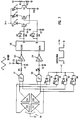
- Figure 7 shows the sensor assembly interface circuitry in accordance with this embodiment of the invention.
- Figure 7 shows additional detail not included in the simplified schematic shown in Figure 5.
- the waveforms related to Figure 7 are shown in Figure 8.
- Figure 7 shows how the active pair of electrodes is selected.
- a given pair of diagonal electrodes for example, 21A and 21C
- sensor electrode 21A will reach the threshold voltage V T before electrode 21C
- electrode 21C the active element of the diagonal electrode pair 21A, 21C
- electrode 21D will reach the threshold voltage V T before electrode 21B.
- the two active electrodes, 21B and 21C are then controlling when the output signals of the gates U1, U2 go to zero.
- the non-active electrodes, 21A and 21D have already reached the threshold voltage at time T1 and are waiting for electrodes 21B and 21C to 'catch up' at times T2 and T3.
- the other positions of the sensor assembly 20 as shown in Figures 4A through 4D operate in a similar manner.
- the two sensor electronics output signals of gates U1 and U2 are processed as follows to provide meaningful information for the user of the device.
- the two output signals from U1 and U2 are respectively the data and clock inputs of a conventional D-type flip-flop U5.
- the clock signal is inverted, as the flip-flop U5 clocks, or triggers, on the rising edge of the clock signal and the sensor electronics output signal goes to zero, or falls, when the electrode voltage reaches threshold.
- Inverter U3 inverts the output signal of gate U1 to provide the desired polarity signal.
- the propagation delay of the clock signal path must be matched in the data signal path so that the clock and data signal edges will occur at the same time when the active electrode capacitances are equal.
- the clock signal is time delayed by the R-C network of resistor R5 and capacitor C1.
- a similar delay is formed in the data signal path due to resistor R6 and capacitor C2.
- Resistor R6 is a variable resistor so that the delay in the data path has a range that is both less than and greater than the clock signal delay and can be adjusted to exactly equalize the two paths.
- the output signals Q, Q ⁇ of the flip-flop U5 thus indicate the sensor assembly's direction from level. No indication of a level condition exists yet, however, because even a very slight deviation from level may result in the clock and data signal edges not coinciding in time.
- a ten arc minute inclination 'window' is developed. This is done by 'dithering', or wiggling, the clock signal input to the flip-flop U5 with respect to the data signal.
- the flip-flop U5 will continue to change state as the clock signal is early and then late with respect to the data signal.
- a 10 arc minute inclination window is established.
- Figure 9 illustrates this operation. If the data signal edge occurs in Region One, the flip-flop U5 will always be in a 1's state and if the data edge is in Region 3, the flip-flop U5 will always be in a 0's state. However, if the data edge occurs in Region Two, the clock signal edge will sometimes occur before the data signal edge and sometimes after, resulting in the flip-flop U5 repeatedly changing state.
- the dither frequency is completely independent and non-coherent with respect to the sensor excitation voltage V E frequency.
- the preferred method of dithering the clock signal involves slightly modifying the delay time into the Schmitt gate U3 (see Figure 7) with a sawtooth dither signal provided through resistor R7.
- the dither signal is alternating current coupled via capacitor C3 so that any average direct current in the dither signal will not affect the delay time.
- Resistor R7 is preferably a variable resistor so that the amount of dither signal injected may be adjusted.
- the output signals (both Q and Q ⁇ ) of the flip-flop U5 are filtered by constantly discharging the capacitors C4 and C5 through diodes D5 and D6, which keeps transistors Q1 and Q2 turned off. With transistors Q1 and Q2 off, transistor Q3 will be on, turning on a green level indicator LED D9 (light emitting diode) in the preferred embodiment. If the flip-flop U5 remains constant in either a 0 or 1 state, the appropriate capacitor (either C4 or C5) will charge through either resistor R8 or R9.
- a conventional differential comparator circuit including transistors Q1, Q2 and Q3, and collector loads comprised of LED's D7, D8 and D9.
- Each LED D7, D8, and D9 is connected to voltage supply V++ and also respectively connected to transistors Q1, Q2, and Q3, so that a sharp on-off transition occurs at the boundaries of the dither window, resulting in a clean 'snap' action of the indicator LED's.
- Resistors R11 and R12 set the threshold voltage at which the change from a level to non-level indication occurs and resistor R10 sets the LED current. Note that only one LED D7, D8, D9 can be on at a time.
- Resistors Capacitors R1 100K ohms C1 22 pF
- R2 100K ohms C2 22 pF
- R3 100K ohms C3 .1 ⁇ F
- R4 100K ohms C4 .1 ⁇ F
- R5 2K ohms C5 .1 ⁇ F
- R6 5K ohms (variable)
- R7 50K ohms (variable)
- R9 220K ohms
- R10 150K ohms
- R12 100K ohms
- Figures 10A through 10G depict eight rotational positions for the four sensor electrodes 21A, 21B, 21C, 21D and the surface 26B of conductive fluid 26 for another embodiment of the invention.
- the appropriate pair of sensor electrodes are utilized for output signal indication.
- the required electrode pair to measure inclination is 21A and 21B
- in Figure 10F the required electrode pair to measure inclination is 21A and 21C.
- the eight positions shown in Figures 10A to 10H thus provide an indication of level relative to the sensor assembly in 45° increments.
- a conventional four element A.C. bridge is formed by the two capacitances of the sensor electrode assembly and two impedance elements which can be resistive, capacitive, inductive, or a combination thereof.
- the bridge is excited by an A.C. source.
- the two impedance elements have equal impedance.
- the A.C. voltages at two points in the bridge, each point being between one of the capacitive elements and one of the impedance elements will be equal in phase and magnitude.
- a differential amplifier having these two A.C. voltages as its input signal will then have no output signal voltage.
- the two A.C. voltages When the sensor assembly is inclined so as to unbalance the two capacitances, the two A.C. voltages will be unequal, producing a voltage at the output terminal of the differential amplifier; this voltage will be proportional to the amount of inclination.
- the phase of the output signal of the differential amplifier will be in or out of phase with regard to the A.C. excitation source, and so the phase will depend on whether the angle of inclination is greater than or less than ninety degrees, thus providing information as to the direction of inclination from level.
- One embodiment of the invention includes a machined or cast metallic housing which is the common electrode for the sensor assembly, and a conductive ring surrounding the dielectrically isolated, individual electrodes in the same plane, and electrically connected to the common electrode and electrically exposed to the conductive fluid. This significantly reduces initial sensor assembly inaccuracies due to a relative positioning shift between the sensor housing and the planar electrode assembly during assembly causing unequal volumetric path lengths through the conductive fluid from the area over the two isolated, wetted electrodes to the common electrode.
- the insulating material covering the separate, sensing electrodes is polypropylene.
- Additional stability benefits are provided by yet another embodiment having a ceramic substrate with metallic electrodes deposited on one surface and then covered with a glass-based material to form the dielectric in another embodiment.
- the conformal, glass dielectric coating will have a low adsorption and leakage rate via osmosis with the additional benefit of an excellent surface finish.
- the recovery time of the fluid within the sensor cavity after a physical disturbance is subject to the surface finish of the dielectric. As the disturbed fluid flows down the face of the dielectric toward the majority of the fluid in the bottom of the reservoir, the time required depends upon the microscopic obstacles the fluid encounters on the dielectric surface in the form of surface deformities. Hence the smoother the surface, the more rapid and consistent the recovery time.
- Figure 11A shows an exploded view of a sensor assembly including circuit board 40 with an etched sensor pattern with straight-sided sensor electrodes 42a, 42b, 42c, 42d and conductive ring 44 which when assembled is covered with polypropylene film 46 as a dielectric.
- a metal cover 50 (shown partially cut away) is fastened to circuit board 40 by screws through mounting holes 52a, 52b, 52c.
- Metal cover 50 is machined or die cast from aluminum or zinc alloy.
- O-ring 54 is held in a groove (not shown) in metal cover 50.
- a second metal cover (not shown) is provided on the backside of substrate 40, having threaded holes mating with the mounting holes in metal cover 50.
- Figure 11B shows a cross section of the sensor assembly of Figure 11A. Shown are substrate (circuit board) 40, electrodes 42c, 42d, common conductive ring 44, metal cover 50, O-ring 54, dielectric film 46, and conductive fluid 58. Conductive fluid 58 is 99% anhydrous isopropyl alcohol and 1% water.
- Figure 12a shows another sensor assembly also in accordance with the invention as described above using a ceramic substrate with deposited thick film electrodes and a glass-based dielectric. Shown are ceramic substrate 62 with common ring metallization 64 deposited thereon and electrodes 66a, 66b, 66c, 66d, deposited thereon.
- the dielectric 68 is glass-based and its outer periphery is shown by a dotted line, so it covers electrodes 66a, 66b, 66c, 66d.
- the second dotted line shows to where the boundary of the inner wall of the metal cover 70 extends. Holes 72a, 72b, 72c, 72d are provided to fasten substrate 62 by screws (not shown) which extend into matching threaded holes in metal cover 70.
- Figure 12B shows a cross section through line A-A' of Figure 12A. Shown are metal cover 70, fluid reservoir 76, and substrate 62. Also shown are via holes 78a, 78b for electrode connections to electrode 66c, 66b, respectively.
- Figure 12C shows an enlarged view of the circled area 80 in Figure 12B. Shown are metal cover 70, common ring 64, electrode 66c, dielectric 68, and substrate 62. Distance A is 0.030 inches (0.76 mm), and distance B is 0.015 to 0.020 inches (.38 to .51 mm). The advantage of this structure is that a slight misalignment of cover 70 on substrate 62, affecting distance C, will not alter the accuracy of the instrument. In this embodiment, cover 70 is sealed to substrate 62 at location 82 by eutectic solder or alcohol impervious epoxy, and no second metal cover is needed on the backside 84 of substrate 62.
- individual, differential input voltage comparators are used instead of Schmitt triggers. This allows use of a single voltage reference for comparison with the electrode signals, thus providing a common reference level whose voltage is not pre-established as in the case of the Schmitt trigger's, but is individually tailored to yield optimum performance.
- the amplitude "dither" voltage utilized to establish a known band of level or plumb condition is injected along with the reference voltage into the appropriate comparators. Utilizing a single stage to convert from the analog output of any sensor element to a digital type signal for subsequent processing is advantageous.
- each operating position of the sensor unit is individually calibrated.
- environmental effects such as temperature
- FIG 13 shows a simplified circuit diagram of the basic sensor electronics in this embodiment with only a single pair of active electrodes C1, C2 shown for simplicity.
- comparators U1 and U2 will then change state at the same time. If, however, capacitors C1, C2 are not the same value (as in Figure 14, i.e., the sensor assembly is not level) then the sensor electrode with the lower capacitance will charge quicker and reach the reference voltage before the other electrode circuit. The outputs of capacitors U1, U2 will not change at the same time and this time difference (t2-t1) is used to indicate an out-of-level or unbalanced condition. A longer low output or "zero" time for V E ensures that capacitors C1, C2 are fully discharged before starting a new cycle. The duty curve of V E is typically 5%.
- Figures 13 and 15 show the logic of one embodiment of the invention.
- the comparator outputs for a given pair of diagonal electrodes selected from electrodes A, B, C, D are connected to the inputs of an AND gate (for example, U5), with the other diagonal electrode pair B and D similarly connected.
- Electrodes B and C are the active electrodes, in which case electrode A will reach the reference voltage V R before electrode C, and when C (the active element of the diagonal pair) does reach threshold, the output of U5 will go high.
- Figure 16A shows the associated waveforms, with Figure 16B showing the electrode configuration and orientation relative to the conductive fluid associated with the wave forms of Figure 16A.
- electrode D will reach threshold before B.
- the two active electrodes, B and C, are then controlling when the outputs of the AND gates, U5 and U6, go high.
- the non-active electrodes, A and D reach the reference voltage at time tl and their associated comparator outputs are then at a one level, waiting for B and C to "catch up" at times t2 and t3, at which times the AND gate outputs of U5 and U6 go high.
- the other positions of the sensor assembly (as shown in Figures 4A through 4D) operate in a similar manner.
- a ten arc minute “window” is developed. This is done by “dithering", or wiggling, the Clock signal to flip-flop U9 in time with respect to the Data signal. If the Data signal to flip-flop U9 is within the dithering window of the Clock, flip-flop U9 will continue to change state between "1" and "0" as the Clock signal is sometimes early and sometimes late with respect to the Data signal. By adjusting the amount of time dither, a 10' window can be established. Figure 17 illustrates this. If the Data edge occurs in Region One, flip-flop U9 will always be in a 0's state and if the Data edge is in Region Three, the flip-flop will always be in a 1's state.
- the dither frequency is independent and non-coherent with the sensor assembly excitation frequency, V E .
- Dithering of the Clock signal is achieved by slightly modifying the threshold voltage into comparators U1 and U3 with a low level sawtooth waveform.
- the dithering signal is AC coupled via capacitors C1 and C2 so that any average direct current on the dither signal will not affect the average reference voltage.
- the outputs (both Q and Q ⁇ ) of flip-flop U9 are filtered by constantly discharging the capacitors C3 and C4 through diodes D1 and D2, which keeps transistors Q1 and Q3 turned off. With transistors Q1 and Q3 off, transistor Q2 will be on, turning on the green level indicator LED, D4.
- flip-flop U9 remains constant in either a 0 or a 1 state (indicating an out-of-level condition)
- the appropriate capacitor either C3 or C4 will charge through either resistor R14 or R15 and as the base of either transistor Q1 or Q3 reaches the same voltage as transistors Q2's base, transistor Q1 or Q3 will start to turn on, and as the base voltage increases to 5V (the flip-flop outputs' 1 level), transistor Q2 will be turned off entirely.
- Resistors R16 and R17 set the threshold at which the change from a level to un-level condition occurs and resistor R18 sets the LED D3, D4, D5 current (note that the circuit allows only one LED to be on at a time.)
- Gates U7 and U8 along with flip-flop U10 comprise a detector for the Inverted Plumb mode (sensor elements C and D active).
- Figure 18 illustrates this logic.
- Figure 18, Part A shows each sensor's delay time on one axis versus the inclination angle (or rotational angle) of the entire sensor array on the other axis.
- each of the comparator outputs associated with the individual electrodes will have a varying time delay between the 'zero' to 'one' edge transition of the excitation voltage, V E and the edge transition of any one comparator's output. If, for example, a given electrode has no fluid coverage (is unwetted), this delay time will be minimal. If however, the given electrode has some fluid coverage, the delay time will increase from the minimum value, and as the maximum percentage of wetted electrode area is reached, the delay time will be at the maximum achievable. Note that the maximum time delay achievable does not correspond to the null, or equal capacitance values for any given active or wetted electrode pair.
- sensor comparator outputs C and D have longer delay times than do A and B.
- This region can be uniquely detected by logically AND'ing signal A with B by logic gate U7 and logically OR'ing signal C with D by logic gate U8.
- the output of gate U7 will have a longer delay than gate U8 only in this region.
- gates U7 and U8 are processed in an identical way as the main signal processing is done (by gates U5 and U6) to detect the direction of out-of-level condition.
- gate U7 is the Clock signal to a D-type flip-flop, U10
- gate U8's output is the Data signal.
- the Data input to flip-flop U10 from gate U8 will be a one at the time of the Clock edge from gate U7, thus setting flip-flop U10 to a one state (as shown in Figure 18, Part C).
- flip-flop U10 being set to a zero state, as shown in Figure 18, Parts B and D.
- a normally unused feature of a D-type flip-flop is used. If both Set and Reset inputs are high at the same time, both Q and Q ⁇ outputs will be high. This will cause both High and Low out-of-level LED's to be on (D3 and D5 of Figure 15) and will not allow a conventional, visual output associated with normal operating positions (a single LED on at at time).
- the Q output of flip-flop U10 is connected to the Set and Reset inputs of flip-flop U9 to provide this action. When the level exits the Inverted Plumb mode, normal operation automatically resumes.
- a low battery indication provided in accordance with the invention also utilizes the above feature of a D-type flip-flop. If a low battery sensor deriving a logic type signal is connected with the correct logic sense to flip-flop U10's set input such that when a low battery condition exists, flip-flop U10 will be set to a "1", causing both High and Low LED's to be on simultaneously. Normal operation is precluded, as no normal operating indication can be obtained.
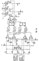
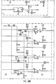
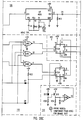
- Figure 19A shows the entire level device in block diagram form. Shown are battery 100, power switch 102, five volt regulator 104, auto-off counter 106, excitation voltage generator 108, dither voltage generator 110, sensor assembly 112, sensor voltage comparator 114, calibration circuit 116, electrode pair auto select logic 118, low battery detector 120, signal processing circuitry 122, lowpass filters 124, 126, display LED drivers 128, LED's 130, and beeper driver 132 for driving beeper 134. Note that auto-off counter 106 automatically turns the device off if the sensors 112 are electrically quiescent for a predetermined period such as two minutes.
- Power switch 102 has several advantageous features including a single, non-mechanical latching switch controlling both on and off functions; no standby power drain when off; and input for remote off signal.
- voltage V 1 is 9V and voltage V 2 is 0V.
- the charge on capacitor C1 is zero.
- switch SW1 When switch SW1 is closed, the voltage across capacitor C1 will still be zero, but current will flow through the circuit resistor R1, R2, capacitor C1 and resistor R4, turning on transistor Q2. This in turn on transistor Q1.
- resistor R1, R2, capacitor C1 and resistor R4 turning on transistor Q2. This in turn on transistor Q1.
- additional base current to transistor Q2 will flow through resistor R6, latching the circuit on.
- Remote off capability is provided via transistor Q3 which, when turned on, removes all base drive from transistor Q2, thus turning the switch off.
- Capacitor C2 on the base of transistor Q3 provides charge retention to keep transistor Q3 on as the remote off signal is removed insuring reliable circuit turn-off.
- Figure 20 illustrates schematically one embodiment of the entire device as shown in Figure 19A, with the blocks of Figure 19A outlined with dotted lines and labeled with the reference numbers of Figure 18.
Landscapes
- Physics & Mathematics (AREA)
- Engineering & Computer Science (AREA)
- General Physics & Mathematics (AREA)
- Radar, Positioning & Navigation (AREA)
- Remote Sensing (AREA)
- Measurement Of Levels Of Liquids Or Fluent Solid Materials (AREA)
- Investigating Or Analyzing Materials By The Use Of Electric Means (AREA)
Claims (9)
- Kapazitive Neigungsfühlervorrichtung (20) umfassend:eine in elektrischem Kontakt mit einer ersten Elektrode (28) befindliche leitfähige Flüssigkeit (26), wobei die leitfähige Flüssigkeit eine Oberfläche hat;eine zweite, dritte, vierte und fünfte Elektrode (21A, 21B, 21C, 21D), die jeweils von einer dielektrischen Schicht (22) bedeckt ist und neben der Oberfläche der leitfähigen Flüssigkeit liegt;logisches Mittel für die automatische Auswahl einer ersten und einer zweiten aktiven Elektrode aus der zweiten, dritten, vierten und fünften Elektrode (21A, 21B, 21C, 21D);ein erster und ein zweiter elektrischer Widerstand (R1, R2, R3, R4), die jeweils mit der ersten bzw. der zweiten aktiven Elektrode in Reihe geschaltet werden;erste Mittel (U1; U1, U2) zum Verwenden einer zyklisch variierenden Spannung zum Bestimmen einer ersten Ladezeit einer Schaltung, die den ersten Widerstand und die Kapazität zwischen der ersten Elektrode und der ersten aktiven Elektrode einschließt;zweite Mittel (U2; U3, U4) zum Verwenden der zyklisch variierenden Spannung zum Bestimmen einer zweiten Ladezeit einer Schaltung, die den zweiten Widerstand und die Kapazität zwischen der ersten und der zweiten aktiven Elektrode einschließt; undMittel (U5; U5, U6, U9) zum Vergleichen der ersten und zweiten Ladezeit, um eine Neigung der Vorrichtung in einem Zyklus variierender Spannung zu bestimmen.
- Vorrichtung nach Anspruch 1, wobei das Mittel zum Vergleichen (U5; U5, U6, U9) ein Nullsensor zum Abtasten eines Zustands des Geräts ist, wobei der Zustand etwa parallel oder senkrecht zur Schwerkraftrichtung ist, indem gleiche Ladezeiten auf einen vorbestimmten Spannungspegel mit dem ersten (U1; U1, U2) und dem zweiten (U2, U3, U4) Mittel zum Bestimmen bestimmt werden, und wobei ein Mittel (R7) zum verstellbaren Bestimmen einer Reihe von Neigungen der Vorrichtung vorgesehen ist, an der der Zustand abgetastet wird.
- Vorrichtung nach Anspruch 2, wobei das Mittel zum verstellbaren Bestimmen der Reihe von Neigungen eine bistabile Kippschaltung mit einem Dateneingangsanschluß und einem Uhrenanschluß aufweist, wobei der Dateneingangsanschluß mit dem Mittel zum Vergleichen verbunden ist und der Uhreneingangsanschluß mit einer Quelle variierender Spannung verbunden ist, wodurch eine verstellbare Änderung der Ladezeit vorgesehen wird.
- Vorrichtung nach Anspruch 1, wobei das Mittel zum Vergleichen erste (U5, U7) und zweite (U6, U8) Verknüpfungsglieder mit an einen Ausgangsanschluß des ersten (U1, U2) beziehungsweise des zweiten (U3, U4) Mittels zum Bestimmen angeschlossenen Eingangsanschlüssen, Mittel zum Anlegen einer veränderlichen Zitterspannung an das erste und zweite Mittel zum Bestimmen, wodurch eine verstellbare Änderung der Ladezeit vorgesehen wird, und eine bistabile Kippschaltung (U9, U10) mit einem Dateneingangsanschluß und einem Uhrenanschluß umfaßt, welche an die Ausgangsanschlüsse des ersten beziehungsweise zweiten Verknüpfungsglieds angeschlossen sind.
- Vorrichtung nach Anspruch 1, 2, 3 oder 4, wobei das erste (U1, U2) und zweite (U3, U4) Mittel zum Bestimmen durch Abtasten eines Bezugsspannungspegels über die Kapazität jeweils die Ladezeit bestimmen, und ferner umfassend Mittel zum Variieren des von jedem Mittel zum Bestimmen abgetasteten Bezugsspannungspegels.
- Vorrichtung nach einem der vorangehenden Ansprüche, wobei die erste Elektrode (28) eine erste ebene Oberfläche hat, und wobei die zweite, dritte, vierte und fünfte Elektrode (21A, 21B, 21C, 21D) auf einer zweiten ebenen Oberfläche parallel zur ersten ebenen Oberfläche geformte und mit Zwischenraum dazu angeordnete Quadranten sind.
- Vorrichtung nach einem der vorangehenden Ansprüche, umfassend einen dritten und einen vierten elektrischen Widerstand, der mit der vierten beziehungsweise fünften Elektrode in Reihe geschaltet ist, ein drittes Mittel zum Bestimmen einer Ladezeit einer Schaltung einschließlich dem dritten Widerstand und der Kapazität zwischen der ersten und der vierten Elektrode, ein viertes Mittel zum Bestimmen einer Ladezeit einer Schaltung einschließlich dem vierten Widerstand und der Kapazität zwischen der ersten und der fünften Elektrode, und wobei das Mittel zum automatischen Auswählen von zwei der Elektroden ein erstes Verknüpfungsglied mit zwei Eingangsanschlüssen, die zum Empfangen von Ausgangssignalen von dem ersten beziehungsweise dritten Mittel zum Bestimmen angeschlossen sind, ein zweites Verknüpfungsglied mit zwei Eingangsanschlüssen, die zum Empfangen von Ausgangssignalen von dem zweiten und vierten Mittel zum Bestimmen angeschlossen sind, und eine bistabile Kippschaltung aufweist, deren Uhrenanschluß und Dateneingangsanschluß zum Empfangen von Ausgangssignalen vom ersten beziehungsweise zweiten Verknüpfungsglied angeschlossen sind, wodurch eine Datenanschlußeinheit der bistabilen Kippschaltung auf die automatische Auswahl von zweien der Elektroden hin ein Signal vorsieht.
- Vorrichtung nach einem der vorangehenden Ansprüche, wobei die leitfähige Flüssigkeit (26) Alkohol und Wasser umfaßt, die zweiten und dritten Elektroden (21A, 21B, 21C, 12D) auf einem Keramiksubstrat (32) geformt sind und die dielektrischen Schichten (22) ein Glasmaterial sind.
- Verfahren zur Neigungsmessung umfassend die folgenden Schritte:Vorsehen einer in elektrischem Kontakt mit einer ersten Elektrode (28) befindlichen leitfähigen Flüssigkeit (26), wobei die leitfähige Flüssigkeit eine Oberfläche hat;Vorsehen einer zweiten, dritten, vierten und fünften Elektrode (21A, 21B, 21C, 21D), die jeweils von einer dielektrischen Schicht (22) bedeckt ist und neben der Oberfläche der leitfähigen Flüssigkeit liegt;Vorsehen eines logischen Mittels für die automatische Auswahl einer ersten und einer zweiten aktiven Elektrode aus der zweiten, dritten, vierten und fünften Elektrode (21A, 21B, 21C, 21D);Anschließen eines ersten Widerstands (R2, R3) in Reihe mit der ersten aktiven Elektrode und eines zweiten elektrischen Widerstands (R1, R4) in Reihe mit der zweiten aktiven Elektrode;Verwenden einer zyklisch variierenden Spannung zum Bestimmen einer ersten Ladezeit des ersten Widerstands und der Kapazität zwischen der ersten Elektrode und der ersten aktiven Elektrode einschließt, und Verwenden der zyklisch variierenden Spannung zum Bestimmen einer zweiten Ladezeit des zweiten Widerstands und der Kapazität zwischen der ersten Elektrode und der zweiten aktiven Elektrode; undVergleichen der ersten und zweiten Ladezeit, um eine Neigung der Vorrichtung zu bestimmen, wobei die Neigung der Vorrichtung in einem Zyklus der variierender Spannung bestimmt wird.
Applications Claiming Priority (5)
| Application Number | Priority Date | Filing Date | Title |
|---|---|---|---|
| US32658689A | 1989-03-21 | 1989-03-21 | |
| US326586 | 1989-03-21 | ||
| US48664390A | 1990-02-28 | 1990-02-28 | |
| PCT/US1990/001487 WO1990011489A1 (en) | 1989-03-21 | 1990-03-20 | Electronic capacitive level with automatic electrode selection |
| US486643 | 1995-06-07 |
Publications (3)
| Publication Number | Publication Date |
|---|---|
| EP0464145A1 EP0464145A1 (de) | 1992-01-08 |
| EP0464145A4 EP0464145A4 (en) | 1993-03-03 |
| EP0464145B1 true EP0464145B1 (de) | 1996-07-17 |
Family
ID=26985467
Family Applications (1)
| Application Number | Title | Priority Date | Filing Date |
|---|---|---|---|
| EP90905895A Expired - Lifetime EP0464145B1 (de) | 1989-03-21 | 1990-03-20 | Elektronische kondensatorwasserwaage mit selbsttätiger elektrodenauswahl |
Country Status (5)
| Country | Link |
|---|---|
| EP (1) | EP0464145B1 (de) |
| AU (1) | AU5358090A (de) |
| CA (1) | CA2049963C (de) |
| DE (1) | DE69027851T2 (de) |
| WO (1) | WO1990011489A1 (de) |
Cited By (2)
| Publication number | Priority date | Publication date | Assignee | Title |
|---|---|---|---|---|
| CN104034308A (zh) * | 2014-04-28 | 2014-09-10 | 哈尔滨工业大学 | 同心共面二等分环-二等分圆嵌套极板倾角测量方法与装置 |
| CN104034313A (zh) * | 2014-04-28 | 2014-09-10 | 哈尔滨工业大学 | 同心共面环-三等分环-圆嵌套极板倾角测量方法与装置 |
Families Citing this family (12)
| Publication number | Priority date | Publication date | Assignee | Title |
|---|---|---|---|---|
| US5259118A (en) * | 1989-03-21 | 1993-11-09 | Zircon Corporation | Electronic capacitive level with display showing direction of rotation to achieve level/plumb |
| US5174033A (en) * | 1990-06-18 | 1992-12-29 | The Charles Machine Works, Inc. | Angle sensor for a steerable boring tool |
| EP0492330A1 (de) * | 1990-12-24 | 1992-07-01 | Deutsche Aerospace AG | Kapazitiver Neigungssensor |
| IL100345A0 (en) * | 1991-12-11 | 1992-09-06 | Israel State | Inclinometer |
| US5313713A (en) * | 1992-08-14 | 1994-05-24 | Zircon Corporation | Electronic level with display scale and audible tone scale |
| US5479716A (en) * | 1994-07-12 | 1996-01-02 | Design & Test Technology, Inc. | Capacitive based gravity sensor |
| WO1996004524A1 (en) * | 1994-08-01 | 1996-02-15 | Nofa Industrial Oy | Method for compensating measuring errors in inclination sensor |
| US5956260A (en) * | 1996-08-09 | 1999-09-21 | Zircon Corporation | Electronic level displaying inclination having digital and analog displays |
| US5852878A (en) * | 1997-07-14 | 1998-12-29 | The Fredericks Company | Electrolytic tilt sensing device |
| FR2793317B1 (fr) * | 1999-05-06 | 2001-07-13 | Daniel Roux | Dispositif de mesure de la variation de position entre deux referentiels de positionnement situes a des altitudes differentes |
| JP3659855B2 (ja) * | 2000-02-25 | 2005-06-15 | 株式会社タイコーデバイス | 傾斜センサ |
| EP1162466A1 (de) * | 2000-06-06 | 2001-12-12 | Product Innovation Holdings Limited | Bewegungsaufnehmer |
Family Cites Families (14)
| Publication number | Priority date | Publication date | Assignee | Title |
|---|---|---|---|---|
| US2936411A (en) * | 1955-11-29 | 1960-05-10 | Robert O Doty | Tilt sensitive multiple capacitor device |
| US4077132A (en) * | 1977-02-22 | 1978-03-07 | Keuffel & Esser Company | Digital level indicator |
| US4167818A (en) * | 1978-02-03 | 1979-09-18 | Robert Cantarella | Electronic inclination gauge |
| GB2070774A (en) * | 1980-02-28 | 1981-09-09 | Pa Management Consult | Capactive clinometer |
| CH660522A5 (de) * | 1981-10-02 | 1987-04-30 | Geotronics Ab | Elektronische nivelliervorrichtung. |
| GB2115223B (en) * | 1982-02-18 | 1985-07-10 | Standard Telephones Cables Ltd | Multilayer ceramic dielectric capacitors |
| US4574491A (en) * | 1984-07-27 | 1986-03-11 | Vining Russell W | Level with audio indicator |
| JPS61126414A (ja) * | 1984-11-24 | 1986-06-13 | Tokyo Optical Co Ltd | 傾斜角測定装置 |
| US4642555A (en) * | 1985-01-31 | 1987-02-10 | Sperry Corporation | Differential capacitance detector |
| US4644662A (en) * | 1985-01-31 | 1987-02-24 | Sperry Corporation | Capacitive gravity sensor |
| US4622619A (en) * | 1985-03-13 | 1986-11-11 | Rogers Corporation | Decoupling capacitor and method of manufacture thereof |
| GB2186693B (en) * | 1986-01-23 | 1990-09-05 | Duracell Int | Inclination sensor |
| DD272781A3 (de) * | 1987-04-24 | 1989-10-25 | Weinert E Messgeraetewerk | Kapazitiver neigungssensor |
| JPS649309A (en) * | 1987-07-01 | 1989-01-12 | Agency Ind Science Techn | Electrostatic capacitance type angle of inclination sensor |
-
1990
- 1990-03-20 WO PCT/US1990/001487 patent/WO1990011489A1/en not_active Ceased
- 1990-03-20 AU AU53580/90A patent/AU5358090A/en not_active Abandoned
- 1990-03-20 EP EP90905895A patent/EP0464145B1/de not_active Expired - Lifetime
- 1990-03-20 DE DE69027851T patent/DE69027851T2/de not_active Expired - Fee Related
- 1990-03-20 CA CA002049963A patent/CA2049963C/en not_active Expired - Fee Related
Cited By (4)
| Publication number | Priority date | Publication date | Assignee | Title |
|---|---|---|---|---|
| CN104034308A (zh) * | 2014-04-28 | 2014-09-10 | 哈尔滨工业大学 | 同心共面二等分环-二等分圆嵌套极板倾角测量方法与装置 |
| CN104034313A (zh) * | 2014-04-28 | 2014-09-10 | 哈尔滨工业大学 | 同心共面环-三等分环-圆嵌套极板倾角测量方法与装置 |
| CN104034308B (zh) * | 2014-04-28 | 2016-07-06 | 哈尔滨工业大学 | 同心共面二等分环-二等分圆嵌套极板倾角测量方法与装置 |
| CN104034313B (zh) * | 2014-04-28 | 2016-08-24 | 哈尔滨工业大学 | 同心共面环-三等分环-圆嵌套极板倾角测量方法与装置 |
Also Published As
| Publication number | Publication date |
|---|---|
| AU5358090A (en) | 1990-10-22 |
| EP0464145A1 (de) | 1992-01-08 |
| EP0464145A4 (en) | 1993-03-03 |
| CA2049963C (en) | 2001-08-28 |
| DE69027851D1 (de) | 1996-08-22 |
| CA2049963A1 (en) | 1990-09-22 |
| WO1990011489A1 (en) | 1990-10-04 |
| DE69027851T2 (de) | 1997-03-20 |
Similar Documents
| Publication | Publication Date | Title |
|---|---|---|
| US5083383A (en) | Electronic capacitance level with automatic electrode selection | |
| CA2049963C (en) | Electronic capacitive level with automatic electrode selection | |
| US4943889A (en) | Electrostatic capacitor type sensing device | |
| EP0291507B1 (de) | Elektronisches neigungsmessgerät | |
| US4528760A (en) | Clinometer | |
| CA1286746C (en) | Two-axis differential capacitance inclinometer | |
| KR100218899B1 (ko) | 2축 경사 센서 | |
| US4510436A (en) | Dielectric measuring systems | |
| US4644662A (en) | Capacitive gravity sensor | |
| US6802132B1 (en) | Electrolytic tilt sensor and method for manufacturing same | |
| WO1999010714A1 (en) | A compensated capacitive liquid level sensor | |
| EP0243011B1 (de) | Elektronischer Neigungsmesser | |
| KR910004509Y1 (ko) | 알코올 센서 | |
| US3946494A (en) | Toroidal electrolytic angle transducer | |
| US5852878A (en) | Electrolytic tilt sensing device | |
| US5479716A (en) | Capacitive based gravity sensor | |
| JP3385158B2 (ja) | 傾斜センサ | |
| US4354219A (en) | Capacitance sensing device | |
| EP0190832B1 (de) | Neigungsmesser | |
| JP2003057093A (ja) | 液面レベル検出器用電極 | |
| US4789822A (en) | Three-electrode sensor for phase comparison and pulse phase adjusting circuit for use with the sensor | |
| US4468864A (en) | Tilt meter | |
| EP0257724A2 (de) | Wandler mit drei Elektroden für Phasenvergleich und Pulsphasenabgleichungskette zum Gebrauch mit dem Wandler | |
| EP0546822A2 (de) | Inklinometer unter Anwendung einer dielektrischen Flüssigkeit | |
| JPH06147955A (ja) | 静電容量式レベルセンサ |
Legal Events
| Date | Code | Title | Description |
|---|---|---|---|
| PUAI | Public reference made under article 153(3) epc to a published international application that has entered the european phase |
Free format text: ORIGINAL CODE: 0009012 |
|
| 17P | Request for examination filed |
Effective date: 19910920 |
|
| AK | Designated contracting states |
Kind code of ref document: A1 Designated state(s): CH DE FR GB IT LI NL SE |
|
| A4 | Supplementary search report drawn up and despatched |
Effective date: 19930111 |
|
| AK | Designated contracting states |
Kind code of ref document: A4 Designated state(s): CH DE FR GB IT LI NL SE |
|
| 17Q | First examination report despatched |
Effective date: 19931108 |
|
| GRAH | Despatch of communication of intention to grant a patent |
Free format text: ORIGINAL CODE: EPIDOS IGRA |
|
| GRAH | Despatch of communication of intention to grant a patent |
Free format text: ORIGINAL CODE: EPIDOS IGRA |
|
| GRAA | (expected) grant |
Free format text: ORIGINAL CODE: 0009210 |
|
| AK | Designated contracting states |
Kind code of ref document: B1 Designated state(s): CH DE FR GB IT LI NL SE |
|
| PG25 | Lapsed in a contracting state [announced via postgrant information from national office to epo] |
Ref country code: NL Free format text: LAPSE BECAUSE OF FAILURE TO SUBMIT A TRANSLATION OF THE DESCRIPTION OR TO PAY THE FEE WITHIN THE PRESCRIBED TIME-LIMIT Effective date: 19960717 Ref country code: LI Effective date: 19960717 Ref country code: CH Effective date: 19960717 |
|
| ITF | It: translation for a ep patent filed | ||
| REF | Corresponds to: |
Ref document number: 69027851 Country of ref document: DE Date of ref document: 19960822 |
|
| ET | Fr: translation filed | ||
| PG25 | Lapsed in a contracting state [announced via postgrant information from national office to epo] |
Ref country code: SE Effective date: 19961017 |
|
| NLV1 | Nl: lapsed or annulled due to failure to fulfill the requirements of art. 29p and 29m of the patents act | ||
| REG | Reference to a national code |
Ref country code: CH Ref legal event code: PL |
|
| PLBE | No opposition filed within time limit |
Free format text: ORIGINAL CODE: 0009261 |
|
| STAA | Information on the status of an ep patent application or granted ep patent |
Free format text: STATUS: NO OPPOSITION FILED WITHIN TIME LIMIT |
|
| 26N | No opposition filed | ||
| REG | Reference to a national code |
Ref country code: FR Ref legal event code: CD |
|
| PGFP | Annual fee paid to national office [announced via postgrant information from national office to epo] |
Ref country code: FR Payment date: 20010302 Year of fee payment: 12 |
|
| PGFP | Annual fee paid to national office [announced via postgrant information from national office to epo] |
Ref country code: GB Payment date: 20010306 Year of fee payment: 12 |
|
| PGFP | Annual fee paid to national office [announced via postgrant information from national office to epo] |
Ref country code: DE Payment date: 20010307 Year of fee payment: 12 |
|
| REG | Reference to a national code |
Ref country code: GB Ref legal event code: IF02 |
|
| PG25 | Lapsed in a contracting state [announced via postgrant information from national office to epo] |
Ref country code: GB Free format text: LAPSE BECAUSE OF NON-PAYMENT OF DUE FEES Effective date: 20020320 |
|
| PG25 | Lapsed in a contracting state [announced via postgrant information from national office to epo] |
Ref country code: DE Free format text: LAPSE BECAUSE OF NON-PAYMENT OF DUE FEES Effective date: 20021001 |
|
| GBPC | Gb: european patent ceased through non-payment of renewal fee |
Effective date: 20020320 |
|
| PG25 | Lapsed in a contracting state [announced via postgrant information from national office to epo] |
Ref country code: FR Free format text: LAPSE BECAUSE OF NON-PAYMENT OF DUE FEES Effective date: 20021129 |
|
| REG | Reference to a national code |
Ref country code: FR Ref legal event code: ST |
|
| PG25 | Lapsed in a contracting state [announced via postgrant information from national office to epo] |
Ref country code: IT Free format text: LAPSE BECAUSE OF NON-PAYMENT OF DUE FEES Effective date: 20050320 |