EP0464230A1 - Boucle d'asservissement de phase numérique - Google Patents
Boucle d'asservissement de phase numérique Download PDFInfo
- Publication number
- EP0464230A1 EP0464230A1 EP90112531A EP90112531A EP0464230A1 EP 0464230 A1 EP0464230 A1 EP 0464230A1 EP 90112531 A EP90112531 A EP 90112531A EP 90112531 A EP90112531 A EP 90112531A EP 0464230 A1 EP0464230 A1 EP 0464230A1
- Authority
- EP
- European Patent Office
- Prior art keywords
- phase
- digital
- digital oscillator
- signal
- output signal
- Prior art date
- Legal status (The legal status is an assumption and is not a legal conclusion. Google has not performed a legal analysis and makes no representation as to the accuracy of the status listed.)
- Granted
Links
- 108010076504 Protein Sorting Signals Proteins 0.000 claims abstract description 20
- 238000012937 correction Methods 0.000 claims abstract description 14
- 238000012545 processing Methods 0.000 claims description 17
- 230000000737 periodic effect Effects 0.000 claims description 11
- 238000000034 method Methods 0.000 claims description 9
- 230000008569 process Effects 0.000 claims description 7
- 230000001960 triggered effect Effects 0.000 claims description 4
- 125000004122 cyclic group Chemical group 0.000 claims description 2
- 238000001914 filtration Methods 0.000 claims 1
- 238000000926 separation method Methods 0.000 description 9
- 230000002123 temporal effect Effects 0.000 description 7
- 230000000875 corresponding effect Effects 0.000 description 5
- 238000005259 measurement Methods 0.000 description 4
- 238000009825 accumulation Methods 0.000 description 3
- 230000008878 coupling Effects 0.000 description 3
- 238000010168 coupling process Methods 0.000 description 3
- 238000005859 coupling reaction Methods 0.000 description 3
- 230000000694 effects Effects 0.000 description 3
- 230000004044 response Effects 0.000 description 3
- 230000008901 benefit Effects 0.000 description 2
- 230000001276 controlling effect Effects 0.000 description 2
- 230000006870 function Effects 0.000 description 2
- 238000005070 sampling Methods 0.000 description 2
- 230000001360 synchronised effect Effects 0.000 description 2
- 230000001052 transient effect Effects 0.000 description 2
- 238000013459 approach Methods 0.000 description 1
- 238000005352 clarification Methods 0.000 description 1
- 230000000295 complement effect Effects 0.000 description 1
- 239000002131 composite material Substances 0.000 description 1
- 238000004590 computer program Methods 0.000 description 1
- 230000002596 correlated effect Effects 0.000 description 1
- 238000011161 development Methods 0.000 description 1
- 230000018109 developmental process Effects 0.000 description 1
- 230000009977 dual effect Effects 0.000 description 1
- 230000007274 generation of a signal involved in cell-cell signaling Effects 0.000 description 1
- 239000000203 mixture Substances 0.000 description 1
- 238000011144 upstream manufacturing Methods 0.000 description 1
Images


Classifications
-
- H—ELECTRICITY
- H03—ELECTRONIC CIRCUITRY
- H03L—AUTOMATIC CONTROL, STARTING, SYNCHRONISATION OR STABILISATION OF GENERATORS OF ELECTRONIC OSCILLATIONS OR PULSES
- H03L7/00—Automatic control of frequency or phase; Synchronisation
- H03L7/06—Automatic control of frequency or phase; Synchronisation using a reference signal applied to a frequency- or phase-locked loop
- H03L7/08—Details of the phase-locked loop
- H03L7/099—Details of the phase-locked loop concerning mainly the controlled oscillator of the loop
-
- H—ELECTRICITY
- H03—ELECTRONIC CIRCUITRY
- H03L—AUTOMATIC CONTROL, STARTING, SYNCHRONISATION OR STABILISATION OF GENERATORS OF ELECTRONIC OSCILLATIONS OR PULSES
- H03L7/00—Automatic control of frequency or phase; Synchronisation
- H03L7/06—Automatic control of frequency or phase; Synchronisation using a reference signal applied to a frequency- or phase-locked loop
- H03L7/08—Details of the phase-locked loop
- H03L7/099—Details of the phase-locked loop concerning mainly the controlled oscillator of the loop
- H03L7/0991—Details of the phase-locked loop concerning mainly the controlled oscillator of the loop the oscillator being a digital oscillator, e.g. composed of a fixed oscillator followed by a variable frequency divider
- H03L7/0994—Details of the phase-locked loop concerning mainly the controlled oscillator of the loop the oscillator being a digital oscillator, e.g. composed of a fixed oscillator followed by a variable frequency divider comprising an accumulator
-
- H—ELECTRICITY
- H04—ELECTRIC COMMUNICATION TECHNIQUE
- H04N—PICTORIAL COMMUNICATION, e.g. TELEVISION
- H04N9/00—Details of colour television systems
- H04N9/79—Processing of colour television signals in connection with recording
- H04N9/87—Regeneration of colour television signals
Definitions
- the invention relates to a digital phase control loop, with a periodically overflowing digital oscillator, which generates a digital oscillator output signal having the period T by incrementing a register word of the word length N successively in the predetermined clock of a clock generator by a control word applied to an input of the digital oscillator, and with a processor device, to which the digital oscillator output signal representing the actual phase of the digital oscillator is fed, and which for comparing the period T of the digital oscillator to a nominal period determined by periodically occurring synchronization pulses, a phase comparison between the actual phase of the digital oscillator and a predetermined target -Phase carried out such that the processor device in a first control cycle predetermined by the periodically occurring synchronization pulses from the current actual phase of the digital oscillator and au s of the desired phase forms a phase difference signal, and that the phase difference signal is filtered in a loop filter unit of the processor device, and that the filtered phase difference signal is added to a frequency word which is the numerical value of the
- DPLL digital phase locked loop
- the content of the register word of the digital oscillator at this trigger time is stored as the current actual phase of the digital oscillator.
- the phase comparison between the current actual phase of the digital oscillator and the predetermined target phase at this time and the tracking of the period of the digital oscillator is then carried out in the manner described above.
- the processor device therefore carries out the adjustment necessary to adjust the period T of the digital oscillator to the nominal period of the line-period synchronization pulses in the control cycle determined by the chronological sequence of the line-period synchronization pulses: there is a single adjustment per line-period synchronization pulse (per line of a television picture).
- the known digital phase control loops have the disadvantage that they no longer work stably if the chronological sequence of the synchronizing pulses occurring in line-period interruption is interrupted by further, non-line-period synchronizing pulses, which is half a line compared to the line-period synchronizing pulses - i.e. occur offset by 180.
- This situation occurs due to the standard pre- and post-rents when every last line of a first field and every first line of a second field of a television image transmitted in the interlace method are reproduced.
- a half-line offset of a synchronization pulse occurs in certain operating modes of a video recorder - e.g. when searching - on.
- the non-line periodic synchronization pulses lead to the fact that the latching of the digital oscillator to the horizontal deflection frequency is disturbed, since in the known digital phase control loops all the synchronization pulses arriving at them - also including the non-line periodic ones - trigger the phase adjustment process.
- the processor device designed for a line-periodic control cycle is not able to distinguish the non-line-periodic from the line-periodic synchronization pulses and in any case adjusts the digital oscillator. This affects the stability of the latching of the digital oscillator to the nominal period in a particularly disadvantageous manner, since the digital phase control loop has to readjust the digital oscillator to the nominal period after each non-line-periodic synchronization pulse entering the phase control.
- the non-line periodic synchronization pulses do not only affect the horizontal deflection unit of a television receiver. Rather, the line-frequency operations of video signal processing are also affected, since the phase of the digital oscillator is used as the address phase for controlling the timing of these operations. Associated with a specific video signal processing operation The address phase defines the time at which this operation is to be carried out within each line of the television picture. In order to ensure exact synchronization of these time stamps with the video signal, the phase of the digital oscillator locked onto the line-periodic synchronization pulses is used to address these operations.
- a non-line periodically occurring synchronization pulse means that the subsequent video signal (luminance signal and chrominance signal) of the relevant line also occurs offset by 180 ° with respect to the previous line. Correct addressing of the line-frequency operations of video signal processing then requires a corresponding correction of the address phase, i.e. this must be shifted by 180 ° with respect to the phase of the digital oscillator.
- the object of the invention is to further develop a digital phase control loop of the type mentioned at the outset in such a way that it works stably even in the case of synchronization pulses which do not occur in a line-period manner.
- the digital phase control loop according to the invention is intended to enable correct addressing of the line-frequency operations of the video signal processing via the phase of the digital oscillator.
- the processor device generates a signal sequence of half the line period duration coupled to the digital oscillator output signal, the period duration TD of which is equal to half the period duration T of the digital oscillator output signal, and that the processor device after the digital oscillator has snapped onto the nominal Period duration carries out the phase comparison between the actual phase and the desired phase in a second control cycle predetermined by the line-period synchronization pulses and a non-line-period synchronization pulse on the basis of the signal sequence of half the line period duration, and that the digital oscillator output signal is fed to a correction device which is connected to the digital oscillator Output signal coupled address phase signal generated, such that the address phase of the address phase signal at a non-periodic synchronization pulse relative to the phase of the digital oscillator output ignals is shifted by a period TD of the signal sequence of half the line period.
- the digital phase control loop according to the invention is distinguished by the fact that it also functions without interference if the chronological sequence of the periodically occurring synchronization pulses is interrupted by further non-(line) periodic synchronization pulses offset by half a period T compared to the (line) periodic synchronization pulses .
- the phase comparison carried out in the second control cycle advantageously not only has the effect that the non-periodic synchronization pulses do not disturb the digital phase control loop. Rather, the measures according to the invention make it possible to actively include the non-periodic synchronization pulses in the phase control process, as a result of which the digital phase control loop according to the invention has a very fast transient response. According to the invention, it is provided that two phase comparisons are carried out per nominal period (i.e. per line).
- the digital phase control loop is also characterized by a linear relationship between the setpoint phase and the actual phase over the full angular range of 360, since the phase difference between these two phases is calculated linearly over the entire period specified by the control cycle. Furthermore, it is possible to use the phase control loop according to the invention to regulate the digital oscillator to almost any nominal frequencies.
- the correction device of the digital phase control loop according to the invention allows, in a particularly advantageous manner, to generate an address phase signal rigidly coupled to the phase of the digital oscillator, which is then adapted accordingly to the offset video signal in the event of a non-periodic synchronization pulse. The synchronism of the line-frequency operations of the video signal processing with the underlying video signal is thus always guaranteed.
- the address phase signal generated according to the invention therefore allows a wide variety of video signal processing operations in any phase position, i.e. at any time within each line of the television picture. This also enables advantageous horizontal sync pulse processing in the video recorder, in particular in the case of trick playback such as slow, fast playback, still picture or rewind playback.
- the luminance signal BAS which is limited to approximately 2 MHz, is supplied to the pulse isolating stage 2, which is known per se and is therefore not shown in detail in FIG.
- a comparator of the pulse isolating stage 2 triggers a flip-flop, the output signal of which is fed to a first input 100 ′ of the processor device 100 of the digital phase control loop 1.
- the pulse separation stage 2 also has a minimum measured value memory, which holds the minimum synchronization of the luminance signal BAS.
- the black shoulder of the luminance signal BAS is measured with a key.
- a microprocessor of pulse separation level 2 calculates the synchronization separation level and the manipulated value of the black level control from these two values.
- a phase value that is accurate to a fraction of the clock is calculated in the vicinity of the time of separation by suitable methods (such as linear interpolation or oversampling) (skew data).
- This output signal of the microprocessor is fed to a second input 100 ′′ of the processor device 100.
- the separation of the synchronization pulses S1-S6 from the luminance signal BAS and their processing and splitting into the output signals of the flip-flop and the microprocessor has the effect that the two output signals of the pulse separating stage 2 fed to the processor device 100 have a different temporal resolution: the output signal present at the input 100 ' of the flip-flop has a temporal accuracy of one clock (clock) of a clock generator 13 which controls the pulse separation stage 2 and the digital phase control loop 1. Accordingly, this signal is used to trigger the phase adjustment and to roughly screen the digital oscillator.
- the content of the digital output signal calculated in the microprocessor of the pulse separation stage 2 from the edge of the synchronization pulses of the luminance signal BAS has a phase specification with an accuracy of clock fractions (skew data) and is used for fine locking of the DPLL. Since the processor device 100 processes the output signals of the pulse isolating stage obtained from a synchronization pulse S1-S6 simultaneously and functionally independently, this distinction is no longer carried out in the course of the further description. It is self-evident for a person skilled in the art that the general term “synchronization pulse” is understood to mean both output signals of the pulse isolating stage 2.
- the digital oscillator (DCO) 10 of the digital phase control loop 1 is constructed as a periodically overflowing accumulator (modulo adder) 10.
- Such an arithmetic unit consists of an accumulator register 11 and an adder 12.
- the accumulator register 11 stores a binary register word of word length N, the current value of which as the dual representation of a decimal number in the two's complement or in the sign amount.
- Representation (VBD) is considered: The leftmost bit of the register word - bit N - is used to indicate the sign and the remaining bits N-1, N-2, ..., 1 are used to represent the amount of the binary in the accumulator -Register 11 used decimal number.
- the adder 12 accumulates the register word of the accumulator register 11 step by step in time with the clock generator 13 by a control word st present at the input 10 'of the accumulator 10.
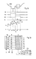
- the carry of the adder 12 is not taken into account in the continuous summation. If the maximum binary value range of the register word is exceeded due to the successive, intermittent accumulation of the accumulator register 11, this assumes the value zero plus the overflowed (low-order) value: consequently, a digital oscillator output signal is present at an output 10 ′′ of the digital oscillator 10 (DCO output signal) as a data signal, which - as can be seen from line 4 of FIG. 2a representing the DCO output signal - has a sawtooth-shaped value profile over time.
- DCO output signal digital oscillator 10
- the successive accumulation of the register word of the accumulator register 11 by the value at the input 10 ' causes the value of the DCO output signal to increase gradually from the value zero to the positive maximum value of the decimal value range during the first half of the digital oscillator period T, in the first cycle of the second half of the digital oscillator period T from the decimal positive maximum value to decimal negative minimum value d it jumps value range and then gradually approaches the initial value zero during the further clock cycles of the second half of the digital oscillator period T.
- This sawtooth-shaped DCO output signal of the digital oscillator 10 represents the phase response of the digital oscillator, with exactly one phase value being assigned to each value of the register word of the accumulator register 11.
- the realization of the digital oscillator 10 as a periodically overflowing accumulator has the effect, in a particularly advantageous manner, that a linear assignment between the amplitude of the DCO output signal and the digital oscillator phase is achieved over the full angular range of 360.
- the DCO output signal is fed to a third input 100 '"of the processor device 100, which has the functional units mentioned below.
- the processing operations of the digital DCO output signal to be carried out in the individual functional units are carried out by a program-controlled microcomputer are executed:
- the above-mentioned functional units thus represent the individual sections of a flow chart of a corresponding computer program.
- a control unit 20 of the processor device 100 is used to control the adjustment of the period duration T of the digital oscillator to be carried out by the processor device 100 to a nominal period duration, which is determined by the period of time that elapses between two synchronizing pulses S1 and S2 that occur periodically.
- the phase adjustment is initiated by the synchronization pulse S1, which is separated from the luminance signal BAS by the pulse separation stage 2 and is passed to the control unit 20 via the first input 100 'of the processor device 100.
- the synchronization pulse S1 triggers the control unit 20, which then stores the current value of the DCO output signal. This value represents the actual phase of the digital oscillator 10 at this trigger time.
- phase comparator unit 30 calculates a phase difference signal from the difference between the actual phase and the target phase, which signal is fed to a first adder unit 40.
- the output signal of the microprocessor of the pulse separation stage 2 is also present at the adder unit 40.
- the phase difference signal having a temporal accuracy of one clock is added to the output signal of the pulse isolating stage 2, which is accurate to a fraction of the clock, in the first adder unit 40.
- the resulting phase difference signal accordingly achieves a temporal resolution of the phase offset of the digital oscillator 10 which is accurate to a fraction of the clock.
- the phase difference signal modified in this way is passed to a loop filter unit 50.
- This has the task of influencing the dynamic properties of the phase control loop in a manner known to the person skilled in the art.
- the filtered phase difference signal is fed to a second adder 60, to which a frequency word f is applied.
- the value of this frequency word f is determined as a function of the predetermined clock of the clock generator 13 and the word length N of the register word of the accumulator register 11 in such a way that the digital oscillator 10 accumulates the register word of the accumulator register 11 by the frequency word f in when the clock word is successively accumulated the nominal period overflows.
- the control word st of the digital oscillator 10 is formed by the addition of the frequency word f and the filtered phase difference signal.
- the value of the control word st represents the instantaneous period of the digital oscillator 10.
- the current control word st formed in the processor device 100 is then fed to the input 10 ′ of the digital oscillator 10.
- the register word of the accumulator register 11 is then successively increased by the current control word during the period determined by the line Z1 (see FIG. 2b) in time with the clock generator 13, as a result of which the frequency or the period duration T of the digital oscillator is approximated 10 to the nominal frequency or nominal period duration predetermined by the synchronization pulses S1-S6.
- the next phase adjustment between the actual phase of the digital oscillator 10 and the predetermined target phase only takes place when the digital phase control loop 1 is triggered by the synchronization pulse S2 occurring at the beginning of line Z2.
- This new phase adjustment then takes place as described above.
- the digital phase control loop 1 therefore carries out the phase adjustment in a first control cycle, which is predetermined by the synchronizing pulses S1, S2 and S3 that occur periodically.
- Such a phase adjustment leads then to the fact that the period T of the digital oscillator 10 is locked in phase lock to the nominal period after a few cycles of the first control cycle.
- the line-periodic synchronization pulse S3 is followed by a non-line-periodic synchronization pulse S4 which is 180 °, i. occurs offset by half a line.
- this non-line-periodic synchronization pulse S4 leads to the fact that the latching of the digital oscillator 10 is disturbed to the nominal period duration, since in these the phase adjustment process occurs through all those reaching the digital phase control loop - also through the non- line periodic - synchronization pulses is triggered.
- phase adjustment between the actual phase and the desired phase is carried out in a second control cycle, which allows the non-line-periodic synchronization pulse S4 to be carried out in such a way Phase control process to include that the detent of the digital oscillator 10 is not disturbed to the nominal period.
- the processor device 100 generates a signal sequence of half the line period duration from the DCO output signal, the period duration TD of which is exactly half the period duration T of the DCO output signal. This signal sequence of half the line period is then used to determine the phase difference.
- the nominal period duration specified by the chronological sequence of the synchronizing pulses S1-S3 occurring in the line period is passed to the second control cycle specified by the line-period synchronizing pulses S1-S3 and the non-line-periodic synchronizing pulse S4 becomes.
- the signal sequence of half the line period is used in order to compare the actual phase of the digital oscillator 10 at the trigger point in time, that is to say when one of the synchronization pulses S1-S3 or S4 occurs, with the desired value specified by the phase word p Phase at this time to determine the phase offset of the digital oscillator, ie to calculate the phase difference signal.
- the phase adjustment carried out in the second control cycle not only ensures that the half-line offset of the non-line-period synchronizing pulse S4 compared to the line-periodically occurring synchronization pulses S1-S3 does not disturb the digital phase control loop 1.
- This operating mode is characterized in that the non-line-period synchronizing pulse S4 is recognized by the phase measurement circuit of the digital oscillator 10.
- Another advantage of the digital phase control loop 1 is that the phase adjustment can now take place twice per line. A particularly rapid transient response of the digital phase control loop 1 is thereby achieved.
- the phase difference between the actual phase and the target phase is measured linearly over half a line - over 180, i.e. with the locked DPLL, the phase measurement is considered at twice the line frequency. Since the phase offset of the digital oscillator 10 is evaluated with half a line period, the digital phase control loop 1 operates in a particularly advantageous manner with two different phases (0 and 1800).
- the signal sequence of half the line period is generated by the control unit 20 from the DCO output signal of the digital oscillator 10 in a particularly simple manner in that it does not consider the signed most significant bit N of the DCO output signal.
- the remaining bits N-1, N-2, ... 1 of the DCO output signal then form the signal sequence of half the line period.
- Their N-1 bits are regarded as the VB representation of a decimal number, which results in the sawtooth-shaped temporal course of the signal sequence of half the line period duration shown by line 8 in FIG. 2a. It is important that this type of generation of the signal sequence of half the line period duration provides its rigid coupling with the DCO output signal.
- Bit N of the DCO output signal is fed as a DPLL output signal to an output of the digital phase control loop 1.
- the time course of the DPLL output signal is represented by line 5 in FIG. 2a. It can be seen that the DPLL output signal in this case has the waveform of a line-frequency square-wave signal. However, it is also possible to generate a DPLL output signal which has a higher precision than the above-mentioned signal represented only by bit N of the DCO output signal. In this case, it is then provided that not only bit N of the DCO output signal, but - depending on the desired precision - bits N-1, etc. are fed to output 1 'of digital phase control loop 1.
- the DCO output signal is fed to a correction device 110. This is used to generate an address phase signal from the DCO output signal, which is then also used to control the lines
- Frequent operations of video signal processing can be used if the chronological sequence of the line-periodic synchronization pulses S1-S3 and S5, S6 is interrupted by a synchronization line S4 occurring non-line-periodically or is shifted by half a line.
- Ki One-bit control signal
- This coupling is effected by means of the digital oscillator 10, the N-digit output signal of which can be defined in binary representation of the respective time stamp of a line by a corresponding numerical value.
- the time stamp t1 thus corresponds to the numerical value N1
- the time stamp t2 corresponds to the numerical value N2 etc.
- the functioning of the key signal generation Ki is shown schematically in FIG. 2d and FIG. 2e for the purpose of clarification using a simple example with three partially overlapping time windows W1, W2, W3 and a single key signal K4.
- the first line shows the signal curve of a color television signal FBAS in the area of the line flyback interval.
- the next three lines each show the temporal position of the first, second and third time window W1, W2, W3.
- the fifth line shows the temporal position of the key signal K4, which only lasts one sampling period.
- the line-periodic DCO output signal is represented by the oblique line 6 shown below, cf. also Fig. 2c.
- each memory cell contains the respectively valid entries of the key signals K1 to K4.
- the programmed numerical value Ni represents the next address word NA in which the combination of the key signals K1 to K4 is to be changed.
- a shift clock g is generated for a cyclic shift register 190, the revolving "1" of which serves as a pointer for the successive memory addresses of the memory 200, cf. 1.
- the three time windows W1, W2, W3 are generated by means of the key entries K1 to K3 which have been read out and a memory circuit 210, 211, 212.
- the individual key signal K4 is used directly as a control signal of the three time window signals are required because the key signals K1 to K4 only have the duration of a single sampling period.
- the comparator 180 is supplied with the address phase signal generated in the correction device 110 from the DCO output signal of the digital oscillator 10. As can be seen from the comparison of the DCO output signal of FIG. 2a represented by line 4 and the address phase signal of FIG. 2c represented by line 6, the latter is identical to the DCO output signal during the period given by lines Z1 and Z2 : The DCO output signal and the address phase signal have identical phase values, which ensures the synchronism of the video signal processing with the time profile of the luminance signal BAS.
- the address phase of the address phase signal must be corrected in order in this case to ensure the synchronism of the line-frequency operations of the video signal processing with the luminance signal BAS.
- the correction device 110 must shift the address phase of the address phase signal by 180 °, that is to say by a period TD of the signal sequence of half the line period.
- the correction device 110 has two XOR gates 150 and 160.
- the most significant bit N of the DCO output signal 10 is applied to a first input 151 of the first XOR gate 150.
- the next lower bit N-1 of the DCO output signal is present at a second input 152 of the first XOR gate 150.
- An output 153 of the first XOR gate 151 is connected to a first input 161 of the second XOR gate 160.
- the most significant bit N of the digital DCO output signal is present at a second input 162 of the second XOR gate 160.
- the DCO output signal and the signal sequence of half the line period duration differ in the case of a non-line-period synchronization pulse S4 phase values. Due to the rigid coupling of the signal sequence of half the line period with the DCO output signal, this difference is always 180 ° at this time. This meant that in the case of a non-line-period synchronizing pulse S4, the bit N and the bit N-1 of the DCO output signal are different, since the signal sequence of half the line period duration is determined by the bits N-1, N-2, ..., 1 of the bits N, N-1, ..., 1 specified DCO output signal is generated.
- Correction device 110 makes it particularly easy to detect a non-line-period synchronization pulse S4 by the non-equivalent assignment of bit N and bit N-1 of the DCO output signal and then to correct the address phase signal by inverting bit N.
Landscapes
- Engineering & Computer Science (AREA)
- Multimedia (AREA)
- Signal Processing (AREA)
- Stabilization Of Oscillater, Synchronisation, Frequency Synthesizers (AREA)
- Synchronizing For Television (AREA)
Priority Applications (5)
| Application Number | Priority Date | Filing Date | Title |
|---|---|---|---|
| DE59010510T DE59010510D1 (de) | 1990-06-30 | 1990-06-30 | Digitale Phasenregelungsschleife |
| EP90112531A EP0464230B1 (fr) | 1990-06-30 | 1990-06-30 | Boucle d'asservissement de phase numérique |
| US07/718,740 US5181115A (en) | 1990-06-30 | 1991-06-21 | Digital phase-locked loop |
| JP91156539A JPH04270570A (ja) | 1990-06-30 | 1991-06-27 | デジタル位相同期ループ回路 |
| KR1019910010871A KR0139197B1 (ko) | 1990-06-30 | 1991-06-28 | 디지탈 위상 고정 루프 회로 |
Applications Claiming Priority (1)
| Application Number | Priority Date | Filing Date | Title |
|---|---|---|---|
| EP90112531A EP0464230B1 (fr) | 1990-06-30 | 1990-06-30 | Boucle d'asservissement de phase numérique |
Publications (2)
| Publication Number | Publication Date |
|---|---|
| EP0464230A1 true EP0464230A1 (fr) | 1992-01-08 |
| EP0464230B1 EP0464230B1 (fr) | 1996-09-18 |
Family
ID=8204160
Family Applications (1)
| Application Number | Title | Priority Date | Filing Date |
|---|---|---|---|
| EP90112531A Expired - Lifetime EP0464230B1 (fr) | 1990-06-30 | 1990-06-30 | Boucle d'asservissement de phase numérique |
Country Status (5)
| Country | Link |
|---|---|
| US (1) | US5181115A (fr) |
| EP (1) | EP0464230B1 (fr) |
| JP (1) | JPH04270570A (fr) |
| KR (1) | KR0139197B1 (fr) |
| DE (1) | DE59010510D1 (fr) |
Families Citing this family (16)
| Publication number | Priority date | Publication date | Assignee | Title |
|---|---|---|---|---|
| DE4102993A1 (de) * | 1991-02-01 | 1992-08-06 | Philips Patentverwaltung | Schaltungsanordnung zur zeitbasis-transformation eines digitalen bildsignals |
| JPH0591522A (ja) * | 1991-09-30 | 1993-04-09 | Toshiba Corp | デイジタル発振器及びこれを用いた色副搬送波再生回路 |
| GB2268656B (en) * | 1992-07-03 | 1995-10-18 | British Broadcasting Corp | Synchronising signal separator |
| US5517685A (en) * | 1993-04-27 | 1996-05-14 | Matsushita Electric Industrial Co., Ltd. | PLL circuit having a multiloop, and FM receiving method and apparatus able to utilize the same |
| US5418573A (en) * | 1993-07-22 | 1995-05-23 | Philips Electronics North America Corporation | Apparatus and method for producing periodic synchronization references forming a synchronization signal |
| US5717469A (en) * | 1994-06-30 | 1998-02-10 | Agfa-Gevaert N.V. | Video frame grabber comprising analog video signals analysis system |
| US6404247B1 (en) | 1995-11-13 | 2002-06-11 | Industrial Technology Research Institute | All digital phase-locked loop |
| JPH1027435A (ja) * | 1996-07-15 | 1998-01-27 | Sony Corp | 再生装置および方法 |
| JP2001513306A (ja) * | 1997-12-22 | 2001-08-28 | コーニンクレッカ フィリップス エレクトロニクス エヌ ヴィ | 時間離散pll回路 |
| CN1135839C (zh) | 1997-12-22 | 2004-01-21 | 皇家菲利浦电子有限公司 | 输出时基校正器、校正方法及具有该校正器的显示设备 |
| US6389548B1 (en) * | 1999-04-12 | 2002-05-14 | Liam Bowles | Pulse run-length measurement for HF data signal by dividing accumulated phase difference between first and second zero-crossings by single-cycle range using multiple cycle range sawtooth waveform |
| DE10026739B4 (de) * | 2000-05-30 | 2006-10-19 | Micronas Gmbh | Verfahren und Vorrichtung zur Phasenkorrektur eines vertikal verzerrten digitalen Bilds |
| US7483508B2 (en) * | 2001-11-27 | 2009-01-27 | Texas Instruments Incorporated | All-digital frequency synthesis with non-linear differential term for handling frequency perturbations |
| FR2854751B1 (fr) * | 2003-05-07 | 2005-07-22 | St Microelectronics Sa | Circuit de recuperation d'horloge |
| US7502953B2 (en) * | 2006-01-05 | 2009-03-10 | International Business Machines Corporation | Dynamically adding additional masters onto multi-mastered IIC buses with tunable performance |
| JP4253740B2 (ja) * | 2006-11-06 | 2009-04-15 | Okiセミコンダクタ株式会社 | 同期信号分離装置 |
Citations (5)
| Publication number | Priority date | Publication date | Assignee | Title |
|---|---|---|---|---|
| US4330791A (en) * | 1978-07-10 | 1982-05-18 | Victor Company Of Japan, Ltd. | System for processing television video signals reproduced from a recording medium in special reproduction mode into signals for performing normal interlacing |
| EP0062541A1 (fr) * | 1981-04-07 | 1982-10-13 | Honeywell Information Systems Inc. | Oscillateurs verouillés en phase |
| US4689664A (en) * | 1984-09-03 | 1987-08-25 | U.S. Philips Corporation | Circuit arrangement for deriving digital color signals from an analog television signal |
| EP0239413A2 (fr) * | 1986-03-28 | 1987-09-30 | RCA Thomson Licensing Corporation | Circuit de stabilisation de boucle à verrouillage de phase |
| EP0239412A2 (fr) * | 1986-03-28 | 1987-09-30 | RCA Thomson Licensing Corporation | Circuit de stabilisation pour boucle d'asservissement de phase numérique |
Family Cites Families (4)
| Publication number | Priority date | Publication date | Assignee | Title |
|---|---|---|---|---|
| US4802009A (en) * | 1987-07-13 | 1989-01-31 | Rca Licensing Corporation | Digitally controlled phase locked loop system |
| US4791488A (en) * | 1987-08-12 | 1988-12-13 | Rca Licensing Corporation | Line-locked clock signal generation system |
| DE3783458D1 (de) * | 1987-10-02 | 1993-02-18 | Itt Ind Gmbh Deutsche | Digitale erzeugung von vertikalsynchron- und halbbild-identifikationssignalen. |
| US4884040A (en) * | 1988-09-26 | 1989-11-28 | Rca Licensing Corporation | Sampled data phase locking system |
-
1990
- 1990-06-30 EP EP90112531A patent/EP0464230B1/fr not_active Expired - Lifetime
- 1990-06-30 DE DE59010510T patent/DE59010510D1/de not_active Expired - Fee Related
-
1991
- 1991-06-21 US US07/718,740 patent/US5181115A/en not_active Expired - Fee Related
- 1991-06-27 JP JP91156539A patent/JPH04270570A/ja active Pending
- 1991-06-28 KR KR1019910010871A patent/KR0139197B1/ko not_active Expired - Fee Related
Patent Citations (5)
| Publication number | Priority date | Publication date | Assignee | Title |
|---|---|---|---|---|
| US4330791A (en) * | 1978-07-10 | 1982-05-18 | Victor Company Of Japan, Ltd. | System for processing television video signals reproduced from a recording medium in special reproduction mode into signals for performing normal interlacing |
| EP0062541A1 (fr) * | 1981-04-07 | 1982-10-13 | Honeywell Information Systems Inc. | Oscillateurs verouillés en phase |
| US4689664A (en) * | 1984-09-03 | 1987-08-25 | U.S. Philips Corporation | Circuit arrangement for deriving digital color signals from an analog television signal |
| EP0239413A2 (fr) * | 1986-03-28 | 1987-09-30 | RCA Thomson Licensing Corporation | Circuit de stabilisation de boucle à verrouillage de phase |
| EP0239412A2 (fr) * | 1986-03-28 | 1987-09-30 | RCA Thomson Licensing Corporation | Circuit de stabilisation pour boucle d'asservissement de phase numérique |
Also Published As
| Publication number | Publication date |
|---|---|
| JPH04270570A (ja) | 1992-09-25 |
| US5181115A (en) | 1993-01-19 |
| DE59010510D1 (de) | 1996-10-24 |
| KR920001935A (ko) | 1992-01-30 |
| EP0464230B1 (fr) | 1996-09-18 |
| KR0139197B1 (ko) | 1998-06-15 |
Similar Documents
| Publication | Publication Date | Title |
|---|---|---|
| EP0464230B1 (fr) | Boucle d'asservissement de phase numérique | |
| DE3841512C2 (fr) | ||
| EP0177076B1 (fr) | Circuit de conversion d'un signal de télévision analogique en signaux de couleurs numériques | |
| DE2720747B2 (de) | Taktimpuls-Regenerator | |
| DE3236311C2 (fr) | ||
| DE2435782C3 (de) | Sägezahn-Funktionsgenerator | |
| DE69123473T2 (de) | Schaltungsanordnung zum Ableiten eines Bitsynchronisierungssignals mittels Rahmensynchronisation | |
| DE3333019A1 (de) | Synchronisierschaltung | |
| DE2711952C2 (de) | Phasenregelschaltung für einen wechselnder Belastung ausgesetzten Antriebsmotor, insbesondere eines Videomagnetbandgeräts | |
| DE4011241B4 (de) | Digitale Fernsehsignalverarbeitungsschaltung mit orthogonalem Ausgangstakt | |
| EP1216509B1 (fr) | Circuit de production d'un signal de synchronisation synchronise en frequence avec des signaux de synchronisation de reference | |
| DE68925320T2 (de) | Bezugssignal-Erzeugungskreis für Phasen-Servosteuerung | |
| DE69215945T2 (de) | Synchronisationstaktgenerator | |
| DE69026284T2 (de) | Digitale Phasenregelschleife | |
| DE69409903T2 (de) | Digitaler Phasenkomparator | |
| WO1985002731A1 (fr) | Circuit de reglage de phase | |
| EP0630129A2 (fr) | Méthode de génération d'un signal d'horloge synchronisé avec un circuit d'oscillateur réglable | |
| DE1809810A1 (de) | Verfahren und Geraet zum Bestimmen der Periodendaueraenderung einer Schwingung | |
| DE69832239T2 (de) | Phasenregelkreisschaltung | |
| DE69800528T2 (de) | Videosignalsynchronisierungsgerät | |
| WO2008116517A1 (fr) | Procédé permettant de générer une fréquence d'horloge | |
| DE69015560T2 (de) | Schaltungsanordnung in einer Bildwiedergabeanordnung mit einer Videosignalverarbeitungsschaltung und einer Zeilensynchronschaltung. | |
| DE2613930C3 (de) | Digitaler Phasenregelkreis | |
| DE3604965C1 (de) | Verfahren und Schaltungsanordnung zum Synchronisieren eines insbesondere einer Vermittlungseinrichtung zugehoerigen spannungsgesteuerten Oszillators | |
| DE102014109471B4 (de) | Takt-Wiederherstellung mit Frequenzsynchronisation |
Legal Events
| Date | Code | Title | Description |
|---|---|---|---|
| PUAI | Public reference made under article 153(3) epc to a published international application that has entered the european phase |
Free format text: ORIGINAL CODE: 0009012 |
|
| AK | Designated contracting states |
Kind code of ref document: A1 Designated state(s): DE FR GB IT NL |
|
| 17P | Request for examination filed |
Effective date: 19920620 |
|
| 17Q | First examination report despatched |
Effective date: 19940801 |
|
| GRAH | Despatch of communication of intention to grant a patent |
Free format text: ORIGINAL CODE: EPIDOS IGRA |
|
| GRAH | Despatch of communication of intention to grant a patent |
Free format text: ORIGINAL CODE: EPIDOS IGRA |
|
| GRAA | (expected) grant |
Free format text: ORIGINAL CODE: 0009210 |
|
| AK | Designated contracting states |
Kind code of ref document: B1 Designated state(s): DE FR GB IT NL |
|
| ITF | It: translation for a ep patent filed | ||
| REF | Corresponds to: |
Ref document number: 59010510 Country of ref document: DE Date of ref document: 19961024 |
|
| GBT | Gb: translation of ep patent filed (gb section 77(6)(a)/1977) |
Effective date: 19961010 |
|
| ET | Fr: translation filed |
Free format text: CORRECTIONS |
|
| PLBE | No opposition filed within time limit |
Free format text: ORIGINAL CODE: 0009261 |
|
| STAA | Information on the status of an ep patent application or granted ep patent |
Free format text: STATUS: NO OPPOSITION FILED WITHIN TIME LIMIT |
|
| 26N | No opposition filed | ||
| PGFP | Annual fee paid to national office [announced via postgrant information from national office to epo] |
Ref country code: FR Payment date: 19980520 Year of fee payment: 9 |
|
| PGFP | Annual fee paid to national office [announced via postgrant information from national office to epo] |
Ref country code: GB Payment date: 19980526 Year of fee payment: 9 |
|
| PGFP | Annual fee paid to national office [announced via postgrant information from national office to epo] |
Ref country code: NL Payment date: 19980527 Year of fee payment: 9 |
|
| PGFP | Annual fee paid to national office [announced via postgrant information from national office to epo] |
Ref country code: DE Payment date: 19980626 Year of fee payment: 9 |
|
| PG25 | Lapsed in a contracting state [announced via postgrant information from national office to epo] |
Ref country code: GB Free format text: LAPSE BECAUSE OF NON-PAYMENT OF DUE FEES Effective date: 19990630 Ref country code: FR Free format text: THE PATENT HAS BEEN ANNULLED BY A DECISION OF A NATIONAL AUTHORITY Effective date: 19990630 |
|
| PG25 | Lapsed in a contracting state [announced via postgrant information from national office to epo] |
Ref country code: NL Free format text: LAPSE BECAUSE OF NON-PAYMENT OF DUE FEES Effective date: 20000101 |
|
| GBPC | Gb: european patent ceased through non-payment of renewal fee |
Effective date: 19990630 |
|
| NLV4 | Nl: lapsed or anulled due to non-payment of the annual fee |
Effective date: 20000101 |
|
| PG25 | Lapsed in a contracting state [announced via postgrant information from national office to epo] |
Ref country code: DE Free format text: LAPSE BECAUSE OF NON-PAYMENT OF DUE FEES Effective date: 20000503 |
|
| REG | Reference to a national code |
Ref country code: FR Ref legal event code: ST |
|
| PG25 | Lapsed in a contracting state [announced via postgrant information from national office to epo] |
Ref country code: IT Free format text: LAPSE BECAUSE OF NON-PAYMENT OF DUE FEES;WARNING: LAPSES OF ITALIAN PATENTS WITH EFFECTIVE DATE BEFORE 2007 MAY HAVE OCCURRED AT ANY TIME BEFORE 2007. THE CORRECT EFFECTIVE DATE MAY BE DIFFERENT FROM THE ONE RECORDED. Effective date: 20050630 |