EP0464548A2 - Halbleiterspeicheranordnung - Google Patents
Halbleiterspeicheranordnung Download PDFInfo
- Publication number
- EP0464548A2 EP0464548A2 EP91110358A EP91110358A EP0464548A2 EP 0464548 A2 EP0464548 A2 EP 0464548A2 EP 91110358 A EP91110358 A EP 91110358A EP 91110358 A EP91110358 A EP 91110358A EP 0464548 A2 EP0464548 A2 EP 0464548A2
- Authority
- EP
- European Patent Office
- Prior art keywords
- line
- bit line
- memory device
- semiconductor memory
- sense amplifier
- Prior art date
- Legal status (The legal status is an assumption and is not a legal conclusion. Google has not performed a legal analysis and makes no representation as to the accuracy of the status listed.)
- Granted
Links
Images


Classifications
-
- G—PHYSICS
- G11—INFORMATION STORAGE
- G11C—STATIC STORES
- G11C11/00—Digital stores characterised by the use of particular electric or magnetic storage elements; Storage elements therefor
- G11C11/21—Digital stores characterised by the use of particular electric or magnetic storage elements; Storage elements therefor using electric elements
- G11C11/34—Digital stores characterised by the use of particular electric or magnetic storage elements; Storage elements therefor using electric elements using semiconductor devices
- G11C11/40—Digital stores characterised by the use of particular electric or magnetic storage elements; Storage elements therefor using electric elements using semiconductor devices using transistors
- G11C11/401—Digital stores characterised by the use of particular electric or magnetic storage elements; Storage elements therefor using electric elements using semiconductor devices using transistors forming cells needing refreshing or charge regeneration, i.e. dynamic cells
- G11C11/4063—Auxiliary circuits, e.g. for addressing, decoding, driving, writing, sensing or timing
- G11C11/407—Auxiliary circuits, e.g. for addressing, decoding, driving, writing, sensing or timing for memory cells of the field-effect type
- G11C11/4074—Power supply or voltage generation circuits, e.g. bias voltage generators, substrate voltage generators, back-up power, power control circuits
-
- G—PHYSICS
- G11—INFORMATION STORAGE
- G11C—STATIC STORES
- G11C11/00—Digital stores characterised by the use of particular electric or magnetic storage elements; Storage elements therefor
- G11C11/21—Digital stores characterised by the use of particular electric or magnetic storage elements; Storage elements therefor using electric elements
- G11C11/34—Digital stores characterised by the use of particular electric or magnetic storage elements; Storage elements therefor using electric elements using semiconductor devices
- G11C11/40—Digital stores characterised by the use of particular electric or magnetic storage elements; Storage elements therefor using electric elements using semiconductor devices using transistors
- G11C11/401—Digital stores characterised by the use of particular electric or magnetic storage elements; Storage elements therefor using electric elements using semiconductor devices using transistors forming cells needing refreshing or charge regeneration, i.e. dynamic cells
- G11C11/4063—Auxiliary circuits, e.g. for addressing, decoding, driving, writing, sensing or timing
- G11C11/407—Auxiliary circuits, e.g. for addressing, decoding, driving, writing, sensing or timing for memory cells of the field-effect type
- G11C11/409—Read-write [R-W] circuits
- G11C11/4094—Bit-line management or control circuits
Definitions
- the present invention relates to a circuit arrangement designed to secure a minute signal from a bit line which is input to a sense amplifier in a dynamic semiconductor memory device.
- DRAM dynamic semiconductor memory
- one-bit data is stored as electric charge in a memory cell comprised of one transistor and one capacitor.
- the capacitor where the data is stored is connected with a precharged bit line.
- the potential change of the bit line at this time is amplified by a sense amplifier between the bit line and a reference line in pairs, and transmitted to an output circuit.
- the data is read out from the conventional DRAM described above in a manner as follows.
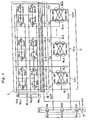
- Fig. 4 is a circuit diagram showing the structure of a memory cell array part and the sense amplifiers SA1, SA2, ..., SA m of the conventional DRAM.
- Each sense amplifier is comprised of a differential amplifier being consisted of a pair of N-type transistors, for example, QN1, QN1', and a pair of P-type transistors, for example, QP1, QP1'.
- Two bit lines BL1, BL1 ⁇ are connected to the sense amplifier SA1 as one pair of inputs.
- Each bit line BLi or BLi ⁇ is connected to each data memory capacitor mCi.1 or mCi.2 which is connected between a MOS transistor Qi.1 or Qi.2 as a transfer gate and a fixed voltage electrode Vcp.
- the MOS transistor as a transfer gate is controlled in response to the selection of a word line among word lines WL1 WL2, ..., WLn.
- a common node SAP of the P-type transistors and a common node SAN of the N-type transistors of the sense amplifier are connected to precharging transistors Qp, QN and an equalizer transistor QEQ, respectively.
- Fig. 5 is a schematic timing chart of the operation and waveforms of the conventional DRAM.
- a clock ⁇ 1 is set at Vcc and the equalizer transistor QEQ is turned on thereby, with a clock ⁇ 2 being set at 0 and a clock ⁇ 3 being set at Vcc, thereby to turn off the precharging transistors QN and QP.
- the common node SAP (referred to as SAP hereinafter) and the common node SAN (referred to as SAN hereinafter) are set at 1/2Vcc, and the transistors QN1, QN1', ..., QNm and QNm' for driving the sense amplifier are kept in the off state.
- bit lines are set at 1/2Vcc by means of equalizer transistors and precharging transistors (not shown in Fig. 4).
- the clock ⁇ 1 is turned to 0 thereby turning off the equalizer transistor QEQ, to release the connection between SAP and SAN.
- the level of a word line corresponding to the input address is raised at a next timing.
- capacitors connected to the word line are connected with the respective bit lines and the level of each bit line is changed in response to each charging state corresponding to the data memorized in each capacitor.
- SAN is set at 0 by turning the clock ⁇ 2 to Vcc
- SAP is set at Vcc by turning the clock ⁇ 3 to 0.
- each sense amplifier detects the above level change, and amplifies the level of the corresponding bit line to Vcc or 0. For example, when the potential of word line WL1 is raised, as indicated in (b) of Fig. 5, the transistor Q1.1 is turned on thereby and, accordingly, the capacitor is connected to the bit line BL1. If it is in the not charge state, a negative level change ⁇ V is given to the bit line BL1 as shown in (g) of Fig. 5.
- bit line BL1 is moved to 0 due to a differential amplification between ⁇ V and 1/2Vcc of the corresponding bit line BL1 ⁇ which is not changed by the word line WL2, whereas the bit line BL1 ⁇ is moved to Vcc.
- the same change is brought about in the other capacitors mc2.1, ..., mcm.1, connected to the word line WL1.
- the charging state of each capacitor corresponding to the word line is read out as the level change of each bit line.
- the word line is finally turned off after a predetermined reset period. The level of each bit line is thus held in the respective capacitor.
- QN2' allows a current to flow since it starts with the potential difference ⁇ V from the beginning, and BL2 ⁇ alike starts to fall. Meanwhile, although QN2 starts from the potential difference 0, it is turned off due to the level fall of the gate by BL2, and BL2 is maintained at 1/2Vcc+ ⁇ V .
- QN1' starts from a disadvantageous potential difference, i.e., the gate is ⁇ V lower than the source, the change of the QN' level is behind the fall of the SAN level, and BL1 ⁇ remains at 1/2Vcc until then.
- QN1 is, starting from the potential difference 0, later to fall than SAN.
- the BL1 level is maintained at 1/2Vcc- ⁇ V until then.
- a current equivalent to the reading current of QN2' is produced at many capacitors. Therefore, when the impedance of Vss line is high, as shown in (f) of Fig. 5, ⁇ Vss voltage is generated in Vss line and the SAN level is raised as indicated in (e) of Fig. 5. As a result, QN1 and QN1' are hindered from being changed in level, delayed until SAN is recovered to Vss after the capacitors are completely discharged.
- Waveforms in Fig. 5 represent the result of the delay in total.
- the delay in the level change of the bit lines as noted hereinabove necessitates a time for the sense amplifier to obtain the driving margin, making it hard to achieve high-speed access.
- the present invention has been devised to solve the above-described disadvantages inherent in the prior art, and has for its essential object to provide a DRAM capable of securing a margin for a sense amplifier and realizing high-speed access with quick level change of a bit line.
- a compensation capacitor is inserted between an input terminal of each bit line and a Vss line of sense amplifiers of a DRAM.
- the compensation capacitor changes the level of a pair of bit lines in compliance with the change of the Vss line, so that the change in the source level of N type transistors of the sense amplifier can be negated, thereby reducing the operation delay.
- Fig. 1 is a circuit diagram showing the structure of the DRAM according to a preferred embodiment of the present invention which is essentially comprised of a memory cell array 1 and a sense amplifier array 2.
- a data memory capacitor mci.j-1 or mci.j as a charge-storage memory is connected at one end thereof via a MOS transistor Qi.j-1 or Qi.j as a transfer gate which is controlled by(j-1)-th word line WLj-1 or j-th word line WLj.
- the other end of the capacitor is connected to a fixed electrode Vcp for charging the same.
- a common node SAP of the P-type transistors and a common node SAN of the N-type transistors of each sense amplifier are connected with respective driving transistors QP,QN and a equalizer transistor QEQ.
- the DRAM according to the present invention provides with coupling capacitors C1, C'1, ..., Cm and C'm each of which is connected between a ground potential line Vss as a source electrode of the driving transistor QN and each bit line.
- the i-th coupling capacitor Ci or C'i is connected between Vss and the i-th bit line BLi or BLi ⁇ .
- the semiconductor memory device of the present invention is different from the conventional one in that the above-described capacitors C1, C1', ..., Cm, Cm' are provided therein.
- both transistors Qp and Qn are in the off state, and both SAN and SAP are kept at 1/2Vcc by the equalizer transistor QEQ.
- the sense amplifiers SA1, to SAm connected to these transistors and each bit line are held at 1/2Vcc similar to the conventional device.
- the DRAM becomes a drivable state
- the potential of clock ⁇ 1 is fallen to "L" level and, thereby, the equalizer transistor QEQ is turned off.
- Each bit line is turned off by turning off corresponding equalizer transistor and precharging transistor (not shown in Fig. 1).
- MOS transistors Q1.1, Q2.1, ..., Qm.1 connected to the word line WL1 are turned on and, thereby, the data memory capacitors mc1.1,mc2.1, ..., mcm.1 connected to the respective MOS transistors Q1.1, Q2.1, ..., Qm.1 are connected to the bit lines BL1, BL2, ..., BLm, respectively.
- the potential difference is brought about on each bit line corresponding to the data memorized in the data memory capacitors.
- the driving transistor QN is turned on by the clock ⁇ 2 in order to amplify this potential by each sense amplifier SA1, or SA2 with reference to 1/2 Vcc level of the reference bit line BL1 ⁇ or BL2 ⁇ .
- Such potential changes are caused in each bit line.
- read out currents flow into Vss line from each bit line via the N-type transistors of each sense amplifier and due to the impedance resulting from the wiring for Vss(SA) within the DRAM, the level of Vss is raised by ⁇ Vss, as shown in (f) of Fig. 2.
- each level of BL1, BL1 ⁇ , BL2 and BL2 is raises by an equal amount, as shown in waveforms (g) and (h) of Fig. 2.
- potential difference between BL1 and BL1 ⁇ and/or BL2 and BL2 ⁇ is kept unchanged in spite of the rise of the potential of Vss. Therefore, the potential difference between the pair of bit lines BL1 and BL1 ⁇ is amplified by the sense amplifier SA1 without delay in comparison with that between the pair of bit lines BL2 and BL2 ⁇ , that is, both potential differences between BL1 and BL1 ⁇ and between BL2 and BL2 ⁇ are amplified by respective sense amplifiers simultaneously.
- the precharging transistor QP is turned on by a clock ⁇ 3 and, thereby, the bit lines at "High” side are raised upto Vcc and those at “Low” side are fallen down to zero.
- the word line WL1 is turned off and all MOS transistors connected thereto. Thus, each data is stored in each data memory capacitor.
- compensation capacitors can be connected between SAN line and each bit line, as indicated by dotted lines in Fig. 2.
- each bit line is connected to Vss line by a capacitor, thereby removing the influences of the potential change generated in Vss line by the reading currents and also the operation delay of the bit line, while achieving high-speed access.
- each compensation capacitor can be obtained by forming an aluminum pattern line 10 to be connected to Vss line on an inter-layer insulation film 11 covering bit lines.
- This aluminum pattern line 10 can be easily formed together with other aluminum word line electrodes 12 using the photolithograpic technic.
- the DRAM according to the preferred embodiment of the present invention is different from the conventional DRAM only in that the aluminum electrode 10 is provided for forming a compensation capacitor Cn between it and the bit line BLn as indicated in Fig. 3.
- LOCOS denotes an isolation layer formed by local oxidization method
- n+ or n ⁇ denotes n-type doped domain
- PS denotes a first poly-silicon layer used for forming a fixed electrode Vcp
- PP denotes a second poly-silicon layer forming a word line as a gate of a switching transistor
- PB denotes a laminated layer of metal silicate and poly-silicon
- AL denotes an aluminum electrode line.
- the semiconductor memory device provided with memory means for storing bit information by the storing state of electric charges input/output due to the potential change between a word line and a bit line
- a sense amplifier connected to the bit line of the memory means to input/output the electric charges and, power source means for feeding the driving source for the sense amplifier from a source line through control of clocks
- the bit line is connected to the flow-in side of the reading current of the source line by a compensation capacitor. Therefore, it becomes possible to remove the influences of the transitional potential change in the source line by the reading current and to remove the changing delay in the reading potential of the bit line, thereby achieving high-speed access.
Landscapes
- Engineering & Computer Science (AREA)
- Microelectronics & Electronic Packaging (AREA)
- Computer Hardware Design (AREA)
- Dram (AREA)
Applications Claiming Priority (2)
| Application Number | Priority Date | Filing Date | Title |
|---|---|---|---|
| JP2167199A JPH0460984A (ja) | 1990-06-25 | 1990-06-25 | 半導体記憶装置 |
| JP167199/90 | 1990-06-25 |
Publications (3)
| Publication Number | Publication Date |
|---|---|
| EP0464548A2 true EP0464548A2 (de) | 1992-01-08 |
| EP0464548A3 EP0464548A3 (en) | 1993-08-11 |
| EP0464548B1 EP0464548B1 (de) | 1996-11-27 |
Family
ID=15845264
Family Applications (1)
| Application Number | Title | Priority Date | Filing Date |
|---|---|---|---|
| EP91110358A Expired - Lifetime EP0464548B1 (de) | 1990-06-25 | 1991-06-24 | Halbleiterspeicheranordnung |
Country Status (4)
| Country | Link |
|---|---|
| US (1) | US5406512A (de) |
| EP (1) | EP0464548B1 (de) |
| JP (1) | JPH0460984A (de) |
| DE (1) | DE69123294T2 (de) |
Cited By (2)
| Publication number | Priority date | Publication date | Assignee | Title |
|---|---|---|---|---|
| EP0627741A3 (de) * | 1993-04-09 | 1996-06-12 | Matsushita Electric Industrial Co Ltd | Halbleiterspeicheranordnung. |
| DE19735136C1 (de) * | 1997-08-13 | 1998-10-01 | Siemens Ag | Schaltungsanordnung für die Bewertung des Dateninhalts von Speicherzellen |
Families Citing this family (10)
| Publication number | Priority date | Publication date | Assignee | Title |
|---|---|---|---|---|
| US5452244A (en) * | 1994-08-10 | 1995-09-19 | Cirrus Logic, Inc. | Electronic memory and methods for making and using the same |
| JP3400181B2 (ja) * | 1995-04-25 | 2003-04-28 | ローム株式会社 | 半導体装置およびその製造方法 |
| US5608249A (en) | 1995-11-16 | 1997-03-04 | Micron Technology, Inc. | Reduced area storage node junction |
| KR100231404B1 (ko) * | 1996-02-22 | 1999-11-15 | 가네꼬 히사시 | 다수의 값을 갖는 소형 반도체 메모리 디바이스 |
| US6124199A (en) * | 1999-04-28 | 2000-09-26 | International Business Machines Corporation | Method for simultaneously forming a storage-capacitor electrode and interconnect |
| US6201272B1 (en) | 1999-04-28 | 2001-03-13 | International Business Machines Corporation | Method for simultaneously forming a storage-capacitor electrode and interconnect |
| US6399975B1 (en) * | 2001-03-07 | 2002-06-04 | Megic Corporation | Wide bit memory using post passivation interconnection scheme |
| WO2003021975A2 (de) * | 2001-08-28 | 2003-03-13 | Siemens Aktiengesellschaft | Baugruppe, rückwand sowie bidirektionaler multiplexer |
| CN1901162B (zh) * | 2005-07-22 | 2011-04-20 | 米辑电子股份有限公司 | 连续电镀制作线路组件的方法及线路组件结构 |
| US8310859B2 (en) | 2008-09-30 | 2012-11-13 | Samsung Electronics Co., Ltd. | Semiconductor memory device having balancing capacitors |
Family Cites Families (6)
| Publication number | Priority date | Publication date | Assignee | Title |
|---|---|---|---|---|
| US4584672A (en) * | 1984-02-22 | 1986-04-22 | Intel Corporation | CMOS dynamic random-access memory with active cycle one half power supply potential bit line precharge |
| JPS60239993A (ja) * | 1984-05-12 | 1985-11-28 | Sharp Corp | ダイナミツク型半導体記憶装置 |
| JPS61276198A (ja) * | 1985-04-26 | 1986-12-06 | アドバンスト・マイクロ・デイバイシズ・インコ−ポレ−テツド | Cmosメモリバイアスシステム |
| JPS63133394A (ja) * | 1986-11-21 | 1988-06-06 | Nec Ic Microcomput Syst Ltd | 半導体記憶装置 |
| JPS63183691A (ja) * | 1987-01-26 | 1988-07-29 | Mitsubishi Electric Corp | 半導体記憶装置 |
| DE68905240T2 (de) * | 1988-06-01 | 1993-07-15 | Nippon Electric Co | Halbleiterspeichereinrichtung mit hochgeschwindigkeits-lesevorrichtung. |
-
1990
- 1990-06-25 JP JP2167199A patent/JPH0460984A/ja active Pending
-
1991
- 1991-06-24 EP EP91110358A patent/EP0464548B1/de not_active Expired - Lifetime
- 1991-06-24 DE DE69123294T patent/DE69123294T2/de not_active Expired - Fee Related
-
1993
- 1993-12-13 US US08/166,158 patent/US5406512A/en not_active Expired - Lifetime
Cited By (2)
| Publication number | Priority date | Publication date | Assignee | Title |
|---|---|---|---|---|
| EP0627741A3 (de) * | 1993-04-09 | 1996-06-12 | Matsushita Electric Industrial Co Ltd | Halbleiterspeicheranordnung. |
| DE19735136C1 (de) * | 1997-08-13 | 1998-10-01 | Siemens Ag | Schaltungsanordnung für die Bewertung des Dateninhalts von Speicherzellen |
Also Published As
| Publication number | Publication date |
|---|---|
| US5406512A (en) | 1995-04-11 |
| EP0464548B1 (de) | 1996-11-27 |
| JPH0460984A (ja) | 1992-02-26 |
| DE69123294D1 (de) | 1997-01-09 |
| EP0464548A3 (en) | 1993-08-11 |
| DE69123294T2 (de) | 1997-05-07 |
Similar Documents
| Publication | Publication Date | Title |
|---|---|---|
| US4855628A (en) | Sense amplifier for high performance dram | |
| EP0474238B1 (de) | Halbleiterspeicherschaltung | |
| US4417329A (en) | Active pull-up circuit | |
| KR900006191B1 (ko) | 반도체 기억장치 | |
| US4616343A (en) | Semiconductor memory device | |
| US6154402A (en) | Semiconductor memory device | |
| EP0464548B1 (de) | Halbleiterspeicheranordnung | |
| US4370737A (en) | Sense amplifier and sensing methods | |
| JP3399787B2 (ja) | 半導体記憶装置 | |
| US4262341A (en) | Memory circuit | |
| EP0073677B1 (de) | MIS Transistorschaltung mit einer Spannungshalteschaltung | |
| EP0398244A2 (de) | Direktzugriffsspeicher vom dynamischen Typ | |
| US4409672A (en) | Dynamic semiconductor memory device | |
| US4387448A (en) | Dynamic semiconductor memory device with decreased clocks | |
| EP0053877A2 (de) | Bitleitungsvorladeschaltung für einen dynamischen Halbleiterspeicher | |
| US5777934A (en) | Semiconductor memory device with variable plate voltage generator | |
| US7663952B2 (en) | Capacitor supported precharging of memory digit lines | |
| US4484312A (en) | Dynamic random access memory device | |
| EP0451000B1 (de) | Halbleiter-Speichereinrichtung mit verbesserter Kontrollfunktion für Datenbusse | |
| US6970390B2 (en) | DRAM memory circuit with sense amplifiers | |
| JPS6212992A (ja) | 半導体記憶装置 | |
| Sheikholeslami | A circuit to remember [Circuit Intuitions] | |
| JP3152751B2 (ja) | 半導体集積回路 | |
| JP2003016783A (ja) | 半導体記憶装置 | |
| GB2250363A (en) | Equalizing semiconductor memory bitlines with PMOS transistor |
Legal Events
| Date | Code | Title | Description |
|---|---|---|---|
| PUAI | Public reference made under article 153(3) epc to a published international application that has entered the european phase |
Free format text: ORIGINAL CODE: 0009012 |
|
| 17P | Request for examination filed |
Effective date: 19910624 |
|
| AK | Designated contracting states |
Kind code of ref document: A2 Designated state(s): DE FR GB NL |
|
| PUAL | Search report despatched |
Free format text: ORIGINAL CODE: 0009013 |
|
| AK | Designated contracting states |
Kind code of ref document: A3 Designated state(s): DE FR GB NL |
|
| GRAG | Despatch of communication of intention to grant |
Free format text: ORIGINAL CODE: EPIDOS AGRA |
|
| 17Q | First examination report despatched |
Effective date: 19960322 |
|
| GRAH | Despatch of communication of intention to grant a patent |
Free format text: ORIGINAL CODE: EPIDOS IGRA |
|
| GRAH | Despatch of communication of intention to grant a patent |
Free format text: ORIGINAL CODE: EPIDOS IGRA |
|
| GRAA | (expected) grant |
Free format text: ORIGINAL CODE: 0009210 |
|
| AK | Designated contracting states |
Kind code of ref document: B1 Designated state(s): DE FR GB NL |
|
| ET | Fr: translation filed | ||
| REF | Corresponds to: |
Ref document number: 69123294 Country of ref document: DE Date of ref document: 19970109 |
|
| PLBE | No opposition filed within time limit |
Free format text: ORIGINAL CODE: 0009261 |
|
| STAA | Information on the status of an ep patent application or granted ep patent |
Free format text: STATUS: NO OPPOSITION FILED WITHIN TIME LIMIT |
|
| 26N | No opposition filed | ||
| PGFP | Annual fee paid to national office [announced via postgrant information from national office to epo] |
Ref country code: FR Payment date: 19980609 Year of fee payment: 8 |
|
| PGFP | Annual fee paid to national office [announced via postgrant information from national office to epo] |
Ref country code: GB Payment date: 19980615 Year of fee payment: 8 |
|
| PGFP | Annual fee paid to national office [announced via postgrant information from national office to epo] |
Ref country code: NL Payment date: 19980629 Year of fee payment: 8 |
|
| PGFP | Annual fee paid to national office [announced via postgrant information from national office to epo] |
Ref country code: DE Payment date: 19980706 Year of fee payment: 8 |
|
| PG25 | Lapsed in a contracting state [announced via postgrant information from national office to epo] |
Ref country code: GB Free format text: LAPSE BECAUSE OF NON-PAYMENT OF DUE FEES Effective date: 19990624 |
|
| PG25 | Lapsed in a contracting state [announced via postgrant information from national office to epo] |
Ref country code: FR Free format text: THE PATENT HAS BEEN ANNULLED BY A DECISION OF A NATIONAL AUTHORITY Effective date: 19990630 |
|
| PG25 | Lapsed in a contracting state [announced via postgrant information from national office to epo] |
Ref country code: NL Free format text: LAPSE BECAUSE OF NON-PAYMENT OF DUE FEES Effective date: 20000101 |
|
| GBPC | Gb: european patent ceased through non-payment of renewal fee |
Effective date: 19990624 |
|
| NLV4 | Nl: lapsed or anulled due to non-payment of the annual fee |
Effective date: 20000101 |
|
| PG25 | Lapsed in a contracting state [announced via postgrant information from national office to epo] |
Ref country code: DE Free format text: LAPSE BECAUSE OF NON-PAYMENT OF DUE FEES Effective date: 20000503 |
|
| REG | Reference to a national code |
Ref country code: FR Ref legal event code: ST |