EP0464556A2 - Appareil de commande d'une source de lumière et système de formation d'images utilisant un tel appareil - Google Patents
Appareil de commande d'une source de lumière et système de formation d'images utilisant un tel appareil Download PDFInfo
- Publication number
- EP0464556A2 EP0464556A2 EP91110371A EP91110371A EP0464556A2 EP 0464556 A2 EP0464556 A2 EP 0464556A2 EP 91110371 A EP91110371 A EP 91110371A EP 91110371 A EP91110371 A EP 91110371A EP 0464556 A2 EP0464556 A2 EP 0464556A2
- Authority
- EP
- European Patent Office
- Prior art keywords
- light
- light source
- polarized
- driving apparatus
- image forming
- Prior art date
- Legal status (The legal status is an assumption and is not a legal conclusion. Google has not performed a legal analysis and makes no representation as to the accuracy of the status listed.)
- Granted
Links
- 238000001514 detection method Methods 0.000 claims abstract description 33
- 239000004065 semiconductor Substances 0.000 claims description 55
- 230000008859 change Effects 0.000 claims description 19
- 238000012937 correction Methods 0.000 claims description 12
- 230000001965 increasing effect Effects 0.000 claims description 12
- 230000000694 effects Effects 0.000 claims description 9
- 230000003287 optical effect Effects 0.000 claims description 8
- 230000004044 response Effects 0.000 claims description 5
- 229910052709 silver Inorganic materials 0.000 claims description 4
- 239000004332 silver Substances 0.000 claims description 4
- -1 silver halide Chemical class 0.000 claims description 4
- 238000012544 monitoring process Methods 0.000 description 27
- 239000010408 film Substances 0.000 description 14
- 230000008033 biological extinction Effects 0.000 description 9
- 238000000034 method Methods 0.000 description 8
- 238000004519 manufacturing process Methods 0.000 description 5
- 230000010355 oscillation Effects 0.000 description 5
- 230000004304 visual acuity Effects 0.000 description 5
- 230000001276 controlling effect Effects 0.000 description 4
- 230000007423 decrease Effects 0.000 description 4
- 230000006872 improvement Effects 0.000 description 4
- 230000009467 reduction Effects 0.000 description 4
- 238000006073 displacement reaction Methods 0.000 description 3
- 230000006870 function Effects 0.000 description 3
- 230000035945 sensitivity Effects 0.000 description 3
- 238000006243 chemical reaction Methods 0.000 description 2
- 230000003247 decreasing effect Effects 0.000 description 2
- 239000000463 material Substances 0.000 description 2
- 230000010287 polarization Effects 0.000 description 2
- 239000010409 thin film Substances 0.000 description 2
- 230000015572 biosynthetic process Effects 0.000 description 1
- 239000011248 coating agent Substances 0.000 description 1
- 238000000576 coating method Methods 0.000 description 1
- 238000004891 communication Methods 0.000 description 1
- 230000002950 deficient Effects 0.000 description 1
- 239000011521 glass Substances 0.000 description 1
- 230000001939 inductive effect Effects 0.000 description 1
- 229910052751 metal Inorganic materials 0.000 description 1
- 239000002184 metal Substances 0.000 description 1
- 239000000203 mixture Substances 0.000 description 1
- 230000004048 modification Effects 0.000 description 1
- 238000012986 modification Methods 0.000 description 1
- 238000002360 preparation method Methods 0.000 description 1
- 230000001105 regulatory effect Effects 0.000 description 1
- 238000002834 transmittance Methods 0.000 description 1
Images


Classifications
-
- G—PHYSICS
- G02—OPTICS
- G02B—OPTICAL ELEMENTS, SYSTEMS OR APPARATUS
- G02B27/00—Optical systems or apparatus not provided for by any of the groups G02B1/00 - G02B26/00, G02B30/00
- G02B27/28—Optical systems or apparatus not provided for by any of the groups G02B1/00 - G02B26/00, G02B30/00 for polarising
- G02B27/283—Optical systems or apparatus not provided for by any of the groups G02B1/00 - G02B26/00, G02B30/00 for polarising used for beam splitting or combining
-
- G—PHYSICS
- G02—OPTICS
- G02B—OPTICAL ELEMENTS, SYSTEMS OR APPARATUS
- G02B26/00—Optical devices or arrangements for the control of light using movable or deformable optical elements
- G02B26/08—Optical devices or arrangements for the control of light using movable or deformable optical elements for controlling the direction of light
- G02B26/10—Scanning systems
- G02B26/12—Scanning systems using multifaceted mirrors
- G02B26/127—Adaptive control of the scanning light beam, e.g. using the feedback from one or more detectors
-
- H—ELECTRICITY
- H04—ELECTRIC COMMUNICATION TECHNIQUE
- H04N—PICTORIAL COMMUNICATION, e.g. TELEVISION
- H04N1/00—Scanning, transmission or reproduction of documents or the like, e.g. facsimile transmission; Details thereof
- H04N1/40—Picture signal circuits
- H04N1/40025—Circuits exciting or modulating particular heads for reproducing continuous tone value scales
- H04N1/40037—Circuits exciting or modulating particular heads for reproducing continuous tone value scales the reproducing element being a laser
Definitions
- the present invention relates to a light source driving apparatus for monitoring a part of the light emitted from a light source such as a semiconductor laser and controlling said semiconductor laser based on the result of said monitoring, thereby achieving APC control for maintaining a constant light quantity or modulation control for obtaining a desired exposure, and to a system such as an image recording apparatus utilizing said light source driving apparatus.
- a light source driving apparatus for monitoring a part of the light emitted from a light source such as a semiconductor laser and controlling said semiconductor laser based on the result of said monitoring, thereby achieving APC control for maintaining a constant light quantity or modulation control for obtaining a desired exposure, and to a system such as an image recording apparatus utilizing said light source driving apparatus.
- a semiconductor laser light source tends to show unstable light output for example, because of temperature change.
- APC automatic power control
- the light emitted from a semiconductor laser is generally a mixture of the laser oscillated light linearly polarized in an oscillating direction parallel to the active layer and the LED oscillated light randomly polarized in all the directions, and, since the proportion of the laser oscillated light increases rapidly when the drive current exceeds the threshold value of laser oscillation as shown in Fig. 8, the ratio of mutually orthogonal polarized components is variable depending on the magnitude of the drive current.
- the monitoring light beam has been obtained, as disclosed in the U.S. Patent No. 4,844,584, in such a manner that so-called non-polarizing beam splitter S capable of splitting mutually orthogonal polarized components in same proportions is employed as shown in Fig. 9, and a photodetector D is located on a split optical path LR.
- An alternative method has been obtained in which only a specified polarized light component is taken out from the emitted light by, for example, a polarizing beam splitter, and then a monitoring light beam is obtained from said polarized component by an ordinary beam splitter, thereby maintaining a constant ratio between the monitoring light beam and the light output.
- the non-polarizing beam splitter and the polarizing beam splitter mentioned above require extremely complex manufacturing steps for obtaining special characteristics, in comparison with those for the ordinary beam splitter (splitting two polarized components with different proportions).
- the splitting face of these beam splitters is generally composed of multi-layered optical thin films, which, requiring at least 7 to 8 layers, cannot easily provide uniform characteristics and involve a high production cost.
- the film thickness in such case has to be strictly controlled, for example, in a range of several nm to over 10 nm, and the formation of such thin film in uniform manner is extremely difficult.
- the above-explained structure employing the polarizing beam splitter requires another beam splitter, so that it not only elevates the production cost of the entire apparatus but also deteriorates the efficiency of utilization of the emitted light.
- the monitoring light becomes proportionally weaker if weak emitted light is desired, so that S/N ratio of the detection signal from the photodetector becomes low to hinder adequate feedback control.
- an object of the present invention is to provide a light source driving apparatus capable of achieving both reduction in cost and improvement in performance at the same time, and a system utilizing said driving apparatus.
- Another object of the present invention is to provide a light source driving apparatus capable of achieving cost reduction by the use of inexpensive light splitters such as an ordinary beam splitter or an ordinary prism, improvement in S/N ratio of the monitoring light at a low light emission intensity, and improvement in extinction ratio of the emitted light.
- Still another object of the present invention is to provide a light source driving apparatus capable of achieving cost reduction by the use of inexpensive light splitters such as an ordinary beam splitter or an oridinary prism, and control of the quantity of the output light from the light source with precision and with a high resolving power.
- Still another object of the present invention is to provide a system, such as an image recording apparatus, utilizing the abovementioned light source driving apparatus.
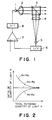
- a collimating lens 2 in front of a semiconductor laser light source 1 there is provided a collimating lens 2, whereby a divergent light beam emitted from said semiconductor laser light source 1 is converted into a parallel light beam. It is assumed that said light source 1 is so positioned that the junction plane of its active layer is perpendicular to the plane of drawing.
- converted laser beam is split into an outgoing light linearly transmitted and a monitoring light rectangularly reflected, by means of a beam splitter 3 having the characteristics to be explained later.
- the present embodiment employs a prism-shaped beam splitter, but there may also be utilized a plate-shaped beam splitter.
- the monitoring light beam split by reflection is concentrated by a condenser lens 4 onto a photodetector 5.
- the voltage is supplied to a voltage comparator 7 in which the voltage is compared with a reference input voltage composed of a light source drive signal such as pixel data corresponding to pixel density.
- the voltage comparator 7 is of a type capable of increasing/ decreasing the input reference voltage by comparison of two input voltages to thereby output, and effects current drive of the semiconductor laser light source 1 through a voltage-current converter 8.
- the above-explained arrangement performs so-called APC in which the intensity of the monitoring light beam detected by the photodetector 5 is compared with a predetermined intensity corresponding to the voltage of the drive signal by means of the voltage comparator 7, and the light output is maintained at a predetermined intensity by a feedback operation for increasing the drive current if the detected intensity is deficient or inversely decreasing the drive current if the detected intensity is excessive.
- the intensity ratio of the outgoing light to the monitoring light is not constant in the ordinary beam splitter employed in the present embodiment, of which reflectance and transmittance depend on the polarized state.
- the light polarized parallel to the plane of drawing will be called p-polarized light, while that polarized perpendicularly to said plane will be called s-polarized light thus distinguishing both lights.
- the laser oscillated light is mostly composed of s-polarized light, while the LED oscillated light is a random polarized light, that is a disordered polarized light containing p- and s-polarized lights in about same proportions.
- the light quantity ratio R of the quantity Pa of monitoring light reflected at the beam splitter 3 to the quantity Po of output light linearly transmitted through the beam splitter 3 can be represented as follows: where P is the total outgoing quantity of light emitted by the semiconductor laser 1; P p is the quantity of p-polarized component in said total outgoing quantity of light emitted; and R p and R s are reflectances of the beam splitter 3 for the p- and s-polarized components, respectively.
- the light quantity ratio R (1) monotonously increases in case of R s > R p , or (2) monotonously decreases in case of R s ⁇ R p .
- the proportion of the monitoring light quantity Pa decreases when the total emitted light quantity P is small, but the situation is inversed in case of (2).
- Fig. 2 shows the light quantity ratio R in the ordinate as a function of the total outgoing (emitted) light quantity P in the abscissa
- Fig. 3 shows the monitoring light quantity Pa in the ordinate as a function of the total emitted light quantity P in the abscissa.
- a beam splitter with property R s ⁇ R p allows a relative increase in the monitoring light quantity Pa when the total emitted light quantity P and the output light quantity Po are lower than those in the non-polarizing beam splitter, thereby improving the S/N ratio of photodetector 5.
- Fig. 4 is a partial schematic view of a modification of the foregoing embodiment, wherein a beam splitter 3' provides 9 transmitted light beam as the monitoring light and a reflected light beam as the output light.
- the junction of the active layer of the semiconductor laser 1 is positioned perpendicularly to the light-splitting plane of said beam splitter 3'.
- the beam splitter 3' has a property R s > R p
- the monitoring light quantity Pa can be increased when the total emitted light quantity P and the output light quantity Po are small, whereby the advantages as mentioned in the foregoing embodiment are obtained.
- the ordinary glass materials have the property R s > R p , the preparation of the beam splitter is even easier, with even lower cost, than said splitter 3 with property R s ⁇ R p .
- correction means for correcting non-linear characteristics of the beam splitter into linear.
- the non-linearity derived from not only characteristics of the beam splitter but also sensitivity characteristics of the recording medium, characteristics of the light source, characteristics of photodetector etc.
- the synthesized characteristics including the factors are preferably corrected linearly by the correction means.
- Said correction can be achieved, for example, by (1) correcting the reference voltage supplied to the voltage comparator 7 by means of a look-up table having a conversion characteristic capable of correcting said synthesized characteristics linearly, (2) giving predetermined non-linear conversion characteristics to the current-voltage converter 6 or the voltage-current converter 8 to correct linearly, or (3) providing a non-linear amplifier between the current-voltage converter 6 and the comparator 7 to correct linearly. Combinations of these methods may naturally be employed.
- the present invention can employ not only the semiconductor laser as shown in the foregoing embodiment, but also a light source which emits a light having mutually perpendicular polarized components with ratio of the components which is different depending on the total emitted light quantity.
- a light source which emits a light having mutually perpendicular polarized components with ratio of the components which is different depending on the total emitted light quantity.
- Examples of such light source include an Ar+ laser and a semiconductor-excited solid-state laser. This also applies to the following embodiments.
- Said first embodiment achieves improvements in performance such as an increase in the S/N ratio on detection of the monitoring light beam at a small quantity of light emitted from the source and an increase in extinction ratio of the emitted light, by positioning a photodetector in a light path at which a polarized component, perpendicular to the junction plane of the active layer of the semiconductor laser, is split in larger proportion.
- a beam splitter with property R s ⁇ R p is positioned as shown in Fig. 1.
- the present embodiment employs a beam splitter of property R s > R p in the same arrangement as shown in Fig. 1, or that of property R s ⁇ R p in the same arrangement as shown in Fig. 4.
- correction means for correcting the detected value of the monitoring light quantity Pa, in order to establish a linear relationship between the detected value and the output light quantity Pa.
- the semiconductor laser driving apparatus of the present embodiment allows to detect the variation in the total emitted light quantity P with high sensitivity, namely with high resolving power. This is because, in Fig. 3, the characteristic curve of the beam splitter with property R s > R p shows a steeper inclination (particularly when the total emitted light quantity P is small) than in other beem splitters, thus showing a larger change in the monitoring light quantity Pa for a given change in the total emitted light quantity P. Consequently, in the present embodiment it is possible to precisely control the light quantity from the semiconductor particularly when the total emitted light quantity P is small.
- the analog modulation in this range can only provide an extinction ratio (dynamic range) of 1:10, it is very difficult to record a halftone image of high definition on a recording material requiring a high extinction ratio such as a silver halide film.
- the semiconductor laser driving apparatus of the present embodiment provides a higher resolving power for the monitoring light quantity, and can therefore precisely control the output light quantity of the semiconductor laser, particularly in so-called LED light emission region with the light output of 1 mW or less, where the polarization ratio shows a large change.
- the present embodiment is advantageous for ordinary analog modulation.
- the first and second embodiments show examples of APC for maintaining a constant output of the laser by feedback of the output of the photodetector 5, but the light source driving apparatus of the present invention is effective also in an apparatus without APC proposed in said U.S. Patent Appln. S.N. 584,263.
- An embodiment relating to such apparatus without APC will be explained in the following. More detailed structures are described in said patent application.
- the structure is same as in Fig. 1 or 4, and the properity of the beam splitter is selected in the same manner as in the first or second embodiment.
- the semiconductor laser is modulated in the following manner.
- Fig. 5 shows the light output-current characteristic of a semiconductor laser.
- the slope efficiency n [mW/mA] scarcely changes by the temperature. That is, the lines in Fig. 5 are made with parallel displacement by a change in the temperature.
- certain semiconductor lasers show some change in the slope efficiency, any semiconductor laser of which slope efficiency can be regarded as constant at least within the temperature range of use can be employed in this embodiment.
- Fig. 6 shows the driving method for the semiconductor laser in the present embodiment, wherein P0 is the minimum light output of the semiconductor laser, and i0 is a driving current required to obtain said minimum light output P0 from the semiconductor laser at a temperature T1.
- the driving current for the semiconductor laser is linearly and gradually increased from i0, and the actual light output on this time is monitored with the photodector.
- the driving current is interrupted when the light output increases by P s from P0.
- the drive current need not be completely interrupted to zero, but can be reduced at least to a value lower than i0, thereby substantially interrupting the light ouput.
- a line 91 indicates the linearly increasing drive current
- a line 92 indicates the light output at temperature T1.
- the temperature of the semiconductor laser chip increases from T1 (lower temperature) to T2 (higher temperature).
- a temperature increase does not vary the slope efficiency of the semiconductor laser but only causes a parallel displacement of the lines indicating the light output-current characteristic.
- the minimum light output P0 does not vary but the drive current i0 for obtaining said minimum light output P0 varies. This is approximately the current providing a light output P0 in the light output-current characteristic parallel displaced to the temperature T2.
- the drive current i0' (> i0) represents a value required to obtain the light output P0 at the chip temperature T2 (> T1).
- a broken line 93 indicates the change in the light output when the drive current is linearly and gradually increased as in the equation (1).
- the laser oscillation starts from i0', and the drive current is interrupted when the light output increases by P s . Since the slope efficiency is constant as shown in Fig. 6, the sawtooth-shaped light output represented by the broken line 93 is identical with that at the temperature T1, so that the exposure is same as that represented by the equation (2).
- an exposure shown by the equation (2) is considered as the exposure for one pixel. Then, it will be undersood that a temperature change in the semiconductor laser does not cause the exposure in each pixel to be changed, but slightly displaces the position and time of exposure. More specifically, an increase in temperature causes a delay in exposure time, with inducing a shift of the exposure position to the rear. A decrease in temperature causes the contrary results. Thus, the change in exposure resulting from temperature change can be substantially corrected if said displacement in position and time is selected within the range of a pixel and less than the resolving power of human eyes.
- the exposure E may be regulated by a change in P s in the equation (2). It may also be achieved by a change in the inclination k with a constant P s , or by changes in k and P s . Also, as an alternative method, a light output equivalent to that in Fig. 6 may be obtained by detecting the minimum light output P0 with the photodetector to vary the exposure E by controlling the modulation time t based on the timing of said detection.
- the light modulation is so performed that light output of the semiconductor has a non-rectangular form, which includes such one that the light output increases gradually with time. Said modulation is performed until the desired exposure is reached, whereby a desired constant exposure independent of change in temperature is obtained without use of APC. Further, a high extinction ratio is obtained, so that a halftone image with a large gradation number (for example 4096 gradation) can be obtained. If a structure same as the first embodiment is employed in the present embodiment, the extinction ratio is large to thereby obtain an image with high contrast since the minimum light quantity (P0 in Fig. 6) in the gradual increase of light intensity is small. Also, if employed a structure same as the second embodiment, a large gradation number can be obtained since the resolving power of the monitoring light quantity is high.
- the semiconductor laser driving apparatus of the foregoing embodiments are applicable to a wide range of systems employing semiconductor laser, such as an image recording apparatus, an image reading apparatus, a display apparatus, an optical communication apparatus, a memory apparatus, a laser working apparatus, various measuring apparatus or the like.
- Fig. 7 illustrates, as an embodiment, a laser beam printer for recording a halftone image of multiple gradation by scanning a laser beam on a recording film. Such printer is principally used in medical applications in which high image quality is required.
- the beam splitter 3 is selected in the same manner as in the first or second embodiment.
- a semiconductor laser controller 9 incorporates a current-voltage converter 6, a voltage comparator 7, a voltage-current converter 8, a look-up table constituting the correction means etc. shown in Fig. 1, and effects the APC control as in the first or second embodiment or the control as in the third embodiment.
- a collimating lens 2 In a light path of the beam emitted by the semiconductor laser 1, there are provided a collimating lens 2, a beam splitter 3, a cylindrical lens 10 and a polygon mirror 11. In the reflecting direction of said polygon mirror 11, there are provided an f ⁇ lens 12, a mirror 13 and a recording film F. In the reflecting direction of the beam splitter 3, there are provided a condenser lens 4 and a photodetector 5.
- the recording film F is supplied from a supply magazine 14, transmitted by a roller 16 driven by a sub scanning motor 15, and received in a receiving magazine 17.
- a photodetector 18 is provided for a horizontal synchronisation signal.
- the semiconductor laser controller 9 effects modulation by controlling the oscillation intensity of the semiconductor laser 1 according to input image recording signals.
- a high gray scale modulation with as many as 4096 gradation is possible.
- Correction means (look-up table) in the controller 9 effects a correction so as to establish a linear relationship between the image density signals to be recorded and the image density recorded on the recording film.
- the non-linearity may be derived, for example, from the characteristics of the beam splitter, those of film sensitivity, those of light source and those of photodetector, but the overall synthesized characteristics are linearly corrected by said correction means.
- a laser beam L having a stable intensity obtained by APC explained in the first or second embodiment, or having a gradually increasing intensity explained in the third embodiment, is focused onto the polygon mirror 11 as a line through the cylindrical lens 10, and is put into a scanning motion by the rotation of the polygon mirror 11, and then is main-scanned on the photosensitive surface of the recording film F through the f ⁇ lens 12 and mirror 13.
- the sub scanning is achieved by transmitting the recording film F taken out from the supply magazine 14 in a direction substantially perpendicular to the main scanning direction by means of the sub scanning motor 15 and the roller 16. In this manner a two-dimensional latent image is recorded on the recording film F, which is subsequently stored in the receiving magazine 17.
- the present embodiment is not limited to the above-explained structure for directly recording an image on the recording film F, but is likewise applicable to so-called electrophotographic printer or copying machine.
- a laser beam is main-scanned by a scanning optical system similar to that explained above to record with exposure on photosensitive drum rotated in the sub scanning direction, whereby the content of the drum is transferred onto a recording sheet or the like to obtain a hard copy.
- a light source driving apparatus provided with a light generating unit including a light source and emitting a light component polarized in a predetermined direction and another light component polarized in the perpendicular direction in varying ratio depending on the total emitted light output; a light splitter for splitting the two polarized components in different splitting ratios into first and second light paths; a photodetector for detecting the light intensity in the first light path; and a control unit for controlling the light generating unit so as to maintain the light intensity in the second light path at a predetermined state, based on the detection output of the photodetector.
Landscapes
- Physics & Mathematics (AREA)
- Optics & Photonics (AREA)
- General Physics & Mathematics (AREA)
- Engineering & Computer Science (AREA)
- Multimedia (AREA)
- Signal Processing (AREA)
- Laser Beam Printer (AREA)
- Semiconductor Lasers (AREA)
- Exposure Or Original Feeding In Electrophotography (AREA)
- Fax Reproducing Arrangements (AREA)
- Dot-Matrix Printers And Others (AREA)
Applications Claiming Priority (4)
| Application Number | Priority Date | Filing Date | Title |
|---|---|---|---|
| JP16754890 | 1990-06-26 | ||
| JP167548/90 | 1990-06-26 | ||
| JP3174524A JPH04355986A (ja) | 1990-06-26 | 1991-06-19 | 光源駆動装置及びこの光源駆動装置を使用する装置 |
| JP174524/91 | 1991-06-19 |
Publications (3)
| Publication Number | Publication Date |
|---|---|
| EP0464556A2 true EP0464556A2 (fr) | 1992-01-08 |
| EP0464556A3 EP0464556A3 (en) | 1992-04-29 |
| EP0464556B1 EP0464556B1 (fr) | 1996-03-27 |
Family
ID=26491555
Family Applications (1)
| Application Number | Title | Priority Date | Filing Date |
|---|---|---|---|
| EP91110371A Expired - Lifetime EP0464556B1 (fr) | 1990-06-26 | 1991-06-24 | Appareil de commande d'une source de lumière et système de formation d'images utilisant un tel appareil |
Country Status (4)
| Country | Link |
|---|---|
| US (1) | US5282217A (fr) |
| EP (1) | EP0464556B1 (fr) |
| JP (1) | JPH04355986A (fr) |
| DE (1) | DE69118251T2 (fr) |
Cited By (4)
| Publication number | Priority date | Publication date | Assignee | Title |
|---|---|---|---|---|
| EP0677731A3 (fr) * | 1994-03-25 | 1996-02-07 | Omron Tateisi Electronics Co | Dispositif capteur optique. |
| FR2734902A1 (fr) * | 1995-05-30 | 1996-12-06 | Asahi Optical Co Ltd | Dispositif de commande d'intensite de lumiere |
| EP0804015A3 (fr) * | 1996-04-22 | 1997-11-05 | Canon Kabushiki Kaisha | Dispositif de balayage optique |
| EP0676658A3 (fr) * | 1994-04-11 | 1998-01-14 | Canon Kabushiki Kaisha | Système de balayage optique |
Families Citing this family (8)
| Publication number | Priority date | Publication date | Assignee | Title |
|---|---|---|---|---|
| US5774222A (en) * | 1994-10-07 | 1998-06-30 | Hitachi, Ltd. | Manufacturing method of semiconductor substrative and method and apparatus for inspecting defects of patterns on an object to be inspected |
| US5774486A (en) * | 1996-04-30 | 1998-06-30 | Motorola, Inc. | Waveguide power monitoring system for vertical cavity surface emitting lasers |
| US6134011A (en) * | 1997-09-22 | 2000-10-17 | Hdi Instrumentation | Optical measurement system using polarized light |
| DE19928171B4 (de) * | 1999-06-19 | 2011-01-05 | Leybold Optics Gmbh | Verfahren zur kontinuierlichen Bestimmung der optischen Schichtdicke von Beschichtungen |
| JP4690569B2 (ja) * | 2001-04-02 | 2011-06-01 | 日本オプネクスト株式会社 | 半導体レーザ装置及びそれを用いた光送信装置。 |
| JP2004342655A (ja) * | 2003-05-13 | 2004-12-02 | Brother Ind Ltd | レーザ制御装置およびそれを備えた画像形成装置 |
| US7206066B2 (en) * | 2004-03-19 | 2007-04-17 | Kla-Tencor Technologies Corporation | Reflectance surface analyzer |
| JPWO2006129757A1 (ja) | 2005-06-02 | 2009-01-08 | エスティーシー株式会社 | 半導体レーザ励起固体レーザ制御装置、及びこれを備えた半導体レーザ励起固体レーザ装置、並びにこれを備えた画像形成装置 |
Family Cites Families (11)
| Publication number | Priority date | Publication date | Assignee | Title |
|---|---|---|---|---|
| US4443695A (en) * | 1980-01-25 | 1984-04-17 | Canon Kabushiki Kaisha | Apparatus for controlling the quantity of light |
| JPS59129854A (ja) * | 1983-01-18 | 1984-07-26 | Dainippon Screen Mfg Co Ltd | 画像走査記録時における光量補正方法 |
| CA1251845A (fr) * | 1984-08-06 | 1989-03-28 | Ian D. Henning | Amplification optique |
| US4583128A (en) * | 1984-08-27 | 1986-04-15 | Minnesota Mining And Manufacturing Company | Continuous tone recording system incorporating feedback control circuit |
| JPH0728077B2 (ja) * | 1986-04-16 | 1995-03-29 | 株式会社トプコン | 半導体レ−ザ−の発振周波数・発振出力安定化装置 |
| US4844584A (en) * | 1986-06-26 | 1989-07-04 | Fuji Photo Film Co., Ltd. | Semiconductor laser beam splitting device |
| JPH01251681A (ja) * | 1988-03-25 | 1989-10-06 | Topcon Corp | 半導体レーザーの発振周波数・発振出力安定化装置 |
| US4942584A (en) * | 1988-06-22 | 1990-07-17 | Morihiro Karaki | Semiconductor laser apparatus driving system |
| JP2706262B2 (ja) * | 1988-07-12 | 1998-01-28 | キヤノン株式会社 | 半導体レーザ駆動装置 |
| JPH0273682A (ja) * | 1988-09-08 | 1990-03-13 | Nippon Digital Equip Kk | レーザダイオード駆動方法及び装置 |
| US5040896A (en) * | 1989-07-24 | 1991-08-20 | Behzad Moslehi | Three-crystal temperature-compensated reference interferometer for source wavelength stabilization |
-
1991
- 1991-06-19 JP JP3174524A patent/JPH04355986A/ja active Pending
- 1991-06-24 US US07/719,934 patent/US5282217A/en not_active Expired - Lifetime
- 1991-06-24 EP EP91110371A patent/EP0464556B1/fr not_active Expired - Lifetime
- 1991-06-24 DE DE69118251T patent/DE69118251T2/de not_active Expired - Fee Related
Cited By (8)
| Publication number | Priority date | Publication date | Assignee | Title |
|---|---|---|---|---|
| EP0677731A3 (fr) * | 1994-03-25 | 1996-02-07 | Omron Tateisi Electronics Co | Dispositif capteur optique. |
| EP0676658A3 (fr) * | 1994-04-11 | 1998-01-14 | Canon Kabushiki Kaisha | Système de balayage optique |
| US5963356A (en) * | 1994-04-11 | 1999-10-05 | Canon Kabushiki Kaisha | Scanning optical apparatus |
| FR2734902A1 (fr) * | 1995-05-30 | 1996-12-06 | Asahi Optical Co Ltd | Dispositif de commande d'intensite de lumiere |
| US5892219A (en) * | 1995-05-30 | 1999-04-06 | Asahi Kogaku Kogyo Kabushiki Kaisha | Light intensity controlling device |
| US6011250A (en) * | 1995-05-30 | 2000-01-04 | Asahi Kogaku Kogyo Kabushiki Kaisha | Light intensity controlling device |
| EP0804015A3 (fr) * | 1996-04-22 | 1997-11-05 | Canon Kabushiki Kaisha | Dispositif de balayage optique |
| US5991063A (en) * | 1996-04-22 | 1999-11-23 | Canon Kabushiki Kaisha | Optical scanning device |
Also Published As
| Publication number | Publication date |
|---|---|
| EP0464556A3 (en) | 1992-04-29 |
| EP0464556B1 (fr) | 1996-03-27 |
| DE69118251T2 (de) | 1996-09-05 |
| JPH04355986A (ja) | 1992-12-09 |
| US5282217A (en) | 1994-01-25 |
| DE69118251D1 (de) | 1996-05-02 |
Similar Documents
| Publication | Publication Date | Title |
|---|---|---|
| EP0464556B1 (fr) | Appareil de commande d'une source de lumière et système de formation d'images utilisant un tel appareil | |
| US4375067A (en) | Semiconductor laser device having a stabilized output beam | |
| JP3212153B2 (ja) | 可変波長光源を用いた光学出力装置でのスポット位置制御用の装置 | |
| US4950888A (en) | Scanning beam synchronization system | |
| JP2002040350A (ja) | 光走査装置 | |
| US4728989A (en) | Electrostatic latent image forming apparatus using semiconductor laser | |
| JP3212152B2 (ja) | 可変波長光源を用いた光学出力装置でのスポット位置制御方法 | |
| JP2715206B2 (ja) | レーザ記録装置 | |
| US5264869A (en) | Electro-optical control apparatus and system for spot position control in an optical output device | |
| CA2077813C (fr) | Dispositif et methode de commande de la position du spot dans un appareil de sortie utilisant un reseau lineaire de sources lumineuses | |
| US5461412A (en) | Method and apparatus for actively correcting curvature in the scan of an optical output device | |
| US5541761A (en) | Optical beam scanning apparatus adjusting focal point over entire image forming area by feedback control | |
| US5212381A (en) | Method of controlling slow scan direction of spot position in an optical output device employing an electro-optical control apparatus | |
| EP0293144A1 (fr) | Appareil de laser semi-conducteur | |
| JP2003215485A (ja) | 光学走査装置 | |
| US4699446A (en) | Dynamic power control for an external cavity stabilized laser diode in a holographic scanner | |
| JPH04200065A (ja) | 画像記録装置 | |
| EP0529918B1 (fr) | Dispositif optique de reproduction avec commande de la position de point | |
| EP0176329A2 (fr) | Diodes laser | |
| JP4853015B2 (ja) | 光走査装置及びこれを用いた画像形成装置 | |
| US4841314A (en) | Electrostatic latent image forming apparatus using semiconductor laser | |
| JP2767618B2 (ja) | レーザー走査光学装置 | |
| JP7710312B2 (ja) | 光走査装置、画像形成装置、制御方法、及び、プログラム | |
| JPH05160467A (ja) | 半導体レーザーのモードホッピング検出装置 | |
| JPH02168217A (ja) | 半導体レーザ走査装置 |
Legal Events
| Date | Code | Title | Description |
|---|---|---|---|
| PUAI | Public reference made under article 153(3) epc to a published international application that has entered the european phase |
Free format text: ORIGINAL CODE: 0009012 |
|
| AK | Designated contracting states |
Kind code of ref document: A2 Designated state(s): DE FR GB NL |
|
| PUAL | Search report despatched |
Free format text: ORIGINAL CODE: 0009013 |
|
| AK | Designated contracting states |
Kind code of ref document: A3 Designated state(s): DE FR GB NL |
|
| 17P | Request for examination filed |
Effective date: 19920911 |
|
| 17Q | First examination report despatched |
Effective date: 19940803 |
|
| GRAA | (expected) grant |
Free format text: ORIGINAL CODE: 0009210 |
|
| AK | Designated contracting states |
Kind code of ref document: B1 Designated state(s): DE FR GB NL |
|
| REF | Corresponds to: |
Ref document number: 69118251 Country of ref document: DE Date of ref document: 19960502 |
|
| ET | Fr: translation filed | ||
| GRAH | Despatch of communication of intention to grant a patent |
Free format text: ORIGINAL CODE: EPIDOS IGRA |
|
| PLBE | No opposition filed within time limit |
Free format text: ORIGINAL CODE: 0009261 |
|
| STAA | Information on the status of an ep patent application or granted ep patent |
Free format text: STATUS: NO OPPOSITION FILED WITHIN TIME LIMIT |
|
| 26N | No opposition filed | ||
| REG | Reference to a national code |
Ref country code: GB Ref legal event code: IF02 |
|
| PGFP | Annual fee paid to national office [announced via postgrant information from national office to epo] |
Ref country code: DE Payment date: 20080630 Year of fee payment: 18 Ref country code: NL Payment date: 20080618 Year of fee payment: 18 |
|
| PGFP | Annual fee paid to national office [announced via postgrant information from national office to epo] |
Ref country code: FR Payment date: 20080625 Year of fee payment: 18 |
|
| PGFP | Annual fee paid to national office [announced via postgrant information from national office to epo] |
Ref country code: GB Payment date: 20080627 Year of fee payment: 18 |
|
| GBPC | Gb: european patent ceased through non-payment of renewal fee |
Effective date: 20090624 |
|
| NLV4 | Nl: lapsed or anulled due to non-payment of the annual fee |
Effective date: 20100101 |
|
| REG | Reference to a national code |
Ref country code: FR Ref legal event code: ST Effective date: 20100226 |
|
| PG25 | Lapsed in a contracting state [announced via postgrant information from national office to epo] |
Ref country code: FR Free format text: LAPSE BECAUSE OF NON-PAYMENT OF DUE FEES Effective date: 20090630 |
|
| PG25 | Lapsed in a contracting state [announced via postgrant information from national office to epo] |
Ref country code: GB Free format text: LAPSE BECAUSE OF NON-PAYMENT OF DUE FEES Effective date: 20090624 |
|
| PG25 | Lapsed in a contracting state [announced via postgrant information from national office to epo] |
Ref country code: DE Free format text: LAPSE BECAUSE OF NON-PAYMENT OF DUE FEES Effective date: 20100101 |
|
| PG25 | Lapsed in a contracting state [announced via postgrant information from national office to epo] |
Ref country code: NL Free format text: LAPSE BECAUSE OF NON-PAYMENT OF DUE FEES Effective date: 20100101 |