EP0464620A2 - Bildinformationssteuergerät und Anzeigesystem - Google Patents
Bildinformationssteuergerät und Anzeigesystem Download PDFInfo
- Publication number
- EP0464620A2 EP0464620A2 EP91110530A EP91110530A EP0464620A2 EP 0464620 A2 EP0464620 A2 EP 0464620A2 EP 91110530 A EP91110530 A EP 91110530A EP 91110530 A EP91110530 A EP 91110530A EP 0464620 A2 EP0464620 A2 EP 0464620A2
- Authority
- EP
- European Patent Office
- Prior art keywords
- partial write
- partial
- writing
- memory units
- lines
- Prior art date
- Legal status (The legal status is an assumption and is not a legal conclusion. Google has not performed a legal analysis and makes no representation as to the accuracy of the status listed.)
- Granted
Links
Images


Classifications
-
- G—PHYSICS
- G09—EDUCATION; CRYPTOGRAPHY; DISPLAY; ADVERTISING; SEALS
- G09G—ARRANGEMENTS OR CIRCUITS FOR CONTROL OF INDICATING DEVICES USING STATIC MEANS TO PRESENT VARIABLE INFORMATION
- G09G3/00—Control arrangements or circuits, of interest only in connection with visual indicators other than cathode-ray tubes
- G09G3/20—Control arrangements or circuits, of interest only in connection with visual indicators other than cathode-ray tubes for presentation of an assembly of a number of characters, e.g. a page, by composing the assembly by combination of individual elements arranged in a matrix no fixed position being assigned to or needed to be assigned to the individual characters or partial characters
- G09G3/34—Control arrangements or circuits, of interest only in connection with visual indicators other than cathode-ray tubes for presentation of an assembly of a number of characters, e.g. a page, by composing the assembly by combination of individual elements arranged in a matrix no fixed position being assigned to or needed to be assigned to the individual characters or partial characters by control of light from an independent source
- G09G3/36—Control arrangements or circuits, of interest only in connection with visual indicators other than cathode-ray tubes for presentation of an assembly of a number of characters, e.g. a page, by composing the assembly by combination of individual elements arranged in a matrix no fixed position being assigned to or needed to be assigned to the individual characters or partial characters by control of light from an independent source using liquid crystals
- G09G3/3611—Control of matrices with row and column drivers
- G09G3/3648—Control of matrices with row and column drivers using an active matrix
- G09G3/3651—Control of matrices with row and column drivers using an active matrix using multistable liquid crystals, e.g. ferroelectric liquid crystals
-
- G—PHYSICS
- G09—EDUCATION; CRYPTOGRAPHY; DISPLAY; ADVERTISING; SEALS
- G09G—ARRANGEMENTS OR CIRCUITS FOR CONTROL OF INDICATING DEVICES USING STATIC MEANS TO PRESENT VARIABLE INFORMATION
- G09G3/00—Control arrangements or circuits, of interest only in connection with visual indicators other than cathode-ray tubes
- G09G3/20—Control arrangements or circuits, of interest only in connection with visual indicators other than cathode-ray tubes for presentation of an assembly of a number of characters, e.g. a page, by composing the assembly by combination of individual elements arranged in a matrix no fixed position being assigned to or needed to be assigned to the individual characters or partial characters
- G09G3/34—Control arrangements or circuits, of interest only in connection with visual indicators other than cathode-ray tubes for presentation of an assembly of a number of characters, e.g. a page, by composing the assembly by combination of individual elements arranged in a matrix no fixed position being assigned to or needed to be assigned to the individual characters or partial characters by control of light from an independent source
- G09G3/36—Control arrangements or circuits, of interest only in connection with visual indicators other than cathode-ray tubes for presentation of an assembly of a number of characters, e.g. a page, by composing the assembly by combination of individual elements arranged in a matrix no fixed position being assigned to or needed to be assigned to the individual characters or partial characters by control of light from an independent source using liquid crystals
- G09G3/3611—Control of matrices with row and column drivers
- G09G3/3622—Control of matrices with row and column drivers using a passive matrix
- G09G3/3629—Control of matrices with row and column drivers using a passive matrix using liquid crystals having memory effects, e.g. ferroelectric liquid crystals
-
- G—PHYSICS
- G09—EDUCATION; CRYPTOGRAPHY; DISPLAY; ADVERTISING; SEALS
- G09G—ARRANGEMENTS OR CIRCUITS FOR CONTROL OF INDICATING DEVICES USING STATIC MEANS TO PRESENT VARIABLE INFORMATION
- G09G2310/00—Command of the display device
- G09G2310/04—Partial updating of the display screen
Definitions
- the present invention relates to a display system and, more particularly, to an image information control apparatus for use in a display system using a ferroelectric liquid crystal having a memory function.
- a display panel using a ferroelectric liquid crystal (FLCD) imparted with a memory function is adopted in a PC or a WS, it is required to smoothly move, e.g., a mouse or a cursor to perform display.
- a moving display is realized by a partial writing system (in which only scan lines corresponding to an area to be partially rewritten are scanned) as disclosed in U.S. Patent No. 4,655,561.
- a partial writing system in which only scan lines corresponding to an area to be partially rewritten are scanned
- an image information control apparatus and a display system using the same comprising a partial write detector having at least two types of memory units for detecting and storing addresses accessed to a VRAM in units of lines in a scanning direction, thereby repeating the detection and the storage at different cycles, a circuit for performing calculations to recognize partial write information from contents of each of the memory units, memory units for storing the respective calculation results, a circuit for comparing the memory contents to determine a size relationship between partial write areas, a partial write ID signal controller for controlling a partial write ID signal on the basis of the size relationship between partial write areas and externally outputting the signal, and a circuit for, even when partial writing is being executed, forcibly interrupting the partial writing in accordance with a state of an external refresh control signal, starting refresh, and restarting the partial writing in accordance with a partial write state and a change in state of the refresh control signal.
- an image information control apparatus and a display system using the same wherein the partial write information detected in units of lines by the memory units are identified as continuous line address groups in the scan line direction from the accessed address data, the number of addresses, a start line address or an end line address, or the number of lines is calculated for each group, and a total number of accessed lines is calculated.
- an image information control apparatus and a display system using the same, wherein only access to the VRAM performed during writing is rendered valid.
- an image information control apparatus and a display system using the same wherein a detection period (sampling period) of the memory units for executing detection and storage in units of lines in the scan direction is shorter than a storage period thereof.
- an image information control apparatus and a display system using the same wherein when the size relationship between the partial write areas obtained from the partial write information is to be determined, a detection period (sampling period) of a memory unit having partial write information of a larger area is shorter than a storage period thereof.
- an image information control apparatus and a display system using the same wherein a cycle of determining the size relationship between the partial write areas obtained from the partial write information is synchronized with a cycle of the partial write detector for repeating detection and storage such that the cycles are integer multiples with respect to the different memory units, respectively.
- An apparatus and a system according to the present invention are suitable as a display using an FLCD (ferroelectric liquid crystal) imparted with a memory function and can allow use of both a partial writing method of realizing moving display such as a mouse or a cursor and a total-refresh scanning driving method.
- FLCD ferroelectric liquid crystal
- a partial writing method used in the present invention is basically performed as follows.
- Fig. 20 illustrates four events, i.e., three independent windows and a moving mouse font.
- a window 1 displays a clock
- a window 2 displays a rotationally moving line
- a window 3 displays vertical scrolling of characters.
- the respective windows have different display speeds and display asynchronous with each other (independent events). Since a one-line access time of an FLCD remains unchanged, provided that a temperature is constant, a time (scanning time) required to perform each window display by partial writing is proportional to the size of a partial write area. If partial writing is generated in one window while partial writing is executed in another, one of the windows partial writing of which is executed prior to the other must be determined.
- a priority order for partial writing operations must be predetermined when an event occurs so that the priority order is recognized to perform processing by predetermined procedures each time partial write request is generated. For example, the priority order is determined such that partial writing during scroll display is interrupted, clock display partial writing is performed, and then the interrupted partial writing is restarted, and procedures between the respective partial writing operations are determined accordingly.
- the concept of priority order is unsatisfactory in a multitask system such as a UNIX/X-Window.
- a multitask system such as a UNIX/X-Window.
- several requests simultaneously access partial writing and are stored in host queues (Fig. 19). Thereafter, these requests are transferred from the respective host queues to a queue buffer of a server either via a network or internally.
- the requests are set in the buffer of the server while their drawing order to a VRAM is held. Therefore, the priority order does not work well because the requests are processed in accordance with the drawing order. For example, although "mouse" has the highest priority, if a large number of image drawing requests to the VRAM are present before the mouse request, the mouse request is not executed until the foregoing requests are finished. That is, the mouse request cannot have the highest priority order in this multitask system (Fig. 20).
- This scheduler functions to give a proper priority order for partial writing to a request from a queue of a host (Fig. 21).
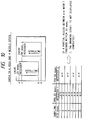
- Fig. 1 is a block diagram showing an apparatus of the present invention, in which a register for catching access information to a VRAM is illustrated. This information is transferred to an external circuit to count the number of partial writing operations or is transferred to another memory.
- This register adopts at-random inputs and serial outputs.
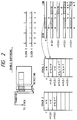
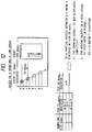
- Fig. 2 shows a multistack for obtaining a priority order in the present invention.
- a stack 1 stores a partial write area for every ⁇ t.
- a stack 2 basically stores a partial write area for every 2 ⁇ t in order to obtain a priority order.
- the depth level of each stack is not determined.
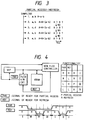
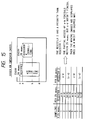
- Fig. 3 shows switching timings between partial writing and refresh in the present invention.
- a value B represents the number of switching times. If A exceeds B, all of partial writing operations must be interrupted to maintain a screen image by refresh.
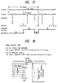
- Fig. 4 shows two signals PAR and REF for performing switching between partial writing and refresh in the present invention.
- a new GSP is controlling switching between partial writing and refresh.
- this partial write H/W supplies the signal PAR to a new FLCD controller, and the FLCD controller supplies the signal REF to the H/W to perform refresh, independently of each other.
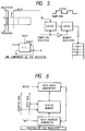
- Fig. 5 shows several hardware of the present invention. Although Fig. 5 is not correct, it provides a concept. Double buffers are preferably used in a sampling register and a memory register.
- Each register is constituted by a large number of F.F.s (Flip-Flops) or a static memory.
- a read register is serially reset (Fig. 5).
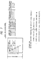
- Fig. 6 shows a static memory used in the present invention.
- An accessed line address is assigned to an address of the static memory.
- Data "1" is set at a memory address assigned to an accessed line address.
- control is performed such that an address is automatically assigned to an auto-address generator.
- an auto-data generator Upon resetting, an auto-data generator overwrites data "0" at all addresses of the memory while assigning addresses.
- a case 1 shown in Fig. 1 shows a practical multi-register arrangement. In this case, only one request is generated, and processing is performed at the highest speed.
- a case 2 shown in Fig. 8 shows another arrangement at a middle speed.
- a case 3 shown in Fig. 9 shows an arrangement at high and middle speeds.
- a case 4 shown in Fig. 10 shows an arrangement at a plurality of speeds. This arrangement has two windows which scroll at different speeds. This condition is strict for partial writing.
- a case 5 shown in Fig. 11 is similar to the case 4 except that the sizes and positions of two windows on a screen are different from each other. This condition is also strict for partial writing.
- a case 6 shown in Fig. 12 is similar to the case 3 except that the scroll speed of the case 6 is different from that in the case 3. This condition is also strict for partial writing.
- a case 7 shown in Fig. 13 is still another arrangement of the case 3, in which an improved method of obtaining a priority order is used.
- a case 8 shown in Fig. 14 is still another arrangement of the case 4. This arrangement has two windows which scroll at different speeds. Also in this case, an improved method of obtaining a priority order for partial writing is used.
- a case 9 shown in Fig. 15 shows another arrangement of the case 5, in which an improved method of obtaining a priority order is used. This case is no longer hard as compared with the foregoing partial writings.
- a case 10 shown in Fig. 16 shows another arrangement of the case 6, in which partial writing is no longer hard as compared with the foregoing cases. Also in this case, a timing chart shown in Fig. 17 is used.
- Fig. 17 shows a sequence and switching of actual partial writing and refresh in the present invention according to the arrangement shown in Fig. 16.
- FIG. 17 actual sampling timings of stacks 1 and 2 are shifted from each other. Access requests such as a-b, c-d, e-f, and g-h accompanying movement of a circle are detected in the sampling time of the stack 1, and scroll requests are detected in the sampling time of the stack 2. Since long partial writing has a priority to short one, the final result as partial write information is obtained as shown in Fig. 17.
- Fig. 18 shows a practical example for explaining an actual sampling H/W in an FLCD interface according to the timing chart shown Fig. 17.
- a scrolling image and a moving circle are present on a screen.
- a VRAM access time per bit is 100 nsec.
- a VRAM is constituted by 1 M x 8 bits.
- the size of the circle is 100 x 100 bits, and the scroll size is 1 K x 1 K bits. Therefore, times required for the moving circle and the scrolling window are 0.125 msec. and 12.5 msec., respectively.
- the circle moves every 25 msec., and scrolling is performed every 100 msec.
- Types of access to the VRAM are actually READ access and WRITE access. Strictly speaking, the WRITE access is actually required in terms of partial write control.
- Fig. 22 shows an example of copying one window to the other.
- a copy source window is accessed to the VRAM in a READ CYCLE
- a copy destination window is accessed in a WRITE CYCLE.
- partial writing is started at only the copy destination and need not be performed at the copy source.
- Partial writing is always performed after the access to the VRAM in the WRITE CYCLE and need not be performed in the READ CYCLE.
- the FLCD requires a scheduler under the multitask.
- long partial writing has a priority
- partial write data latched at the start timing of partial writing has a priority.
- another partial writing cycle is not accepted. Therefore, an order of actually generated partial write requests is uniformed during the sampling period, and partial writing operations are simultaneously executed thereafter. For this reason, a priority order of each event is converted into a size relationship between physical partial write areas by the hardware of item [1] above, and simultaneous partial writing operations are superposed within a certain period. Therefore, scheduling of the partial write request order at this timing is assumed to be completed.
- the FLCD partial writing mainly requires two items, and these two items must have the same function in the hardware interface.
- the item [1] is related to a priority order, and the item [2] is related to a scheduler.
- the scheduler of item [2] above has no clear arrangement but is included in the hardware of item [1] and has a function different therefrom.
- allocation of priority orders can be obtained by an H/W using the following procedures.
- B means a limited value with respect to the total number.
- B is probably smaller than the total number of scan lines because if B exceeds the total number, an access time for this partial writing exceeds a frame period. In other words, non-interlace is caused by partial writing over the frame period. For this reason, flicker is easily caused.
- the pixel size of the FLCD is 1,024 (vertical) x 1,280 (horizontal) and the frame frequency (refresh rate) at an ordinary use temperature is 20 Hz.
- the plurality of registers described above are designed to distinguish priority orders. However, a care must be paid to the cases 3 to 6 for allocating priority orders well.
- a register 3, if present, detects the third fastest movement of, e.g., every 100 msec. ( 10 Hz). Although it is assumed that a register 4 detects a movement of every 200 msec. or more, the register 4 is meaningless because refresh of the FLCD is performed at 20 Hz or less (50 msec. or more). The register 3 is unnecessary for the same reason.
- the fastest moving object is not continuously displayed but sometimes displayed or interlaced and displayed.
- the movement of the stack 1 is interlaced as in the case 7.
- the last invention about priority order allocation is an actual execution manner.
- partial write data is instantaneously detected by the register and stored during the sampling period.
- a certain period must be consumed in sampling.
- the FLCD must have a scheduler for requests simultaneously generated especially under the multitask. Therefore, the H/W FLCD interface operates, for example, as shown in Fig. 17.
- an actual sampling time of the stack 1 is 12.5 msec., and that of the stack 2 is 25 msec., i.e., twice that of the stack 1.
- the gates to the detectors are "ON". Each register detects and stores an accessed line address.
- the sampling interval of the stack 1 is 25 msec., and that of the stack 2 is 50 msec.
- Two images are present on a screen: one is an image of a circle moving at a high speed; and the other, a scrolling window.
- the access time of a VRAM per bit is 100 nsec/bit (this speed is considerably higher than other speeds). In this case, eight bits can be simultaneously accessed.
- one scroll full-screen access time is: Therefore, one-screen access of the window can be completely detected within the sampling time of 25 msec. of the stack 2.
- the scroll speed is 100 msec. while the sampling interval is 50 msec., partial writing of one scroll screen can be started after the detection.
- one moving display access cycle can be completely detected within the sampling time of 12.5 msec. of the stack 1.
- the sampling interval is 25 msec.
- at least one moving display partial writing cycle can be started for a circle having a moving speed of 25 msec.
- a scrolling window includes image information of a circle present on the screen. Partial writing of the circle moving during scrolling is displayed in accordance with information from the stack 1.
- the refresh is, of course, continued until the next partial writing is detected.
- compatibility with respect to a CRT display system is improved by simultaneously displaying partial scrolling and a mouse movement.
- An image information control apparatus includes a partial write detector having at least two types of memory units for detecting and storing addresses accessed to a VRAM in units of lines in a scanning direction, thereby repeating the detection and the storage at different cycles, a circuit for performing calculations to recognize partial write information from contents of each of the memory units, memory units for storing the respective calculation results, a circuit for comparing the memory contents to determine a size relationship between partial write areas, a partial write ID signal controller for controlling a partial write ID signal on the basis of the size relationship between partial write areas and externally outputting the signal, and a circuit for, even when partial writing is being executed, forcibly interrupting the partial writing in accordance with a state of an external refresh control signal, starting refresh, and restarting the partial writing in accordance with a partial write state and a change in state of the refresh control signal.
Landscapes
- Engineering & Computer Science (AREA)
- Physics & Mathematics (AREA)
- Computer Hardware Design (AREA)
- General Physics & Mathematics (AREA)
- Theoretical Computer Science (AREA)
- Crystallography & Structural Chemistry (AREA)
- Chemical & Material Sciences (AREA)
- Liquid Crystal Display Device Control (AREA)
- Control Of Indicators Other Than Cathode Ray Tubes (AREA)
- Selective Calling Equipment (AREA)
- Radar Systems Or Details Thereof (AREA)
- Liquid Crystal (AREA)
- Controls And Circuits For Display Device (AREA)
- Alarm Systems (AREA)
Applications Claiming Priority (2)
| Application Number | Priority Date | Filing Date | Title |
|---|---|---|---|
| JP171102/90 | 1990-06-27 | ||
| JP2171102A JP2840398B2 (ja) | 1990-06-27 | 1990-06-27 | 画像情報制御装置及び表示システム |
Publications (3)
| Publication Number | Publication Date |
|---|---|
| EP0464620A2 true EP0464620A2 (de) | 1992-01-08 |
| EP0464620A3 EP0464620A3 (en) | 1992-12-23 |
| EP0464620B1 EP0464620B1 (de) | 1996-11-20 |
Family
ID=15917018
Family Applications (1)
| Application Number | Title | Priority Date | Filing Date |
|---|---|---|---|
| EP91110530A Expired - Lifetime EP0464620B1 (de) | 1990-06-27 | 1991-06-26 | Bildinformationssteuergerät und Anzeigesystem |
Country Status (5)
| Country | Link |
|---|---|
| EP (1) | EP0464620B1 (de) |
| JP (1) | JP2840398B2 (de) |
| KR (1) | KR950012016B1 (de) |
| AT (1) | ATE145492T1 (de) |
| DE (1) | DE69123182T2 (de) |
Cited By (7)
| Publication number | Priority date | Publication date | Assignee | Title |
|---|---|---|---|---|
| EP0558342A1 (de) * | 1992-02-28 | 1993-09-01 | Canon Kabushiki Kaisha | Verfahren und Einrichtung zur Kontrolle einer Anzeigeeinheit |
| EP0573822A1 (de) * | 1992-05-19 | 1993-12-15 | Canon Kabushiki Kaisha | Verfahren und Einrichtung zur Steuerung einer Anzeige |
| EP0573821A1 (de) * | 1992-05-19 | 1993-12-15 | Canon Kabushiki Kaisha | Verfahren und Einrichtung zur Steuerung einer Anzeige |
| EP0608056A1 (de) * | 1993-01-11 | 1994-07-27 | Canon Kabushiki Kaisha | Anzeigelinienverteilungssystem |
| EP0608053A3 (de) * | 1993-01-11 | 1995-01-11 | Canon Kk | Farbanzeigevorrichtung. |
| AU672648B2 (en) * | 1993-01-11 | 1996-10-10 | Canon Kabushiki Kaisha | Display line dispatcher apparatus |
| CN102737589A (zh) * | 2011-03-29 | 2012-10-17 | 宏碁股份有限公司 | 用于液晶显示装置的控制方法及液晶显示装置 |
Family Cites Families (2)
| Publication number | Priority date | Publication date | Assignee | Title |
|---|---|---|---|---|
| AU617006B2 (en) * | 1988-09-29 | 1991-11-14 | Canon Kabushiki Kaisha | Data processing system and apparatus |
| AU634725B2 (en) * | 1988-10-31 | 1993-03-04 | Canon Kabushiki Kaisha | Display system |
-
1990
- 1990-06-27 JP JP2171102A patent/JP2840398B2/ja not_active Expired - Fee Related
-
1991
- 1991-06-26 DE DE69123182T patent/DE69123182T2/de not_active Expired - Fee Related
- 1991-06-26 EP EP91110530A patent/EP0464620B1/de not_active Expired - Lifetime
- 1991-06-26 AT AT91110530T patent/ATE145492T1/de not_active IP Right Cessation
- 1991-06-27 KR KR1019910010799A patent/KR950012016B1/ko not_active Expired - Fee Related
Cited By (12)
| Publication number | Priority date | Publication date | Assignee | Title |
|---|---|---|---|---|
| EP0558342A1 (de) * | 1992-02-28 | 1993-09-01 | Canon Kabushiki Kaisha | Verfahren und Einrichtung zur Kontrolle einer Anzeigeeinheit |
| US5717420A (en) * | 1992-02-28 | 1998-02-10 | Canon Kabushiki Kaisha | Display control apparatus and method |
| EP0573822A1 (de) * | 1992-05-19 | 1993-12-15 | Canon Kabushiki Kaisha | Verfahren und Einrichtung zur Steuerung einer Anzeige |
| EP0573821A1 (de) * | 1992-05-19 | 1993-12-15 | Canon Kabushiki Kaisha | Verfahren und Einrichtung zur Steuerung einer Anzeige |
| US5926159A (en) * | 1992-05-19 | 1999-07-20 | Canon Kabushiki Kaisha | Display control apparatus and method therefor capable of limiting an area for partial rewriting |
| US5929831A (en) * | 1992-05-19 | 1999-07-27 | Canon Kabushiki Kaisha | Display control apparatus and method |
| EP0608056A1 (de) * | 1993-01-11 | 1994-07-27 | Canon Kabushiki Kaisha | Anzeigelinienverteilungssystem |
| EP0608053A3 (de) * | 1993-01-11 | 1995-01-11 | Canon Kk | Farbanzeigevorrichtung. |
| AU672648B2 (en) * | 1993-01-11 | 1996-10-10 | Canon Kabushiki Kaisha | Display line dispatcher apparatus |
| US5576731A (en) * | 1993-01-11 | 1996-11-19 | Canon Inc. | Display line dispatcher apparatus |
| US5844532A (en) * | 1993-01-11 | 1998-12-01 | Canon Inc. | Color display system |
| CN102737589A (zh) * | 2011-03-29 | 2012-10-17 | 宏碁股份有限公司 | 用于液晶显示装置的控制方法及液晶显示装置 |
Also Published As
| Publication number | Publication date |
|---|---|
| ATE145492T1 (de) | 1996-12-15 |
| DE69123182T2 (de) | 1997-04-24 |
| DE69123182D1 (de) | 1997-01-02 |
| EP0464620A3 (en) | 1992-12-23 |
| EP0464620B1 (de) | 1996-11-20 |
| JP2840398B2 (ja) | 1998-12-24 |
| JPH0458221A (ja) | 1992-02-25 |
| KR920001418A (ko) | 1992-01-30 |
| KR950012016B1 (ko) | 1995-10-13 |
Similar Documents
| Publication | Publication Date | Title |
|---|---|---|
| US5357267A (en) | Image information control apparatus and display system | |
| US5500654A (en) | VGA hardware window control system | |
| US5146558A (en) | Data processing system and apparatus | |
| US5760789A (en) | Method for processing and prioritizing display of data from various sources | |
| US5374941A (en) | Display control apparatus for dispersionless display | |
| EP0526098B1 (de) | Ablauffolgeplanung von Zeichenbefehlen in einem multitasking Datenverarbeitungssystem | |
| EP0464620B1 (de) | Bildinformationssteuergerät und Anzeigesystem | |
| EP0573821A1 (de) | Verfahren und Einrichtung zur Steuerung einer Anzeige | |
| US5717906A (en) | Frame comparison with reduced memory via changed scanline detection and post-addition rotational shifting | |
| CA2167755C (en) | Device synchronization on a graphics accelerator | |
| JPH07234773A (ja) | 表示制御装置 | |
| JPH0566733A (ja) | 表示制御装置 | |
| US5751277A (en) | Image information control apparatus and display system | |
| JP3140803B2 (ja) | 表示制御装置および表示制御方法 | |
| JP3322109B2 (ja) | 表示制御装置 | |
| KR950012015B1 (ko) | 화상정보제어장치 | |
| JP3229341B2 (ja) | 表示制御装置および表示制御方法 | |
| JPH0566732A (ja) | 表示制御装置 | |
| JP3043378B2 (ja) | 表示制御装置および表示制御方法 | |
| JP3043379B2 (ja) | 表示制御装置および表示制御方法 | |
| JP3264520B2 (ja) | 表示制御装置 | |
| JP3109892B2 (ja) | 表示制御装置及び方法 | |
| JP3262361B2 (ja) | 表示制御装置及び方法 | |
| JP2861159B2 (ja) | ウィンドウ表示制御装置 | |
| JPS6374090A (ja) | 文字発生器のアクセス方式 |
Legal Events
| Date | Code | Title | Description |
|---|---|---|---|
| PUAI | Public reference made under article 153(3) epc to a published international application that has entered the european phase |
Free format text: ORIGINAL CODE: 0009012 |
|
| AK | Designated contracting states |
Kind code of ref document: A2 Designated state(s): AT BE CH DE DK ES FR GB GR IT LI LU NL SE |
|
| PUAL | Search report despatched |
Free format text: ORIGINAL CODE: 0009013 |
|
| AK | Designated contracting states |
Kind code of ref document: A3 Designated state(s): AT BE CH DE DK ES FR GB GR IT LI LU NL SE |
|
| 17P | Request for examination filed |
Effective date: 19930505 |
|
| 17Q | First examination report despatched |
Effective date: 19941110 |
|
| GRAG | Despatch of communication of intention to grant |
Free format text: ORIGINAL CODE: EPIDOS AGRA |
|
| GRAH | Despatch of communication of intention to grant a patent |
Free format text: ORIGINAL CODE: EPIDOS IGRA |
|
| GRAH | Despatch of communication of intention to grant a patent |
Free format text: ORIGINAL CODE: EPIDOS IGRA |
|
| GRAA | (expected) grant |
Free format text: ORIGINAL CODE: 0009210 |
|
| AK | Designated contracting states |
Kind code of ref document: B1 Designated state(s): AT BE CH DE DK ES FR GB GR IT LI LU NL SE |
|
| PG25 | Lapsed in a contracting state [announced via postgrant information from national office to epo] |
Ref country code: LI Effective date: 19961120 Ref country code: GR Free format text: LAPSE BECAUSE OF FAILURE TO SUBMIT A TRANSLATION OF THE DESCRIPTION OR TO PAY THE FEE WITHIN THE PRESCRIBED TIME-LIMIT Effective date: 19961120 Ref country code: ES Free format text: THE PATENT HAS BEEN ANNULLED BY A DECISION OF A NATIONAL AUTHORITY Effective date: 19961120 Ref country code: DK Effective date: 19961120 Ref country code: CH Effective date: 19961120 Ref country code: BE Effective date: 19961120 Ref country code: AT Effective date: 19961120 |
|
| REF | Corresponds to: |
Ref document number: 145492 Country of ref document: AT Date of ref document: 19961215 Kind code of ref document: T |
|
| REF | Corresponds to: |
Ref document number: 69123182 Country of ref document: DE Date of ref document: 19970102 |
|
| ET | Fr: translation filed | ||
| ITF | It: translation for a ep patent filed | ||
| REG | Reference to a national code |
Ref country code: CH Ref legal event code: PL |
|
| PG25 | Lapsed in a contracting state [announced via postgrant information from national office to epo] |
Ref country code: LU Free format text: LAPSE BECAUSE OF NON-PAYMENT OF DUE FEES Effective date: 19970630 |
|
| PLBE | No opposition filed within time limit |
Free format text: ORIGINAL CODE: 0009261 |
|
| STAA | Information on the status of an ep patent application or granted ep patent |
Free format text: STATUS: NO OPPOSITION FILED WITHIN TIME LIMIT |
|
| 26N | No opposition filed | ||
| REG | Reference to a national code |
Ref country code: GB Ref legal event code: IF02 |
|
| PGFP | Annual fee paid to national office [announced via postgrant information from national office to epo] |
Ref country code: SE Payment date: 20030604 Year of fee payment: 13 |
|
| PGFP | Annual fee paid to national office [announced via postgrant information from national office to epo] |
Ref country code: FR Payment date: 20030610 Year of fee payment: 13 |
|
| PGFP | Annual fee paid to national office [announced via postgrant information from national office to epo] |
Ref country code: GB Payment date: 20030625 Year of fee payment: 13 |
|
| PGFP | Annual fee paid to national office [announced via postgrant information from national office to epo] |
Ref country code: NL Payment date: 20030630 Year of fee payment: 13 |
|
| PGFP | Annual fee paid to national office [announced via postgrant information from national office to epo] |
Ref country code: DE Payment date: 20030707 Year of fee payment: 13 |
|
| PG25 | Lapsed in a contracting state [announced via postgrant information from national office to epo] |
Ref country code: GB Free format text: LAPSE BECAUSE OF NON-PAYMENT OF DUE FEES Effective date: 20040626 |
|
| PG25 | Lapsed in a contracting state [announced via postgrant information from national office to epo] |
Ref country code: SE Free format text: LAPSE BECAUSE OF NON-PAYMENT OF DUE FEES Effective date: 20040627 |
|
| PG25 | Lapsed in a contracting state [announced via postgrant information from national office to epo] |
Ref country code: NL Free format text: LAPSE BECAUSE OF NON-PAYMENT OF DUE FEES Effective date: 20050101 Ref country code: DE Free format text: LAPSE BECAUSE OF NON-PAYMENT OF DUE FEES Effective date: 20050101 |
|
| EUG | Se: european patent has lapsed | ||
| EUG | Se: european patent has lapsed | ||
| GBPC | Gb: european patent ceased through non-payment of renewal fee |
Effective date: 20040626 |
|
| PG25 | Lapsed in a contracting state [announced via postgrant information from national office to epo] |
Ref country code: FR Free format text: LAPSE BECAUSE OF NON-PAYMENT OF DUE FEES Effective date: 20050228 |
|
| NLV4 | Nl: lapsed or anulled due to non-payment of the annual fee |
Effective date: 20050101 |
|
| REG | Reference to a national code |
Ref country code: FR Ref legal event code: ST |
|
| PG25 | Lapsed in a contracting state [announced via postgrant information from national office to epo] |
Ref country code: IT Free format text: LAPSE BECAUSE OF NON-PAYMENT OF DUE FEES;WARNING: LAPSES OF ITALIAN PATENTS WITH EFFECTIVE DATE BEFORE 2007 MAY HAVE OCCURRED AT ANY TIME BEFORE 2007. THE CORRECT EFFECTIVE DATE MAY BE DIFFERENT FROM THE ONE RECORDED. Effective date: 20050626 |