EP0464667A2 - Circuit générateur d'un signal de remise à zéro à la mise sous tension - Google Patents
Circuit générateur d'un signal de remise à zéro à la mise sous tension Download PDFInfo
- Publication number
- EP0464667A2 EP0464667A2 EP91110651A EP91110651A EP0464667A2 EP 0464667 A2 EP0464667 A2 EP 0464667A2 EP 91110651 A EP91110651 A EP 91110651A EP 91110651 A EP91110651 A EP 91110651A EP 0464667 A2 EP0464667 A2 EP 0464667A2
- Authority
- EP
- European Patent Office
- Prior art keywords
- power
- mos transistor
- signal generating
- generating circuit
- clear signal
- Prior art date
- Legal status (The legal status is an assumption and is not a legal conclusion. Google has not performed a legal analysis and makes no representation as to the accuracy of the status listed.)
- Withdrawn
Links
- 239000003990 capacitor Substances 0.000 description 26
- 230000007423 decrease Effects 0.000 description 7
- 238000010586 diagram Methods 0.000 description 5
- 238000009413 insulation Methods 0.000 description 4
- 239000004065 semiconductor Substances 0.000 description 4
- 239000004020 conductor Substances 0.000 description 3
- 238000004519 manufacturing process Methods 0.000 description 2
- 238000000034 method Methods 0.000 description 2
- 230000000630 rising effect Effects 0.000 description 2
- 239000000758 substrate Substances 0.000 description 2
- 238000009792 diffusion process Methods 0.000 description 1
- 230000003628 erosive effect Effects 0.000 description 1
- 230000007257 malfunction Effects 0.000 description 1
- 230000002035 prolonged effect Effects 0.000 description 1
- 229920006395 saturated elastomer Polymers 0.000 description 1
Images



Classifications
-
- H—ELECTRICITY
- H03—ELECTRONIC CIRCUITRY
- H03K—PULSE TECHNIQUE
- H03K17/00—Electronic switching or gating, i.e. not by contact-making and –breaking
- H03K17/22—Modifications for ensuring a predetermined initial state when the supply voltage has been applied
- H03K17/223—Modifications for ensuring a predetermined initial state when the supply voltage has been applied in field-effect transistor switches
-
- H—ELECTRICITY
- H03—ELECTRONIC CIRCUITRY
- H03K—PULSE TECHNIQUE
- H03K17/00—Electronic switching or gating, i.e. not by contact-making and –breaking
Definitions
- the present invention relates to a power-on-clear signal generating circuit which generates a power-on-clear signal when the power is turned on.
- the internal status (how it has been set) of the resistor, etc. thereof cannot be observed at the time when the power is turned on; therefore, the internal state of the resistor, etc. having been set so, is reset upon turning on the power by a power-on-clear signal generated from the power-on-clear signal generating circuit usually provided in the IC device.
- Fig. 1 depicts a conventional power-on-clear signal generating circuit.
- the source-drain path of a P-channel MOS transistor 11, and a capacitor 12 is connected in series and inserted between a node to which a power voltage VDD is applied and another node to which a ground voltage GND is applied.
- the gate of the MOS transistor 11 is connected to the GND node, and this transistor 11 is conductive at any time.
- the above capacitor 12 is provided so as to set a delay time, which is defined as a time period between the turning-on of the power and the inversion of the level of a power-on-clear signal POC.
- the capacitor 12 is composed of a depression type MOS transistor; therefore, its capacitance is fixed.
- the time required for charging the capacitor 12 changes, accordingly.
- the time required for the potential of the node A to reach the circuit threshold voltage of the Schmitt trigger circuit 13 varies, affecting a predetermined power-on-clear time period set by the capacitor 12.
- the value of the power voltage VDD drops, the drain current of the MOS transistor 11 decreases, accordingly, thereby delaying the rising of the potential of the node A while the capacitor 12 is being charged. This results in prolongation of the power-on-clear time period, and in some cases, the time period is prolonged twice as long as the set value, depending on the variance of the power voltage VDD.
- the present invention has been achieved in consideration of the above, and the purpose thereof is to provide a power-on-clear signal generating circuit which can maintain its power-on-clear time period at approximately constant all the time even if the power voltage varies.
- a power-on-clear signal generating circuit comprising the first power source node to which the first power source voltage is applied, the second power source node to which the second power source voltage is applied, a load element an end of which is connected to the first power source node, and the first MOS transistor of the enhancement type, a gate of which is connected to an other end of said load element, and a source and drain of which are connected to the second power source node.
- a power-on-clear signal generating circuit comprising the first power source node to which the first power source voltage is applied, the second power source node to which the second power source voltage is applied, the load element an end of which is connected to the first power source node, the first MOS transistor of the enhancement type, a gate of which is connected to an other end of said load element, and a source and drain of which are connected to said second power source node, and a signal generating circuit for outputting a power-on-clear signal, an input terminal of which is connected to a connection node between said load element and the gate of said first MOS transistor so as to receive a signal from the connection node at a predetermined circuit threshold voltage.
- Fig. 2 shows the structure of the first embodiment of the power-on-clear signal generating circuit according to the present invention.
- the source and the back gate of an enhancement type P-channel MOS transistor 22, which functions as a load element are connected to a node 21 to which a positive power voltage VDD is applied, and the gate of an enhancement type N-channel MOS transistor 23, which functions as a capacitor, is connected to the drain of the MOS transistor 22.
- All of the source, drain, and back gate of the MOS transistor 23 are connected to a node 24 to which a ground voltage GND is applied.
- the gate of the MOS transistor 22 is connected to the node 24 of the ground voltage GND; therefore the MOS transistor 22 is at any time conductive.
- the input terminal of the Schmitt trigger circuit 25 is connected to the node A to which the drain of the MOS transistor 22 and the gate of the MOS transistor 23 are connected.
- the output terminal of the Schmitt trigger circuit 25 is connected to an output terminal 26 for outputting a power-on-clear signal POC.
- a power voltage VDD of the positive polarity type and a ground voltage GND are supplied also to the Schmitt trigger circuit 25.
- Fig. 4 shows the structure of the enhancement type N-channel MOS transistor 23, illustrating an N type semiconductor substrate 31, and p type well region 32.
- a source region 33 and a drain region 34 both of which are N+ type diffusion regions are formed as they are apart from each other.
- a gate electrode conductor 36 is provided indirectly via a gate insulation film 35.
- a depletion layer 37 is created in the channel region.
- Fig. 4 depicts the transistor before an inversion layer is formed in its channel region. Since a carrier is not present in the depletion layer 37, it can be regarded as an insulation layer 37.
- the gate capacitor of the MOS transistor 23 can be regarded as a combination of a capacitor Cj, i.e. the depletion layer 37 and a capacitor Cox, i.e. the gate insulation film 35.
- expansion of the depletion layer 37 depends on the level of the potential VG supplied to the gate electrode conductor 36.
- the drain current flowing into the MOS transistor 22 varies, accordingly.
- the rate of variance of the drain current into the MOS transistor 22 due to the variance of the power voltage VDD is significantly higher than that of the circuit threshold voltage of the Schmitt trigger circuit 25.
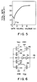
- the gate-source voltage of the MOS transistor 22 drops, and the drain current decreases. Consequently, the rising speed of the gate potential of the MOS transistor 23 becomes slower than in the case where the power voltage is at the standard level. Further, the gate capacitance of the MOS transistor 23 varies in accordance with the rise of the gate potential, as can be seen in Fig. 5. In other words, in the case where the gate voltage is the same as or higher than the MOS transistor's threshold voltage VTH, the gate capacitance decreases.
- the time required until the potential of the node A reaches the circuit threshold voltage of the Schmitt trigger circuit 25 from the point of turning on of the power does not deviates from that of the case where the power voltage is at the standard level, despite that the power voltage VDD drops and the drain current of the MOS transistor 22 decreases.
- the time required until the potential of the node A reaches the circuit threshold voltage of the Schmitt trigger circuit 25 from the point of turning on of the power also does not deviate from that of the case where the power voltage is at the standard level.
- Fig. 6 shows a detailed structure of a Schmitt trigger circuit 25 employed in the above embodiment.
- the source-drain paths of two P-channel MOS transistors 41 and 42, and two N-channel MOS transistors 43 and 44 are inserted in series between a node to which a positive polar power potential VDD is applied, and another node to which a ground voltage GND is applied. Further, the gates of the MOS transistors 41-44 are connected in common with each other to make the input terminal of this Schmitt trigger circuit.
- the source-drain path of a P-channel MOS transistor 46 is inserted between a connection node 45 for connecting the MOS transistors 41 and 42 in series to each other and a node to which a ground voltage GND is applied, whereas the source-drain path of the N-channel MOS transistor 48 is inserted between a connection node 47 for connecting the MOS transistors 43 and 44 in series to each other and a node to which a power voltage VDD is applied.
- an input terminal of an inverter 50 is connected to the series connection node 49 of the MOS transistors 42 and 43, and this output terminal is connected to a input terminal of an inverter 51.
- An output terminal of the inverter 51 is connected to an output terminal 26 from where the power-on-clear signal POC is output, and the gates of both MOS transistors 46 and 48 are connected to the output terminal of the inverter 51.
- the Schmitt trigger circuit having such a structure is well-known in the field of the semiconductor integrated circuit devices.
- a circuit threshold voltage VTHCH at which an input signal raises its level from “L” to “H” differs from a circuit threshold voltage VTHCL at which an input signal lowers its level from “H” to “L”, and more specifically, the circuit threshold voltage VTHCH is higher than the circuit threshold voltage VTHCL.
- the power-on-clear signal generating circuit employs the enhancement type MOS transistor 23 as a capacitor.
- the MOS transistor 23 can be formed through a process similar to those for the other enhancement type MOS transistors of the circuit. Therefore, manufacture of such a circuit can be conducted without adding any extra process to the conventional manufacturing method.
- the above embodiment is a very advantageous circuit consisting of enhancement type MOS transistors, which is presently most available.
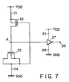
- FIG. 7 the second embodiment of the present invention is depicted in Fig. 7, in which an inverter 27 is employed in place of the Schmitt trigger circuit 25 in the first embodiment, to generate a power-on-clear signal POC in accordance with a signal from the node A.
- a buffer circuit 28 is employed in place of the Schmitt trigger circuit 25 in the first embodiment, to generate a power-on-clear signal POC in accordance with a signal from the node A.
- the present invention is of course not limited to the above-mentioned two embodiments, and can be remodeled into a variety of circuits.
- the enhancement type MOS transistor 22 is used as a load element; however resistors, etc. can be used as such a load element in place of the MOS transistors.
- a power-on-clear signal generating circuit which is able to maintain a substantially constant clear time period at any time if a power voltage varies.
Landscapes
- Electronic Switches (AREA)
- Semiconductor Integrated Circuits (AREA)
- Metal-Oxide And Bipolar Metal-Oxide Semiconductor Integrated Circuits (AREA)
- Manipulation Of Pulses (AREA)
- Logic Circuits (AREA)
Applications Claiming Priority (2)
| Application Number | Priority Date | Filing Date | Title |
|---|---|---|---|
| JP2171212A JPH0458555A (ja) | 1990-06-28 | 1990-06-28 | パワーオンリセット回路 |
| JP171212/90 | 1990-06-28 |
Publications (2)
| Publication Number | Publication Date |
|---|---|
| EP0464667A2 true EP0464667A2 (fr) | 1992-01-08 |
| EP0464667A3 EP0464667A3 (en) | 1992-04-22 |
Family
ID=15919117
Family Applications (1)
| Application Number | Title | Priority Date | Filing Date |
|---|---|---|---|
| EP19910110651 Withdrawn EP0464667A3 (en) | 1990-06-28 | 1991-06-27 | Power-on-clear signal generating circuit |
Country Status (3)
| Country | Link |
|---|---|
| EP (1) | EP0464667A3 (fr) |
| JP (1) | JPH0458555A (fr) |
| KR (1) | KR920001841A (fr) |
Cited By (2)
| Publication number | Priority date | Publication date | Assignee | Title |
|---|---|---|---|---|
| US5999039A (en) * | 1996-09-30 | 1999-12-07 | Advanced Micro Devices, Inc. | Active power supply filter |
| CN120601877A (zh) * | 2025-08-11 | 2025-09-05 | 合肥市山海半导体技术有限公司 | 一种唤醒器电路及电子设备 |
Families Citing this family (1)
| Publication number | Priority date | Publication date | Assignee | Title |
|---|---|---|---|---|
| KR100471072B1 (ko) | 2002-07-20 | 2005-03-10 | 삼성전자주식회사 | 제빵기 |
Family Cites Families (2)
| Publication number | Priority date | Publication date | Assignee | Title |
|---|---|---|---|---|
| US4717840A (en) * | 1986-03-14 | 1988-01-05 | Western Digital Corporation | Voltage level sensing power-up reset circuit |
| US4902910A (en) * | 1987-11-17 | 1990-02-20 | Xilinx, Inc. | Power supply voltage level sensing circuit |
-
1990
- 1990-06-28 JP JP2171212A patent/JPH0458555A/ja active Pending
-
1991
- 1991-06-27 KR KR1019910010794A patent/KR920001841A/ko not_active Ceased
- 1991-06-27 EP EP19910110651 patent/EP0464667A3/en not_active Withdrawn
Cited By (2)
| Publication number | Priority date | Publication date | Assignee | Title |
|---|---|---|---|---|
| US5999039A (en) * | 1996-09-30 | 1999-12-07 | Advanced Micro Devices, Inc. | Active power supply filter |
| CN120601877A (zh) * | 2025-08-11 | 2025-09-05 | 合肥市山海半导体技术有限公司 | 一种唤醒器电路及电子设备 |
Also Published As
| Publication number | Publication date |
|---|---|
| JPH0458555A (ja) | 1992-02-25 |
| KR920001841A (ko) | 1992-01-30 |
| EP0464667A3 (en) | 1992-04-22 |
Similar Documents
| Publication | Publication Date | Title |
|---|---|---|
| US7554379B2 (en) | High-speed, low-power level shifter for mixed signal-level environments | |
| JP2797844B2 (ja) | 半導体集積回路 | |
| KR0162931B1 (ko) | 저 소비 전류로 동작하는 파워-온 신호 발생회로 | |
| US7990667B2 (en) | Semiconductor device including esd protection field effect transistor with adjustable back gate potential | |
| EP0405319B1 (fr) | Circuit de retard présentant un retard stable | |
| KR960003529B1 (ko) | 반도체 메모리 장치의 칩 초기화 신호 발생회로 | |
| US7834677B2 (en) | Transmission gate with body effect compensation circuit | |
| JPS636918A (ja) | Cmos−入力回路 | |
| US4725746A (en) | MOSFET buffer circuit with an improved bootstrapping circuit | |
| US7482847B2 (en) | Power-on reset circuit | |
| JPH05168151A (ja) | 電源投入検出回路 | |
| US5239211A (en) | Output buffer circuit | |
| US6380792B1 (en) | Semiconductor integrated circuit | |
| JPS583325A (ja) | インバ−タ回路 | |
| US4529889A (en) | Sense amplifier latch voltage waveform generator circuit | |
| KR910003604B1 (ko) | 차아지업 및 디스차아지 회로를 이용한 기준전압 발생회로 | |
| JP3025921B2 (ja) | パワーオンリセット回路 | |
| US4525640A (en) | High performance and gate having an "natural" or zero threshold transistor for providing a faster rise time for the output | |
| JPS6358493B2 (fr) | ||
| JPS6217896B2 (fr) | ||
| JP2544157B2 (ja) | 半導体集積回路装置 | |
| JPH0753308Y2 (ja) | イニシャルクリア回路 | |
| GB2203308A (en) | Reducing transient noise in output driver IC | |
| JPH0529910A (ja) | 論理回路 | |
| JPS59158129A (ja) | 半導体集積回路装置 |
Legal Events
| Date | Code | Title | Description |
|---|---|---|---|
| PUAI | Public reference made under article 153(3) epc to a published international application that has entered the european phase |
Free format text: ORIGINAL CODE: 0009012 |
|
| 17P | Request for examination filed |
Effective date: 19910627 |
|
| AK | Designated contracting states |
Kind code of ref document: A2 Designated state(s): DE FR GB |
|
| PUAL | Search report despatched |
Free format text: ORIGINAL CODE: 0009013 |
|
| AK | Designated contracting states |
Kind code of ref document: A3 Designated state(s): DE FR GB |
|
| 17Q | First examination report despatched |
Effective date: 19941207 |
|
| STAA | Information on the status of an ep patent application or granted ep patent |
Free format text: STATUS: THE APPLICATION IS DEEMED TO BE WITHDRAWN |
|
| 18D | Application deemed to be withdrawn |
Effective date: 19950419 |