EP0464669B1 - Automatische Verstärkungsregelung für einen Radioempfänger - Google Patents
Automatische Verstärkungsregelung für einen Radioempfänger Download PDFInfo
- Publication number
- EP0464669B1 EP0464669B1 EP91110655A EP91110655A EP0464669B1 EP 0464669 B1 EP0464669 B1 EP 0464669B1 EP 91110655 A EP91110655 A EP 91110655A EP 91110655 A EP91110655 A EP 91110655A EP 0464669 B1 EP0464669 B1 EP 0464669B1
- Authority
- EP
- European Patent Office
- Prior art keywords
- agc
- circuit
- level
- signal
- detecting
- Prior art date
- Legal status (The legal status is an assumption and is not a legal conclusion. Google has not performed a legal analysis and makes no representation as to the accuracy of the status listed.)
- Expired - Lifetime
Links
- 230000035945 sensitivity Effects 0.000 claims description 27
- 238000011144 upstream manufacturing Methods 0.000 claims description 4
- 230000009467 reduction Effects 0.000 claims description 2
- 238000010586 diagram Methods 0.000 description 9
- 230000005684 electric field Effects 0.000 description 3
- 230000002238 attenuated effect Effects 0.000 description 2
- 239000000919 ceramic Substances 0.000 description 2
- 230000009545 invasion Effects 0.000 description 2
- 230000003071 parasitic effect Effects 0.000 description 2
- 230000001902 propagating effect Effects 0.000 description 2
- 230000015556 catabolic process Effects 0.000 description 1
- 230000008859 change Effects 0.000 description 1
- 238000006243 chemical reaction Methods 0.000 description 1
- 230000010485 coping Effects 0.000 description 1
- 238000006731 degradation reaction Methods 0.000 description 1
- 230000002708 enhancing effect Effects 0.000 description 1
- 238000000034 method Methods 0.000 description 1
- 230000008569 process Effects 0.000 description 1
- 239000004065 semiconductor Substances 0.000 description 1
- 230000001629 suppression Effects 0.000 description 1
Images



Classifications
-
- H—ELECTRICITY
- H04—ELECTRIC COMMUNICATION TECHNIQUE
- H04B—TRANSMISSION
- H04B1/00—Details of transmission systems, not covered by a single one of groups H04B3/00 - H04B13/00; Details of transmission systems not characterised by the medium used for transmission
- H04B1/06—Receivers
- H04B1/10—Means associated with receiver for limiting or suppressing noise or interference
- H04B1/12—Neutralising, balancing, or compensation arrangements
-
- H—ELECTRICITY
- H03—ELECTRONIC CIRCUITRY
- H03G—CONTROL OF AMPLIFICATION
- H03G3/00—Gain control in amplifiers or frequency changers
- H03G3/20—Automatic control
- H03G3/30—Automatic control in amplifiers having semiconductor devices
- H03G3/3052—Automatic control in amplifiers having semiconductor devices in bandpass amplifiers (H.F. or I.F.) or in frequency-changers used in a (super)heterodyne receiver
Definitions
- the invention relates to an AGC circuit according to the preamble part of the main claim.
- FIG. 7 of the accompanying drawings shows an equivalent circuit of a conventional AGC circuit used in a vehicle-mounted FM radio receiver.
- This AGC circuit performing AGC by detecting the output signal level of a mixer, is disclosed in " '88 SANYO SEMICONDUCTOR DATA BOOK, CAR AUDIO BIPOLAR IC VOLUME (CQ PUBLISHING COMPANY)" at pages 124-136.
- the numerals designate respectively: 10, a AGC circuit (AGC) integrated on an IC 12, for example; 14, an antenna circuit (ANT), the output of which is supplied to a first gate of a RF amplifier 16, and to which a pin diode 18 being an attenuator (ATT) of the ANT 14 is coupled to control the gain (attenuating amount) of the ANT 14; 20, a mixer (MIX) to which antenna signals having been amplified in the RF amplifier and local oscillating signals from a local oscillator (OSC) through a buffer 24 are input to perform a frequency conversion from the RF to the IF; 26, a level detector for detecting the level of an IF signal being the output signal from the mixer 20, the detected level signal being input to AGC 10.
- AGC AGC circuit
- ANT antenna circuit
- the AGC 10 generates an AGC signal when the signal level becomes equal to or above a predetermined level to execute gain control of the antenna circuit 14 and the RF amplifier 16.
- such a AGC is applied since the level of the signal to be input to the radio receiver greatly changes depending on the distance from the transmitting channel, propagating condition or the like, and it must be adjusted to be within the optimum range of the process in the receiver.
- the antenna input level would change extremely within a range of 1 ⁇ V - 3V, for example.
- Such an AGC circuit would be indispensable to provide a satisfactory receiving state even in case of the signal level being low, and to provide a non-jamming signal reception suppressing the stress of the higher harmonic wave caused by a non-linear element such as a transistor, FET, or a variable capacitance diode at the time of receiving signals of high level.
- the AGC signal is applied to the pin diode 18 and the second gate of the RF amplifier 16 through the 6th pin and the 13th pin of the IC 12 respectively, so as to reduce the level of the RF signal. In this manner, the AGC 10 functions to keep the output level of the mixer 20 constant by the AGC signal.
- the relationship of the mixer input frequency to the AGC sensitivity will be represented as shown in FIG. 8.
- a third higher harmonic wave may be caused by non-linearity of e.g. Tr when the input levels of ANT and MIX become larger, thereby degradating the IM (intermodulation) disturbing property. Therefore, the AGC is provided to attenuate the RF signal and to suppress the generation of the stress, in order to improve the disturbing property.
- an intermodulation disturbance three signal property
- a adjacent channel disturbance two signal property
- the former is a disturbance generated by mixing the higher harmonic wave caused by the non-linearity of the element due to the level of the large signal input with a desired station frequency.
- the signal level at a frequency band remote from the desired channel frequency is attenuated by the AGC circuit. Therefore, it is preferable to set the AGC property to a broad band AGC.
- the latter adjacent channel disturbance occurs when a strong electric field disturbance channel exists near the desired channel, and the desired channel is a weak electric field.
- the AGC circuit when AGC signal is generated from the mixer input by improving the conventional circuit, the AGC circuit would mis-operate due to a local oscillating signal.
- a local oscillating circuit composed of the local oscillator 22 and the buffer 24 is provided at the front end of the FM receiver, and the signal level, 300 mVrms - 1 Vrms, is quite higher than the mixer input level.
- the frequency of the local oscillating signal is so high as 50 MHz - 120 MHz, near the mixer input signal band. Therefore, the local oscillating signal would tend to invade the AGC circuit through the GND line, the Vcc line, or the space propagation, generating an erroneous AGC signal due to the local oscillating signal level.
- Such a mis-operation of the AGC circuit would reduce the gain of the RF amplifier significantly, thereby degradating the sensitivity.
- the AGC controlling amount is reduced or cut off when the output level of the IF section is low so as to prevent the sensitivity degradation.
- both of the intermodulation disturbance and the adjacent channel disturbance can be certainly eliminated by providing a first and a second AGC systems detecting the output/input levels of the mixer, each having a individual detecting sensitivity different from each other. Further, according to this invention, since the first AGC system, for performing the middle band AGC in accordance with the output level of the IF section, is compensated, the inconveniences in the conventional keyed AGC can be certainly eliminated.
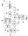
- FIG. 1 the same numerals designate the same or corresponding components as those in FIG. 7.
- the numeral 30 designates a band-pass-filter for shutting out signals over 50 MHz in the output signal line of the mixer 20 to eliminate local oscillating signals (50MHz - 120MHz).
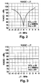
- the numeral 32 designates a first level wave-detecting circuit of this invention, having a detecting sensitivity which lowers in accordance with the detuning degree ⁇ f with respect to a predetermined central frequency e.g. IF frequency f1.
- the first level wave-detecting circuit 32 constitutes a first AGC system for applying AGC to the detected output signal level of the mixer 20 having been limited its frequency band by the band-pass-filter 30.
- the numeral 34 designates a second level wave-detecting circuit. As shown in FIG. 3, this circuit 34 has a constant detecting sensitivity irrespective of the central frequency e.g. a detuning degree with respect to the tuning frequency. T he second level wave-detecting circuit 34 constitutes a second AGC system for detecting the input signal level of the mixer 20 in accordance with the detecting sensitivity.
- the frequency property of the level wave-detecting circuit 34 must have a broad band-pass property at least approximately to 110MHz. Such a frequency band is substantially the same as that of the local oscillating signals (50MHz - 120 MHz), which would cause mis-operation of the AGC 10 by a sudden invasion of of the local oscillating signal. Therefore, in this embodiment, the AGC sensitivity (detecting sensitivity) in the second level wave-detecting circuit 34 must be restricted to be lower than that in the first level wave-detecting circuit. This AGC sensitivity is set to such a value that would not cause any mis-operation and that could eliminate the intermodulation disturbance mentioned above.
- the numeral 36 designates a adding circuit for outputting AGC signal from the AGC circuit 10 by adding the first level wave-detecting signal to the second level wave-detecting signal.
- the adding circuit 36 includes a offset circuit for determining the offset amount of the AGC controlling signal output from the adding circuit 36.
- the second level wave-detecting circuit 34 outputs the second level wave-detecting signal from the input signal level of the mixer 20 in accordance with the property represented by FIG. 3.
- the first and the second level wave-detecting signals are mutually added in the adding circuit 36, and this AGC controlling signal is supplied to the attenuator 18 of the antenna circuit 14 and the RF amplifying circuit 16.
- the integral properties could be represented by FIG. 4 formed by superimposing FIG. 2 and 3.
- the second AGC system at a broad band where the detuning degree is larger than that, the second AGC system has a priority to operate, in accordance with the input signal level of the mixer 20.
- the detecting sensitivity is kept constant by the second level wave-detecting circuit 34, thereby preventing the intermodulation disturbance over a broad frequency band, and preventing the excessive suppression of the detecting sensitivity of the central frequency by an excessive AGC application.
- the undesirable influences of the local oscillating signal can be eliminated by disposing a band-pass-filter capable of shutting out signals over 50MHz, and by enhancing, at the detuning time, the constant detecting sensitivity of the second level wave-detecting circuit to be higher than that of the first level wave-detecting circuit.
- the IF section for executing FM demodulation upon receiving the output from the mixer 20 at the front end is designated by a numeral 40.
- the output of this IF section being a multi-stage limiter is taken as a narrow band signals because of having a central frequency component.
- This IF signal is supplied to the S meter 42 where the signal level of a desired channel is detected.
- the output of the S meter (signal meter) 42 is used by the other circuits of the radio receiver, in this embodiment the output of the S meter 42 is supplied to the first level wave-detecting circuit 32 for compensating the detecting sensitivity in accordance with the output level of the IF section.
- FIG. 5 shows an AGC compensating operation of the first AGC system by the output of the IF section.
- the detecting sensitivity is controlled as shown by section lines from the state of the dashed line to the state of the solid line in accordance with the output level of the IF section.
- the chain line in FIG. 5 stands for a detecting sensitivity for the second AGC system in substantially same manner as in FIG. 4, in the case where the output of the IF section is sufficiently large.
- the solid line in FIG. 5 stands for a state where the output level of the IF section is lowered.
- the lowered control by the first AGC system acts to certainly prevent the excessive AGC application by the conventional keyed AGC, mentioned above.
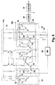
- FIG. 6 shows a more detailed AGC circuit diagram according to this invention, where the same components as in FIG. 1 are designated by the same numerals and omitted to be mentioned.
- the band-pass-filter 30, for supplying the output signal of the mixer 20 to the first level wave-detecting circuit 32 by limiting the frequency band is composed e.g. of a ceramic filter, which is represented equivalently by a resistor and a condenser.
- the shown band-pass-filter 30 can be installed separately from the ceramic filter as a two-staged filter.
- the AGC circuit being composed of IC and having the band-pass-filter therein, a stray capacitance (parasitic capacitance) would arise as shown in dashed line.
- the frequency of the band-pass-filter 30 is determined taking account of the parasitic capacitance.
- the output of the band-pass-filter 30 is supplied to the base of the transistor 50 in the first level wave-detecting circuit 32, and the signals according to the property shown in FIG. 2 are supplied to the first input transistor 52 in the adder circuit 36.
- the condenser 53 keeps the potential according to the current flowing through the transistor 50 at its upstream side, thereby currents according to the level of the input signal to the first level circuit 34 flow through the transistor 52.
- the input signal level of the mixer 20 is supplied to the base of the transistor 54 provided in the second level wave-detecting circuit 34, the output of which is supplied to the base of the second input transistor 56 in the adder circuit 36 as shown in FIG. 3.
- the condenser 55 keeps the potential according to the current flowing through the transistor 54 at its upstream side, thereby current according to the level of the input signal to the second level circuit 34 flows through the transistor 56.
- the adder circuit 36 receives an input made by mutually adding the both collector currents of the transistors 52, 56, thereby a synthesized AGC controlling signal is supplied from the output terminal 36a to the attenuator 18 and the RF amplifier 16 shown in FIG. 7 to perform the gain control.
- the adder circuit 36 contains an offset circuit therein.
- the both level wave-detecting circuits 32, 34 are provided with basic power source circuits 60, 62 respectively to supply predetermined collector currents to the transistors 50, 54 respectively.
- an AGC compensating signal is supplied from the S meter 42 to the first level wave-detecting circuit 32 in accordance with the output level of the IF section, as mentioned above.
- the output of the S meter 42 is supplied to the level converting circuit 64, the output of which is then supplied from the transistor 66 to the basic power source circuit 60 of the first level wave-detecting circuit 32.
- the detecting sensitivity of the first level wave-detecting circuit 32 can be compensated by the output of the IF output level, namely, the output of the S meter 42.
Landscapes
- Engineering & Computer Science (AREA)
- Computer Networks & Wireless Communication (AREA)
- Signal Processing (AREA)
- Control Of Amplification And Gain Control (AREA)
- Circuits Of Receivers In General (AREA)
Claims (6)
- AGC-Schaltung für einen Radioempfänger, die einen Empfangssignalpegel detektiert, um AGC-Signale entsprechend dem detektierten Signalpegel zu erzeugen, und welche die Verstärkung einer Radiofrequenzverstärkerschaltung (16) steuert, mit:a) einer Filterschaltung (30), um Komponenten eines vorbestimmten Frequenzbandes im Ausgangssignal von einem Mixer (20) durchzulassen;b) einem ersten Pegeldetektorschaltkreis (32), der eine erste AGC-Schleife bildet;c) einem zweiten Pegeldetektorschaltkreis (34) zum Detektieren eines Eingangssignals des Mixers (20) und zum Bilden einer zweiten AGC-Schleife, die eine konstante Detektionsempfindlichkeit hat, unabhängig vom Grad der Verstimmung bezüglich einer Zwischenfrequenz;d) einer Addierschaltung (36) zum Addieren des ersten Pegeldetektionssignals zum zweiten Pegeldetektionssignal, um ein AGC-Signal auszugeben;dadurch gekennzeichnet, daße) der erste Pegeldetektionsschaltkreis (32) ein Frequenzband hat, das beschränkt ist durch die Filterschaltung (30) und den Ausgangssignalpegel des Mixers (20) detektiert,f) daß die zweite AGC-Schleife eine Detektierempfindlichkeit hat, die in Abhängigkeit mit dem Grad der Verstimmung bezüglich der Zwischenfrequenz variiert,g) daß ein Signalmesser (42) den Signalpegel eines gewünschten Kanalsignalausgangs vom Zwischenfrequenzabschnitt (40) detektiert, zu welchem der Mixerausgang zugeführt wird;h) und daß ein AGC-Kompensationsschaltkreis (64) das Ausgangssignal des ersten Pegeldetektionsschaltkreises (32) reduziert in Übereinstimmung mit der Reduktion des Zwischenfrequenzsignalpegels des gewünschten Kanals, welche durch den Signalmesser (42) detektiert wird, wodurch die Detektionsempfindlichkeit der ersten AGC-Schleife abgesenkt wird, um Nachbarkanalstörungen zu reduzieren.
- AGC-Schaltung nach Anspruch 1,
wobei die Detektionsempfindlichkeit bei der zentralen Frequenz des ersten Pegeldetektionsschaltkreises (32) auf einen Wert gesetzt wird, der höher ist als der des zweiten Pegeldetektionsschaltkreises (34). - AGC-Schaltung nach Anspruch 1,
wobei der erste (32) und zweite (34) Pegeldetektionsschaltkreis jeweils aufweist:
einen Transistor (50, 54) durch welchen ein elektrischer Strom fließt in Übereinstimmung mit dem Eingangssignalpegel; einem Kondensator (53, 55), der stromab von dem Transistor angeordnet ist, um das Potential zu halten in Übereinstimmung mit dem Stromfluß durch den Transistor. - AGC-Schaltung nach Anspruch 3,
wobei der Addierschaltkreis (36) ein Paar von Transistoren (52, 56) aufweist, deren Stromfluß bestimmt ist in Übereinstimmung mit dem Stromlaufpotential des Kondensators des ersten und zweiten Pegeldetektionsschaltkreises, und daß stromauf von dem Paar von Transistoren gekuppelt ist, um einen zusätzlichen Strom hindurchzuführen. - AGC-Schaltung nach Anspruch 1,
wobei der erste Pegeldetektionsschaltkreis (32) ferner aufweist: einen Transistor (50), durch welchen ein elektrischer Strom fließt in Übereinstimmung mit dem Eingangssignalpegel;
einen Kondensator (53), der stromab vom Transistor angeordnet ist, um das Potential beizubehalten in Übereinstimmung mit dem Stromfluß des Transistors; und
eine Grundspannungsversorgungsschaltung (60) zum Aufrechterhalten des Stromflusses durch den Transistor (50). - AGC-Schaltung nach Anspruch 5,
wobei die AGC-Kompensationsschaltung (64) einen Kompensationstransistor aufweist, dessen Stromdurchfluß bestimmt wird in Übereinstimmung mit dem Ausgangssignal des Signalmessers (42); und
die Ausgangsspannung der Bezugsspannungsquelle geändert wird in Übereinstimmung mit dem Stromwert des Kompensationstransistors.
Applications Claiming Priority (4)
| Application Number | Priority Date | Filing Date | Title |
|---|---|---|---|
| JP171851/90 | 1990-06-29 | ||
| JP2171851A JP2589203B2 (ja) | 1990-06-29 | 1990-06-29 | Agc回路 |
| JP295023/90 | 1990-10-31 | ||
| JP2295023A JP2994727B2 (ja) | 1990-10-31 | 1990-10-31 | ラジオ受信機のagc回路 |
Publications (3)
| Publication Number | Publication Date |
|---|---|
| EP0464669A2 EP0464669A2 (de) | 1992-01-08 |
| EP0464669A3 EP0464669A3 (en) | 1992-01-22 |
| EP0464669B1 true EP0464669B1 (de) | 1997-06-04 |
Family
ID=26494429
Family Applications (1)
| Application Number | Title | Priority Date | Filing Date |
|---|---|---|---|
| EP91110655A Expired - Lifetime EP0464669B1 (de) | 1990-06-29 | 1991-06-27 | Automatische Verstärkungsregelung für einen Radioempfänger |
Country Status (4)
| Country | Link |
|---|---|
| US (1) | US5339453A (de) |
| EP (1) | EP0464669B1 (de) |
| KR (1) | KR0156937B1 (de) |
| DE (1) | DE69126373T2 (de) |
Families Citing this family (16)
| Publication number | Priority date | Publication date | Assignee | Title |
|---|---|---|---|---|
| AU769645B2 (en) * | 1987-05-29 | 2004-01-29 | Abbott Laboratories | Nourishing products enriched with nucleosides and/or nucleotides for infants and adults and processes for their preparation |
| JP2577490B2 (ja) * | 1990-07-03 | 1997-01-29 | 株式会社東芝 | Fmフロントエンド部のagc回路 |
| US5465406A (en) * | 1994-09-06 | 1995-11-07 | Ford Motor Company | Automatic gain control overshoot limiter for AM receiver |
| US5722063A (en) * | 1994-12-16 | 1998-02-24 | Qualcomm Incorporated | Method and apparatus for increasing receiver immunity to interference |
| DE69731137T2 (de) * | 1996-03-27 | 2006-03-09 | Philips Intellectual Property & Standards Gmbh | Verbesserung in oder bezüglich Radioempfänger |
| JPH10276112A (ja) * | 1997-03-28 | 1998-10-13 | Sanyo Electric Co Ltd | ラジオ受信機 |
| JP3203202B2 (ja) * | 1997-03-31 | 2001-08-27 | 三洋電機株式会社 | ラジオ受信機 |
| US6229998B1 (en) | 1999-04-12 | 2001-05-08 | Qualcomm Inc. | Method and system for detecting in-band jammers in a spread spectrum wireless base station |
| DE60115157T2 (de) * | 2000-07-12 | 2006-08-10 | Motorola, Inc., Schaumburg | Automatische Verstärkungsschleife mit kurzer Ansprechzeit für schmalbandige Systeme |
| US20030232613A1 (en) * | 2001-01-12 | 2003-12-18 | Kerth Donald A. | Quadrature signal generation in radio-frequency apparatus and associated methods |
| US7319884B2 (en) * | 2003-12-02 | 2008-01-15 | Matsushita Electric Industrial Co., Ltd. | FM radio device and transmission power control method |
| EP1710920A1 (de) * | 2005-04-06 | 2006-10-11 | Telefonaktiebolaget LM Ericsson (publ) | Empfang von modulierten Funksignalen |
| JP2007281939A (ja) * | 2006-04-07 | 2007-10-25 | Matsushita Electric Ind Co Ltd | 受信装置 |
| KR101014041B1 (ko) * | 2009-06-03 | 2011-02-14 | 주식회사 현대오토넷 | 주파수의 자동 선국 방법 |
| EP2296285A1 (de) * | 2009-09-14 | 2011-03-16 | Alcatel Lucent | Vorrichtung zur Verarbeitung von in Bezug auf den Frequenzbereich eingeschränkten Radiofrequenzsignalen, entsprechendes System und Verfahren |
| KR102494784B1 (ko) | 2015-07-28 | 2023-02-01 | 삼성전자주식회사 | 수신기 및 그 동작 방법 |
Family Cites Families (3)
| Publication number | Priority date | Publication date | Assignee | Title |
|---|---|---|---|---|
| US4455681A (en) * | 1981-12-21 | 1984-06-19 | Wile Donald T | Dual threshold wide band/narrow band AGC |
| DE3210454A1 (de) * | 1982-03-22 | 1983-09-22 | Licentia Patent-Verwaltungs-Gmbh, 6000 Frankfurt | Empfaenger-eingangsschaltung |
| JPS6150354U (de) * | 1984-09-03 | 1986-04-04 |
-
1991
- 1991-06-27 EP EP91110655A patent/EP0464669B1/de not_active Expired - Lifetime
- 1991-06-27 DE DE69126373T patent/DE69126373T2/de not_active Expired - Fee Related
- 1991-06-28 KR KR1019910010924A patent/KR0156937B1/ko not_active Expired - Fee Related
- 1991-06-28 US US07/723,077 patent/US5339453A/en not_active Expired - Lifetime
Non-Patent Citations (1)
| Title |
|---|
| technical papers ICCE; 08-10 June 1988 Rosemont (USA); published by IEEE, New York (USA) pg 270-271 S. Sugayama e.a. "Development of one-chip IC for car tuners". * |
Also Published As
| Publication number | Publication date |
|---|---|
| US5339453A (en) | 1994-08-16 |
| DE69126373D1 (de) | 1997-07-10 |
| KR0156937B1 (ko) | 1998-11-16 |
| KR920001867A (ko) | 1992-01-30 |
| EP0464669A2 (de) | 1992-01-08 |
| DE69126373T2 (de) | 1998-01-15 |
| EP0464669A3 (en) | 1992-01-22 |
Similar Documents
| Publication | Publication Date | Title |
|---|---|---|
| US5339453A (en) | AGC circuit for radio receiver having AGC sensitivity compensated by if output signal | |
| EP0464792B1 (de) | AGC-Schaltung einer FM-Eingangsstufe | |
| US6389272B1 (en) | Receiver with auto gain control circuit of RF signal | |
| JPH0461531B2 (de) | ||
| US3942120A (en) | SWD FM receiver circuit | |
| US4189679A (en) | Noise detecting circuit having noise-immune AGC | |
| US5732329A (en) | Radio transmitter/receiver | |
| JP2994727B2 (ja) | ラジオ受信機のagc回路 | |
| KR100420092B1 (ko) | 라디오수신기 | |
| EP1177621B1 (de) | Mos-verstärker mit variabler verstärkung | |
| JPH05300043A (ja) | アッテネータ回路 | |
| US6157269A (en) | Local oscillator noise rejection circuit | |
| US20040176060A1 (en) | High frequency device | |
| KR0177676B1 (ko) | 자동이득 제어 지연점 조정회로 | |
| US4306306A (en) | Amplitude tilt and notch compensation apparatus | |
| US7209188B2 (en) | Intermediate-frequency circuit having flat group delay characteristic | |
| US4271533A (en) | AFC Interface circuit | |
| KR0154598B1 (ko) | 튜너의 강입력보강회로 | |
| JPH0155790B2 (de) | ||
| JPH0337771B2 (de) | ||
| JP2589203B2 (ja) | Agc回路 | |
| JP2002246858A (ja) | 利得制御増幅回路およびそれを用いた受信機、送信機 | |
| JP2505500Y2 (ja) | 無線受信機 | |
| JP2003078370A (ja) | 利得可変増幅回路およびそれを用いた受信機ならびに送信機 | |
| JP2002335125A (ja) | 電圧制御発振器及びそれを用いた通信機 |
Legal Events
| Date | Code | Title | Description |
|---|---|---|---|
| PUAI | Public reference made under article 153(3) epc to a published international application that has entered the european phase |
Free format text: ORIGINAL CODE: 0009012 |
|
| PUAL | Search report despatched |
Free format text: ORIGINAL CODE: 0009013 |
|
| AK | Designated contracting states |
Kind code of ref document: A2 Designated state(s): DE FR GB |
|
| AK | Designated contracting states |
Kind code of ref document: A3 Designated state(s): DE FR GB |
|
| 17P | Request for examination filed |
Effective date: 19920305 |
|
| 17Q | First examination report despatched |
Effective date: 19940729 |
|
| GRAG | Despatch of communication of intention to grant |
Free format text: ORIGINAL CODE: EPIDOS AGRA |
|
| GRAH | Despatch of communication of intention to grant a patent |
Free format text: ORIGINAL CODE: EPIDOS IGRA |
|
| GRAH | Despatch of communication of intention to grant a patent |
Free format text: ORIGINAL CODE: EPIDOS IGRA |
|
| GRAA | (expected) grant |
Free format text: ORIGINAL CODE: 0009210 |
|
| AK | Designated contracting states |
Kind code of ref document: B1 Designated state(s): DE FR GB |
|
| REF | Corresponds to: |
Ref document number: 69126373 Country of ref document: DE Date of ref document: 19970710 |
|
| ET | Fr: translation filed | ||
| PLBE | No opposition filed within time limit |
Free format text: ORIGINAL CODE: 0009261 |
|
| STAA | Information on the status of an ep patent application or granted ep patent |
Free format text: STATUS: NO OPPOSITION FILED WITHIN TIME LIMIT |
|
| 26N | No opposition filed | ||
| REG | Reference to a national code |
Ref country code: GB Ref legal event code: IF02 |
|
| PGFP | Annual fee paid to national office [announced via postgrant information from national office to epo] |
Ref country code: FR Payment date: 20090618 Year of fee payment: 19 |
|
| PGFP | Annual fee paid to national office [announced via postgrant information from national office to epo] |
Ref country code: DE Payment date: 20090821 Year of fee payment: 19 Ref country code: GB Payment date: 20090623 Year of fee payment: 19 |
|
| GBPC | Gb: european patent ceased through non-payment of renewal fee |
Effective date: 20100627 |
|
| REG | Reference to a national code |
Ref country code: FR Ref legal event code: ST Effective date: 20110228 |
|
| PG25 | Lapsed in a contracting state [announced via postgrant information from national office to epo] |
Ref country code: DE Free format text: LAPSE BECAUSE OF NON-PAYMENT OF DUE FEES Effective date: 20110101 |
|
| PG25 | Lapsed in a contracting state [announced via postgrant information from national office to epo] |
Ref country code: FR Free format text: LAPSE BECAUSE OF NON-PAYMENT OF DUE FEES Effective date: 20100630 |
|
| PG25 | Lapsed in a contracting state [announced via postgrant information from national office to epo] |
Ref country code: GB Free format text: LAPSE BECAUSE OF NON-PAYMENT OF DUE FEES Effective date: 20100627 |