EP0465195A2 - Mehrschichtverbindungsverfahren hoher Dichte und Struktur mit thermoplastischen Klebern mit aufeinanderfolgenden abnehmenden Tg's - Google Patents
Mehrschichtverbindungsverfahren hoher Dichte und Struktur mit thermoplastischen Klebern mit aufeinanderfolgenden abnehmenden Tg's Download PDFInfo
- Publication number
- EP0465195A2 EP0465195A2 EP91305960A EP91305960A EP0465195A2 EP 0465195 A2 EP0465195 A2 EP 0465195A2 EP 91305960 A EP91305960 A EP 91305960A EP 91305960 A EP91305960 A EP 91305960A EP 0465195 A2 EP0465195 A2 EP 0465195A2
- Authority
- EP
- European Patent Office
- Prior art keywords
- layer
- high density
- density interconnect
- interconnect structure
- dielectric material
- Prior art date
- Legal status (The legal status is an assumption and is not a legal conclusion. Google has not performed a legal analysis and makes no representation as to the accuracy of the status listed.)
- Withdrawn
Links
Images

Classifications
-
- H—ELECTRICITY
- H10—SEMICONDUCTOR DEVICES; ELECTRIC SOLID-STATE DEVICES NOT OTHERWISE PROVIDED FOR
- H10W—GENERIC PACKAGES, INTERCONNECTIONS, CONNECTORS OR OTHER CONSTRUCTIONAL DETAILS OF DEVICES COVERED BY CLASS H10
- H10W70/00—Package substrates; Interposers; Redistribution layers [RDL]
- H10W70/60—Insulating or insulated package substrates; Interposers; Redistribution layers
- H10W70/611—Insulating or insulated package substrates; Interposers; Redistribution layers for connecting multiple chips together
- H10W70/614—Insulating or insulated package substrates; Interposers; Redistribution layers for connecting multiple chips together the multiple chips being integrally enclosed
-
- H—ELECTRICITY
- H05—ELECTRIC TECHNIQUES NOT OTHERWISE PROVIDED FOR
- H05K—PRINTED CIRCUITS; CASINGS OR CONSTRUCTIONAL DETAILS OF ELECTRIC APPARATUS; MANUFACTURE OF ASSEMBLAGES OF ELECTRICAL COMPONENTS
- H05K3/00—Apparatus or processes for manufacturing printed circuits
- H05K3/46—Manufacturing multilayer circuits
- H05K3/4611—Manufacturing multilayer circuits by laminating two or more circuit boards
- H05K3/4626—Manufacturing multilayer circuits by laminating two or more circuit boards characterised by the insulating layers or materials
- H05K3/4635—Manufacturing multilayer circuits by laminating two or more circuit boards characterised by the insulating layers or materials laminating flexible circuit boards using additional insulating adhesive materials between the boards
-
- H—ELECTRICITY
- H05—ELECTRIC TECHNIQUES NOT OTHERWISE PROVIDED FOR
- H05K—PRINTED CIRCUITS; CASINGS OR CONSTRUCTIONAL DETAILS OF ELECTRIC APPARATUS; MANUFACTURE OF ASSEMBLAGES OF ELECTRICAL COMPONENTS
- H05K3/00—Apparatus or processes for manufacturing printed circuits
- H05K3/46—Manufacturing multilayer circuits
- H05K3/4644—Manufacturing multilayer circuits by building the multilayer layer by layer, i.e. build-up multilayer circuits
- H05K3/4673—Application methods or materials of intermediate insulating layers not specially adapted to any one of the previous methods of adding a circuit layer
-
- H—ELECTRICITY
- H10—SEMICONDUCTOR DEVICES; ELECTRIC SOLID-STATE DEVICES NOT OTHERWISE PROVIDED FOR
- H10W—GENERIC PACKAGES, INTERCONNECTIONS, CONNECTORS OR OTHER CONSTRUCTIONAL DETAILS OF DEVICES COVERED BY CLASS H10
- H10W70/00—Package substrates; Interposers; Redistribution layers [RDL]
- H10W70/60—Insulating or insulated package substrates; Interposers; Redistribution layers
- H10W70/67—Insulating or insulated package substrates; Interposers; Redistribution layers characterised by their insulating layers or insulating parts
- H10W70/68—Shapes or dispositions thereof
- H10W70/685—Shapes or dispositions thereof comprising multiple insulating layers
-
- H—ELECTRICITY
- H05—ELECTRIC TECHNIQUES NOT OTHERWISE PROVIDED FOR
- H05K—PRINTED CIRCUITS; CASINGS OR CONSTRUCTIONAL DETAILS OF ELECTRIC APPARATUS; MANUFACTURE OF ASSEMBLAGES OF ELECTRICAL COMPONENTS
- H05K1/00—Printed circuits
- H05K1/18—Printed circuits structurally associated with non-printed electric components
- H05K1/182—Printed circuits structurally associated with non-printed electric components associated with components mounted in printed circuit boards [PCB], e.g. insert-mounted components [IMC]
- H05K1/185—Printed circuits structurally associated with non-printed electric components associated with components mounted in printed circuit boards [PCB], e.g. insert-mounted components [IMC] associated with components encapsulated in the insulating substrate of the PCBs; associated with components incorporated in internal layers of multilayer circuit boards
-
- H—ELECTRICITY
- H05—ELECTRIC TECHNIQUES NOT OTHERWISE PROVIDED FOR
- H05K—PRINTED CIRCUITS; CASINGS OR CONSTRUCTIONAL DETAILS OF ELECTRIC APPARATUS; MANUFACTURE OF ASSEMBLAGES OF ELECTRICAL COMPONENTS
- H05K2201/00—Indexing scheme relating to printed circuits covered by H05K1/00
- H05K2201/01—Dielectrics
- H05K2201/0104—Properties and characteristics in general
- H05K2201/0129—Thermoplastic polymer, e.g. auto-adhesive layer; Shaping of thermoplastic polymer
-
- H—ELECTRICITY
- H05—ELECTRIC TECHNIQUES NOT OTHERWISE PROVIDED FOR
- H05K—PRINTED CIRCUITS; CASINGS OR CONSTRUCTIONAL DETAILS OF ELECTRIC APPARATUS; MANUFACTURE OF ASSEMBLAGES OF ELECTRICAL COMPONENTS
- H05K2201/00—Indexing scheme relating to printed circuits covered by H05K1/00
- H05K2201/01—Dielectrics
- H05K2201/0137—Materials
- H05K2201/0154—Polyimide
-
- H—ELECTRICITY
- H05—ELECTRIC TECHNIQUES NOT OTHERWISE PROVIDED FOR
- H05K—PRINTED CIRCUITS; CASINGS OR CONSTRUCTIONAL DETAILS OF ELECTRIC APPARATUS; MANUFACTURE OF ASSEMBLAGES OF ELECTRICAL COMPONENTS
- H05K2201/00—Indexing scheme relating to printed circuits covered by H05K1/00
- H05K2201/01—Dielectrics
- H05K2201/0183—Dielectric layers
- H05K2201/0195—Dielectric or adhesive layers comprising a plurality of layers, e.g. in a multilayer structure
-
- H—ELECTRICITY
- H05—ELECTRIC TECHNIQUES NOT OTHERWISE PROVIDED FOR
- H05K—PRINTED CIRCUITS; CASINGS OR CONSTRUCTIONAL DETAILS OF ELECTRIC APPARATUS; MANUFACTURE OF ASSEMBLAGES OF ELECTRICAL COMPONENTS
- H05K3/00—Apparatus or processes for manufacturing printed circuits
- H05K3/38—Improvement of the adhesion between the insulating substrate and the metal
- H05K3/386—Improvement of the adhesion between the insulating substrate and the metal by the use of an organic polymeric bonding layer, e.g. adhesive
-
- H—ELECTRICITY
- H05—ELECTRIC TECHNIQUES NOT OTHERWISE PROVIDED FOR
- H05K—PRINTED CIRCUITS; CASINGS OR CONSTRUCTIONAL DETAILS OF ELECTRIC APPARATUS; MANUFACTURE OF ASSEMBLAGES OF ELECTRICAL COMPONENTS
- H05K3/00—Apparatus or processes for manufacturing printed circuits
- H05K3/46—Manufacturing multilayer circuits
- H05K3/4644—Manufacturing multilayer circuits by building the multilayer layer by layer, i.e. build-up multilayer circuits
-
- H—ELECTRICITY
- H10—SEMICONDUCTOR DEVICES; ELECTRIC SOLID-STATE DEVICES NOT OTHERWISE PROVIDED FOR
- H10W—GENERIC PACKAGES, INTERCONNECTIONS, CONNECTORS OR OTHER CONSTRUCTIONAL DETAILS OF DEVICES COVERED BY CLASS H10
- H10W70/00—Package substrates; Interposers; Redistribution layers [RDL]
- H10W70/01—Manufacture or treatment
- H10W70/05—Manufacture or treatment of insulating or insulated package substrates, or of interposers, or of redistribution layers
- H10W70/093—Connecting or disconnecting other interconnections thereto or therefrom, e.g. connecting bond wires or bumps
-
- H—ELECTRICITY
- H10—SEMICONDUCTOR DEVICES; ELECTRIC SOLID-STATE DEVICES NOT OTHERWISE PROVIDED FOR
- H10W—GENERIC PACKAGES, INTERCONNECTIONS, CONNECTORS OR OTHER CONSTRUCTIONAL DETAILS OF DEVICES COVERED BY CLASS H10
- H10W70/00—Package substrates; Interposers; Redistribution layers [RDL]
- H10W70/099—Connecting interconnections to insulating or insulated package substrates, interposers or redistribution layers
-
- H—ELECTRICITY
- H10—SEMICONDUCTOR DEVICES; ELECTRIC SOLID-STATE DEVICES NOT OTHERWISE PROVIDED FOR
- H10W—GENERIC PACKAGES, INTERCONNECTIONS, CONNECTORS OR OTHER CONSTRUCTIONAL DETAILS OF DEVICES COVERED BY CLASS H10
- H10W70/00—Package substrates; Interposers; Redistribution layers [RDL]
- H10W70/60—Insulating or insulated package substrates; Interposers; Redistribution layers
- H10W70/67—Insulating or insulated package substrates; Interposers; Redistribution layers characterised by their insulating layers or insulating parts
- H10W70/68—Shapes or dispositions thereof
- H10W70/682—Shapes or dispositions thereof comprising holes having chips therein
-
- H—ELECTRICITY
- H10—SEMICONDUCTOR DEVICES; ELECTRIC SOLID-STATE DEVICES NOT OTHERWISE PROVIDED FOR
- H10W—GENERIC PACKAGES, INTERCONNECTIONS, CONNECTORS OR OTHER CONSTRUCTIONAL DETAILS OF DEVICES COVERED BY CLASS H10
- H10W72/00—Interconnections or connectors in packages
- H10W72/071—Connecting or disconnecting
- H10W72/073—Connecting or disconnecting of die-attach connectors
-
- H—ELECTRICITY
- H10—SEMICONDUCTOR DEVICES; ELECTRIC SOLID-STATE DEVICES NOT OTHERWISE PROVIDED FOR
- H10W—GENERIC PACKAGES, INTERCONNECTIONS, CONNECTORS OR OTHER CONSTRUCTIONAL DETAILS OF DEVICES COVERED BY CLASS H10
- H10W72/00—Interconnections or connectors in packages
- H10W72/851—Dispositions of multiple connectors or interconnections
- H10W72/874—On different surfaces
-
- H—ELECTRICITY
- H10—SEMICONDUCTOR DEVICES; ELECTRIC SOLID-STATE DEVICES NOT OTHERWISE PROVIDED FOR
- H10W—GENERIC PACKAGES, INTERCONNECTIONS, CONNECTORS OR OTHER CONSTRUCTIONAL DETAILS OF DEVICES COVERED BY CLASS H10
- H10W90/00—Package configurations
Definitions
- the present invention relates to the field of high density interconnect structures for interconnecting electronic components, and more particularly, to such structures employing more than one layer of conductors.
- a high density interconnect (HDI) structure or system which has been developed by General Electric Company offers many advantages in the compact assembly of electronic systems.
- an electronic system such as a micro computer which incorporates 30-50 chips can be fully assembled and interconnected on a single substrate which is 2 inch long by 2 inch wide by .050 inch thick.
- this interconnect structure can be disassembled for repair or replacement of a faulty component and then reassembled without significant risk to the good components incorporated within the system. This is particularly important where as many as 50 chips having a cost of as much as $2,000.00, each, may be incorporated in a single system on one substrate.
- This repairability is a substantial advance over prior connection systems in which reworking the system to replace damaged components was either impossible or involved substantial risk to the good components.
- a ceramic substrate such as alumina which may be 100 mils thick and of appropriate size and strength for the overall system, is provided. This size is typically less than 2 inches square, but may be made larger or smaller.
- individual cavities or one large cavity having appropriate depth at the intended locations of differing chips is prepared. This may be done by starting with a bare substrate having a uniform thickness and the desired size. Conventional, ultrasonic or laser milling may be used to form the cavities in which the various chips and other components will be positioned. For many systems where it is desired to place chips nearly edge-to-edge, a single large cavity is satisfactory. That large cavity may typically have a uniform depth where the semiconductor chips have a substantially uniform thickness.
- the cavity bottom may be made respectively deeper or shallower to place the upper surface of the corresponding component in substantially the same plane as the upper surface of the rest of the components and the portion of the substrate which surrounds the cavity.
- the bottom of the cavity is then provided with a thermoplastic adhesive layer which may preferably be polyetherimide resin available under the trade name ULTEM® 6000 from the General Electric Company.
- the various components are then placed in their desired locations within the cavity, the entire structure is heated to about 300°C which is above the softening point of the ULTEM® polyetherimide (which is in the vicinity of 235°C) and then cooled to thermoplastically bond the individual components to the substrate.
- a polyimide film which may be Kapton® polyimide, available from E.I. du Pont de Nemours Company, which is ⁇ 0.0005-0.003 inch ( ⁇ 12.5-75 microns) thick is pretreated to promote adhesion by reactive ion etching (RIE), the substrate and chips are then coated with ULTEM® 1000 polyetherimide resin or another thermoplastic and the Kapton film is laminated across the top of the chips, any other components and the substrate with the ULTEM® resin serving as a thermoplastic adhesive to hold the Kapton® in place. Thereafter, via holes are provided (preferably by laser drilling) in the Kapton® and ULTEM® layers in alignment with the contact pads on the electronic components to which it is desired to make contact.
- Kapton® polyimide available from E.I. du Pont de Nemours Company
- a metallization layer which is deposited over the Kapton® layer extends into the via holes and makes electrical contact to the contact pads disposed thereunder.
- This metallization layer may be patterned to form individual conductors during the process of depositing it or may be deposited as a continuous layer and then patterned using photoresist and etching.
- the photoresist is preferably exposed using a laser to provide an accurately aligned conductor pattern at the end of the process. Alternatively, exposure through a mask may be used.
- This high density interconnect structure provides many advantages. Included among these are the lightest weight and smallest volume packaging of such an electronic system presently available. A further, and possibly more significant advantage of this high density interconnect structure, is the short time required to design and fabricate a system using this high density interconnect structure.
- Prior art processes require the prepackaging of each semiconductor chip, the design of a multilayer circuit board to interconnect the various packaged chips, and so forth. Multilayer circuit boards are expensive and require substantial lead time for their fabrication. In contrast, the only thing which must be specially pre-fabricated for the HDI system is the substrate on which the individual semiconductor chips will be mounted.
- This substrate is a standard stock item, other than the requirement that the substrate have appropriate cavities therein for the placement of the semiconductor chips so that the interconnect surface of the various chips and the substrate will be in a single plane.
- the required cavities may be formed in an already fired ceramic substrate by conventional or laser milling. This milling process is straightforward and fairly rapid with the result that once a desired configuration for the substrate has been established, a corresponding physical substrate can be made ready for the mounting of the semiconductor chips in as little as 1 day and typically 4 hours for small quantities as are suitable for research or prototype systems to confirm the design prior to quantity production.
- the process of designing an interconnection pattern for interconnecting all of the chips and components of an electronic system on a single high density interconnect substrate normally takes somewhere between one week and five weeks. Once that interconnect structure has been defined, assembly of the system on the substrate may begin. First, the chips are mounted on the substrate and the overlay structure is built-up on top of the chips and substrate, one layer at a time. Typically, the entire process can be finished in one day and in the event of a high priority rush, could be completed in four hours. Consequently, this high density interconnect structure not only results in a substantially lighter weight and more compact package for an electronic system, but enables a prototype of the system to be fabricated and tested in a much shorter time than is required with other packaging techniques.
- any additional dielectric layers which are required for isolation between the first metallization layer and any subsequent metallization layers or for prevention of short circuits due to contact with external conductors are formed by spinning on or spraying on a solvent solution of a desired thermoplastic dielectric material. The structure is then baked to drive off the solvent in order to leave a solvent-free dielectric layer.
- a siloxane-polyimide/epoxy blend may be spun-on, dried and cured to provide this dielectric layer.
- thermoplastic polymer material we mean a polymer material which after multiple cycles of heating and cooling substantially retains its initial melting point or glass transition temperature. That is, no substantial crosslinking of the material takes place during the heating, melting and resolidification process.
- Such polymers are suitable as adhesive layers for bonding higher temperature materials, including polymers to substrates and may also themselves be used as layers to be bonded to substrates through the use of lower temperature adhesive layers.
- the glass transition temperature of a polymer is the temperature above which the viscosity of the polymer decreases greatly, thereby allowing the polymer to flow and also to bond to other materials. When cooled below this glass transition temperature, the thermoplastic polymer "resolidifies" and remains adherent to objects with which it is in intimate contact.
- thermoset polymer material we mean a polymer material in which cross-linking takes place the first time it is heated or during its preparation process, such that the material either no longer melts or melts at a much higher temperature than it did prior to its initial heating or its formation, as the case may be.
- thermoset materials as adhesives in the formation of multilayer printed circuit boards. These include spinning on a precursor of a thermoset material and reacting it in place to form a thermoset dielectric layer. Once such a layer has reacted, it is no longer soluble in the solvent which is used in forming the next layer with the result that damage to underlying layers does not occur during the formation of subsequent layers. Such materials are available from Sheldahl Corporation.
- thermoset technique is the type of laminate used in making laminated circuit boards. These include the copper dielectric laminate available under the trademark Pyrolux® from Dupont. These systems use acrylate adhesives which become thermoset at a curing temperature of about 135°C Unfortunately, acrylate adhesives are not considered sufficiently thermally stable for use in most high density interconnect structures of the type to which the present invention is directed and once reacted generally don't solvent at all. In particular, it is considered desirable to be able to operate these high density interconnect structure systems in the vicinity of 200°C or higher. Acrylates are not considered usable above 150°C. Epoxies also exhibit thermal instabilities which prevent their use at these temperatures. In particular, most epoxies turn tan at 150°C and turn black at 180°C.
- thermoset structure While use of a thermoset structure is beneficial in the printed circuit board art, the use of such thermoset systems is unacceptable in a high density interconnect structure of the type to which this invention is directed because the expensive chips are put in place before the interconnection structure is built. As a result, any fault in a thermoset high density interconnect structure would require scrapping not only of the interconnection structure itself, but all of the chips as well. Thus, the conversion of a high density interconnect structure of the type described above into one having a thermoset structure is not a solution to the problems associated with the formation of multilayered high density interconnect structures
- thermoset dielectric layers which are laminated to the structure using a thermoplastic adhesive to provide such a multilayer structure in which each dielectric layer includes a thermoset upper sublayer and a thermoplastic lower sublayer as discussed in U.S. Patent 4,783,695 has not been implemented because of the tendency for the early laminated layers to shift, deform or otherwise change during the lamination of subsequent layers in a way which breaks via connections between layers.
- a primary object of the present invention is to provide upper layer dielectrics in a high density interconnect structure by a process which avoids solvent deposition and baking of those dielectric layers.
- Another object of the present invention is to provide a planar multi-laminated high density interconnect structure whose fabrication avoids the problem of via interconnection destruction during fabrication.
- Another object of the present invention is to provide a planar multi-laminated high density interconnect structure which is laminated using progressively lower T g thermoplastic adhesives.
- Another object of the present invention is to provide greater versatility and variety in high density interconnect structures, the materials of which they are fabricated and the process of fabricating them.
- Another object of the present invention is to provide repair for each laminated layer in a high density interconnect structure without the need for total dielectric and interconnect removal.
- a high density interconnect structure is fabricated by laminating a first dielectric film over the electronic components using a first thermoplastic adhesive having a first glass transition temperature (T g1 ), forming via holes in that dielectric layer in alignment with the contact pads to which contact is to be made, forming a patterned metallization layer on top of that first dielectric layer, laminating a second dielectric film over the first metallization layer and the exposed portions of the first dielectric layer by employing a second thermoplastic adhesive having a second glass transition temperature T g2 which is lower than T g1 .
- T g1 first glass transition temperature
- This second lamination step is carried out at a temperature which is low enough that via connections between the first metallization layer and contact pads on the electronic components are neither destroyed nor otherwise adversely affected.
- via holes are formed in the second dielectric layer in alignment with conductors to which it is desired to form electrical contacts. These conductors may be conductors of the first metallization layer or contact pads of the electronic components.
- a second metallization layer is then formed over the second dielectric layer and patterned appropriately. If more conductive layers are required, additional dielectric films may be laminated to the structure with still lower T g adhesives and appropriate conductive layers may be formed thereover.
- FIG. 1 a small portion 100 of a prior art high density interconnect structure which includes a first level via connection is illustrated in cross-section.
- This high density interconnect structure includes a laminated first dielectric layer 122 and a spun-on second dielectric layer 132.
- This structure comprises a chip 116 having a contact pad 118 on its upper surface.
- a first layer 120 of the overlying high density interconnect structure comprises a dielectric layer 122 and a patterned metallization layer 128.
- the dielectric layer 122 has separate lower and upper sublayers 124 and 126, respectively.
- the sublayer 124 is a thermoplastic adhesive such as ULTEM® 1000 polyetherimide resin available from General Electric Company and the sublayer 126 is a Kapton® polyimide thermoset film, available from E.I.
- a second layer 130 of the high density interconnect structure is disposed on layer 120 and comprises a dielectric layer 132 and a patterned metallization layer 138.
- the dielectric layer 132 is a spun-on thermoplastic layer such as SPI siloxane polyimide available from HULS America.
- each dielectric layer consisted of a thermoplastic lower layer and a thermoset upper layer and in which via connections were destroyed during the process of laminating subsequent dielectric layer.
- FIG. 2 illustrates a small portion of such a cross-section.
- the cross-sectioned high density interconnect structure 200 includes laminated first and second dielectric layers 222 and 232, respectively. This structure comprises a chip 216 having a contact pad 218 on its upper surface.
- a first layer 220 of the overlying high density interconnect structure comprises a dielectric layer 222 and a patterned metallization layer 228.
- the dielectric layer 222 has separate lower and upper sublayers 224 and 226, respectively.
- the lower sublayer 224 is an ULTEM® 1000 polyetherimide resin available from General Electric Company thermoplastic adhesive and the upper sublayer 226 is a KAPTON® polyimide thermoset film available from E. I. DuPont de Nemours.
- the metallization 228 extends down into a via hole 227 and includes a portion disposed in ohmic contact with the contact pad 218.
- the upper part of the sidewalls of the via hole 227 are sloped upward and outward as a result of its formation by laser drilling.
- a second layer 230 of the high density interconnect structure is disposed on layer 220 and comprises a dielectric layer 232 and a patterned metallization layer 238.
- the dielectric layer 232 has separate lower and upper sublayers 234 and 236, respectively.
- the lower sublayer 234 is an ULTEM® 1000 polyetherimide resin available from General Electric Company thermoplastic adhesive and the upper sublayer 236 is a KAPTON® polyimide thermoset film available from E. I. DuPont de Nemours.
- the broken via shown in Figure 2 is typical of broken vias we sectioned in that the via has been expanded into the space underneath the thermoset upper sublayer 226 portion of the lower dielectric layer 222.
- the metallization of the via is typically fractured at the lower edge of the upper sublayer 226, leaving a gap 229 in metallization 228.
- This post-lamination via configuration results from the thermoplastic adhesive 234 of the second dielectric layer pushing down into the via and applying side-wise pressure which causes the second adhesive 234 to flow in under the thermoset sublayer 226 of the first dielectric layer as the adhesive 234 pushes the metallization ahead of it, in underneath that thermoset sublayer 226, with the metallization in turn pushing the adhesive sublayer 224 of the first dielectric layer ahead of it.
- thermoset adhesive printed circuit board art by the thermosetting of that first adhesive layer prior to laminating the second dielectric layer.
- a solution to this problem is performing subsequent laminations at low enough temperatures and lamination pressures that the first layer thermoplastic adhesive does not flow.
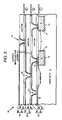
- a high density interconnect structure 10 in accordance with the present invention is illustrated in a cross-section view in Figure 3.
- the high density interconnect structure 10 comprises a substrate 12 having cavities 14 in the upper surface thereof in which integrated circuit chips 16 or other electronic components are disposed. For many high density interconnect structures, these electronic components are bonded to the substrate with a thermoplastic adhesive 15. These electronic components have contact pads 18 on an (upper) contact surface thereof.
- the substrate 12 may have conductive runs 13 disposed on the upper surface thereof.
- a first layer 20 of the overlying high density interconnect structure 10 comprises a dielectric layer 22 and a patterned metallization layer 28.
- the dielectric layer 22 has separate lower and upper sublayers 24 and 26, respectively.
- the layer 24 is a thermoplastic adhesive having a first glass transition temperature T g1 .
- the layer 26 may be a thermoset material or a thermoplastic material having a higher T g than T g1 . Where the components or chips are bonded to the substrate with a thermoplastic chip adhesive 15, it is preferred that the chip adhesive have a glass transition temperature (T g0 ) which is higher than T g1 .
- T g0 glass transition temperature
- the upper sublayer 26 of the first dielectric layer 22 should be stable over a range of temperatures above T g1 in order that it will remain stable during its lamination to the chips during the fabrication process. It is preferred that layer 26 be stable at least 100°C above T g1 . By stable, we mean it has sufficient viscosity that it doesn't shift, stretch or otherwise change in an undesirable manner during the lamination step.
- This layer 26 is preferably a thermoset film, for example, Kapton® which is sold by E.I. Dupont de Nemours. Other materials, including thermoplastics, which exhibit sufficient stability may also be used.
- the patterned metallization layer 28 extends into contact with contact pads 18 and conductor runs 13, if any, on the substrate 12 within via holes 23 in the dielectric layer 22.
- a second layer 30 of the high density interconnect structure comprises a second dielectric layer 32 and a second patterned metallization layer 38.
- the dielectric layer 32 has separate lower and upper sublayers 34 and 36, respectively.
- the second lower sublayer 34 has a second glass transition temperature T g2 and the upper sublayer 36 may again be a thermoset material or a thermoplastic material having a T g which is higher than T g2 .
- the patterned metallization 38 extends into via holes 33 in the dielectric layer 32 to make contact with the first metallization layer 28. If desired, selected via holes 33 may extend through dielectric layer 22 as well to provide direct contact to selected contact pads. However, that is not preferred because of the added processing complexity which results from having via holes of different depths.
- a third layer of the high density interconnect structure 40 comprises a dielectric layer 42 and a patterned metallization layer 48.
- the dielectric layer 42 has separate lower and upper sublayers 44 and 46.
- the third lower sublayer 44 has a glass transition temperature T g3 which is lower than T g2 .
- the third upper dielectric sublayer 46 may be a thermoset material or a thermoplastic material having a higher glass transition temperature than T g3 .
- thermoplastic adhesive materials 24, 34 and 44 are selected so that their glass transition temperatures decrease progressively. That is, T g1 > T g2 > T g3 .
- This difference in glass transition temperatures is selected in order that the second dielectric layer may be laminated onto the first layer of the high density interconnect structure at a temperature at which the first thermoplastic adhesive layer 24 is sufficiently stable that the via connections between the first metallization layer 28 and the contact pads 18 and metallization runs 13 on the substrate will not be disturbed.
- the required difference between T g1 and T g2 depends on the particular characteristics of the thermoplastic materials.
- T g 's of these materials range from greater than 300°C to the vicinity of 150°C or lower.
- the highest T g adhesive is preferably used to bond the chips to the substrate with progressively lower T g adhesives used for the laminations.
- thermoplastic adhesives having appropriately stepped T g 's is:
- thermoplastic adhesives with different T g values to obtain a desired T g and laminating temperature which is otherwise unobtainable.
- thermoplastic adhesives are commercially available and their physical properties well characterized. Potential materials for use in this invention can be found from sources such as "Plastics; Thermoplastics and Thermosets", published by The International Plastics Selector, Inc.
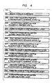
- FIG. 3 A preferred process 300 for producing the structure shown in Figure 3 is illustrated in Figure 4.
- the process 300 begins with a first step 301 of mounting the chips on the substrate 12.
- This mounting may be intended to be permanent where the substrate will remain part of the completed structure or may be intended to be temporary where the substrate will be removed following completion of the fabrication process in order to provide a flexible high density interconnect structure.
- the first upper sublayer 26 of dielectric material is coated with a thermoplastic adhesive 24.
- the thermoplastic adhesive 24 has a first glass transition temperature T g1 .
- this first dielectric layer is laminated to the chips and substrate at a first lamination temperature T1.
- step 304 the via holes 23 are formed in this first dielectric layer.
- a patterned metallization layer 28 is formed on this first dielectric layer. This may be done by any of the variety of techniques taught in the listed patents or by other patterned deposition or uniform deposition followed by patterning techniques. This completes the fabrication of the first layer 20 of the high density interconnect structure, as illustrated in Figure 3.
- the second upper sublayer 36 dielectric material is coated with a thermoplastic adhesive 34 having second glass transition temperature T g2 , which is lower than the first glass transition temperature T g1 .
- This adhesive layer should be thicker than the metallization runs it is to cover in order to avoid leaving voids in the structure adjacent those metallization runs at the completion of the laminating step.
- this second dielectric layer is laminated on top of the existing structure, that is, on top of the patterned metallization layer 28 and exposed portions of the first dielectric layer 22.
- This second lamination step is carried out at a temperature T2, which is lower than the first lamination temperature T1.
- step 308 via holes are formed in this second dielectric layer.
- a second patterned metallization layer 38 is formed on top of the second dielectric layer 32 using the same or a different metallization technique as was used for the first metallization layer, as may be desired. This completes the fabrication of the second layer 30 of a high density interconnect structure of Figure 3.
- step 310 the process continues in step 310 with coating the third upper dielectric sublayer 46 with a third thermoplastic adhesive having a third glass transition temperature T g3 which is lower than T g2 .
- this third dielectric layer is laminated to the existing structure at a temperature T3, that is, to the patterned metallization layer 38 and exposed portions of the dielectric layer 32.
- the temperature T3 is lower than the temperature T2.
- step 312 via holes 43 are formed in the third dielectric layer 42 and in step 313, a third patterned metallization layer 48 is formed on the third dielectric layer.
- the temperatures T1, T2 and T3 are selected so that T1 > T2 > T3 in order that each of the underlying layers of the high density interconnect structure will remain stable during the subsequent laminating steps.
- the required difference in temperature at successive lamination steps depends on the particular adhesives and other lamination conditions employed.
- the lamination which employs an adhesive with T g2 can be performed at a temperature above T g1 , so long as the first adhesive is sufficiently stable at that lamination temperature that no shifting or breakage of via interconnections takes place.
- the nine adhesives listed in the table, or blends prepared from these adhesives make a nine lamination structure feasible.
- most circuits, even very complex ones, can be interconnected in a structure which includes substantially fewer laminations than nine.
- lamination temperatures of BPADA/SDAN and ULTEM 6000, 310°C and 300°C, respectively and those of M&T 2065 and polyester T-230, 160°C and 150°C, respectively, are close enough together that use of both materials in each pair in the same structure should be carefully controlled or avoided.
- Each of these adhesives is either inherently laser drillable at 351 nm or may be modified to be so in accordance with application Serial No. 456,421, filed December 26, 1989, entitled “Laser Ablatable Polymer Dielectrics and Methods" by H.S. Cole et al.
- each of the adhesive layers should to remain a thermoplastic throughout the life of the structure in order to facilitate repair of the structure in the event that one of the electronic components or a portion of the interconnect structure should be found to be faulty.
- the structure can be repaired by removing the overlay structure by heating the overall structure to above the glass transition temperature of the adhesive layer 24 and then peeling the high density interconnect structure off the substrate and electronic components 16.
- the present invention provides additional versatility because by appropriately controlling the temperature to which the structure is heated, only selected layers of the high density interconnect structure need be removed where the fault is in the interconnect structure itself, rather than in one of the electronic components.
- the structure is illustrated as including a substrate 12, it should be understood that in accordance with application Serial No. 250,010, entitled, "High Density Interconnect With High Volumetric Efficiency” and application Serial No. 07/504,769, entitled, "A Flexible High Density Interconnect Structure and Flexibly Interconnected System", the substrate may be removed following fabrication of the interconnect structure to leave the electronic components 16 bonded directly to the high density interconnect structure and otherwise unsupported.
- thermoplastic adhesive may be applied on top of the high density interconnect structure prior to applying the upper sublayer either with an additional layer of that thermoplastic adhesive disposed on the upper sublayer or without further adhesive thereon.
- a final upper spun-on dielectric layer may be used, either for insulation purposes only or to support a final metallization layer. This avoids those problems with spun-on layers which arise only when a second spun-on layer is applied.
Landscapes
- Engineering & Computer Science (AREA)
- Manufacturing & Machinery (AREA)
- Microelectronics & Electronic Packaging (AREA)
- Production Of Multi-Layered Print Wiring Board (AREA)
- Laminated Bodies (AREA)
Applications Claiming Priority (2)
| Application Number | Priority Date | Filing Date | Title |
|---|---|---|---|
| US546963 | 1990-07-02 | ||
| US07/546,963 US5157589A (en) | 1990-07-02 | 1990-07-02 | Mutliple lamination high density interconnect process and structure employing thermoplastic adhesives having sequentially decreasing TG 's |
Publications (2)
| Publication Number | Publication Date |
|---|---|
| EP0465195A2 true EP0465195A2 (de) | 1992-01-08 |
| EP0465195A3 EP0465195A3 (en) | 1992-02-12 |
Family
ID=24182748
Family Applications (1)
| Application Number | Title | Priority Date | Filing Date |
|---|---|---|---|
| EP19910305960 Withdrawn EP0465195A3 (en) | 1990-07-02 | 1991-07-01 | Multiple lamination high density interconnect process and structure employing thermoplastic adhesives having sequentially decreasing tg's |
Country Status (3)
| Country | Link |
|---|---|
| US (1) | US5157589A (de) |
| EP (1) | EP0465195A3 (de) |
| JP (1) | JPH04233266A (de) |
Cited By (4)
| Publication number | Priority date | Publication date | Assignee | Title |
|---|---|---|---|---|
| US5479054A (en) * | 1992-03-17 | 1995-12-26 | Mitsubishi Denki Kabushiki Kaisha | Semiconductor device with improved planarization properties |
| US6251955B1 (en) | 1994-02-28 | 2001-06-26 | Millennium Pharmaceuticals, Inc. | Methods for identifying inhibitors of fungal pathogenicity |
| US6263563B1 (en) | 1997-11-03 | 2001-07-24 | R-Amtech International, Inc. | Method of manufacturing and checking electronic components |
| WO2004100259A3 (de) * | 2003-05-09 | 2005-03-31 | Eupec Gmbh & Co Kg | Halbleiterbauelement und verfahren zum herstellen eines halbleiterbauelements |
Families Citing this family (54)
| Publication number | Priority date | Publication date | Assignee | Title |
|---|---|---|---|---|
| JP2966972B2 (ja) * | 1991-07-05 | 1999-10-25 | 株式会社日立製作所 | 半導体チップキャリアとそれを実装したモジュール及びそれを組み込んだ電子機器 |
| JP3026465B2 (ja) * | 1992-03-10 | 2000-03-27 | 株式会社日立製作所 | セラミック薄膜混成配線基板および製造方法 |
| US5455459A (en) * | 1992-03-27 | 1995-10-03 | Martin Marietta Corporation | Reconstructable interconnect structure for electronic circuits |
| KR950012658B1 (ko) * | 1992-07-24 | 1995-10-19 | 삼성전자주식회사 | 반도체 칩 실장방법 및 기판 구조체 |
| US5306670A (en) * | 1993-02-09 | 1994-04-26 | Texas Instruments Incorporated | Multi-chip integrated circuit module and method for fabrication thereof |
| JPH07193184A (ja) * | 1993-12-27 | 1995-07-28 | Fujitsu Ltd | マルチチップモジュールの製造方法及びマルチチップモジュール |
| US5500534A (en) * | 1994-03-31 | 1996-03-19 | Iowa State University Research Foundation | Integrated energy-sensitive and position-sensitive x-ray detection system |
| US5434751A (en) * | 1994-04-11 | 1995-07-18 | Martin Marietta Corporation | Reworkable high density interconnect structure incorporating a release layer |
| US5798286A (en) | 1995-09-22 | 1998-08-25 | Tessera, Inc. | Connecting multiple microelectronic elements with lead deformation |
| US5552633A (en) * | 1995-06-06 | 1996-09-03 | Martin Marietta Corporation | Three-dimensional multimodule HDI arrays with heat spreading |
| WO1997001437A1 (en) * | 1995-06-28 | 1997-01-16 | Fraivillig Materials Company | Circuit board laminates and method of making |
| US5866952A (en) * | 1995-11-30 | 1999-02-02 | Lockheed Martin Corporation | High density interconnected circuit module with a compliant layer as part of a stress-reducing molded substrate |
| US5945203A (en) * | 1997-10-14 | 1999-08-31 | Zms Llc | Stratified composite dielectric and method of fabrication |
| US6025995A (en) * | 1997-11-05 | 2000-02-15 | Ericsson Inc. | Integrated circuit module and method |
| KR100302594B1 (ko) * | 1998-10-14 | 2001-09-22 | 김영환 | 반도체패키지용부재,반도체패키지및그제조방법 |
| US6965165B2 (en) | 1998-12-21 | 2005-11-15 | Mou-Shiung Lin | Top layers of metal for high performance IC's |
| JP3670917B2 (ja) * | 1999-12-16 | 2005-07-13 | 新光電気工業株式会社 | 半導体装置及びその製造方法 |
| US6709898B1 (en) * | 2000-10-04 | 2004-03-23 | Intel Corporation | Die-in-heat spreader microelectronic package |
| CN1238401C (zh) * | 2001-09-27 | 2006-01-25 | Lg化学株式会社 | 聚酰亚胺共聚物及其制备方法 |
| TW557521B (en) * | 2002-01-16 | 2003-10-11 | Via Tech Inc | Integrated circuit package and its manufacturing process |
| US7579681B2 (en) * | 2002-06-11 | 2009-08-25 | Micron Technology, Inc. | Super high density module with integrated wafer level packages |
| US6964881B2 (en) * | 2002-08-27 | 2005-11-15 | Micron Technology, Inc. | Multi-chip wafer level system packages and methods of forming same |
| JP2005327984A (ja) * | 2004-05-17 | 2005-11-24 | Shinko Electric Ind Co Ltd | 電子部品及び電子部品実装構造の製造方法 |
| US7224075B2 (en) | 2004-08-13 | 2007-05-29 | Intel Corporation | Methods and systems for attaching die in stacked-die packages |
| TWI269361B (en) * | 2005-06-17 | 2006-12-21 | Advanced Semiconductor Eng | Structure of substrate integrated embedded passive component and method of forming the same |
| US7300824B2 (en) * | 2005-08-18 | 2007-11-27 | James Sheats | Method of packaging and interconnection of integrated circuits |
| US7554177B2 (en) * | 2005-10-05 | 2009-06-30 | Avago Technologies Wireless Ip (Singapore) Pte. Ltd. | Attachment system incorporating a recess in a structure |
| JP4331769B2 (ja) * | 2007-02-28 | 2009-09-16 | Tdk株式会社 | 配線構造及びその形成方法並びにプリント配線板 |
| TWI360207B (en) | 2007-10-22 | 2012-03-11 | Advanced Semiconductor Eng | Chip package structure and method of manufacturing |
| TWI455215B (zh) * | 2009-06-11 | 2014-10-01 | 日月光半導體製造股份有限公司 | 半導體封裝件及其之製造方法 |
| TWI456715B (zh) * | 2009-06-19 | 2014-10-11 | 日月光半導體製造股份有限公司 | 晶片封裝結構及其製造方法 |
| KR101170878B1 (ko) * | 2009-06-29 | 2012-08-02 | 삼성전기주식회사 | 반도체 칩 패키지 및 그의 제조방법 |
| TWI466259B (zh) * | 2009-07-21 | 2014-12-21 | 日月光半導體製造股份有限公司 | 半導體封裝件、其製造方法及重佈晶片封膠體的製造方法 |
| TWI405306B (zh) | 2009-07-23 | 2013-08-11 | 日月光半導體製造股份有限公司 | 半導體封裝件、其製造方法及重佈晶片封膠體 |
| US20110084372A1 (en) | 2009-10-14 | 2011-04-14 | Advanced Semiconductor Engineering, Inc. | Package carrier, semiconductor package, and process for fabricating same |
| US8378466B2 (en) | 2009-11-19 | 2013-02-19 | Advanced Semiconductor Engineering, Inc. | Wafer-level semiconductor device packages with electromagnetic interference shielding |
| US8278214B2 (en) * | 2009-12-23 | 2012-10-02 | Intel Corporation | Through mold via polymer block package |
| US8569894B2 (en) | 2010-01-13 | 2013-10-29 | Advanced Semiconductor Engineering, Inc. | Semiconductor package with single sided substrate design and manufacturing methods thereof |
| US8372689B2 (en) | 2010-01-21 | 2013-02-12 | Advanced Semiconductor Engineering, Inc. | Wafer-level semiconductor device packages with three-dimensional fan-out and manufacturing methods thereof |
| US8320134B2 (en) | 2010-02-05 | 2012-11-27 | Advanced Semiconductor Engineering, Inc. | Embedded component substrate and manufacturing methods thereof |
| US20110198749A1 (en) * | 2010-02-16 | 2011-08-18 | Samsung Electro-Mechanics Co., Ltd. | Semiconductor chip package and method of manufacturing the same |
| TWI411075B (zh) | 2010-03-22 | 2013-10-01 | 日月光半導體製造股份有限公司 | 半導體封裝件及其製造方法 |
| US8278746B2 (en) | 2010-04-02 | 2012-10-02 | Advanced Semiconductor Engineering, Inc. | Semiconductor device packages including connecting elements |
| US8624374B2 (en) | 2010-04-02 | 2014-01-07 | Advanced Semiconductor Engineering, Inc. | Semiconductor device packages with fan-out and with connecting elements for stacking and manufacturing methods thereof |
| US8941222B2 (en) | 2010-11-11 | 2015-01-27 | Advanced Semiconductor Engineering Inc. | Wafer level semiconductor package and manufacturing methods thereof |
| US9406658B2 (en) | 2010-12-17 | 2016-08-02 | Advanced Semiconductor Engineering, Inc. | Embedded component device and manufacturing methods thereof |
| WO2014203603A1 (ja) * | 2013-06-18 | 2014-12-24 | 株式会社村田製作所 | 樹脂多層基板の製造方法 |
| US9543249B1 (en) * | 2015-09-21 | 2017-01-10 | Dyi-chung Hu | Package substrate with lateral communication circuitry |
| TWI642334B (zh) * | 2017-10-25 | 2018-11-21 | 欣興電子股份有限公司 | 電路板及其製造方法 |
| TWI642333B (zh) | 2017-10-25 | 2018-11-21 | 欣興電子股份有限公司 | 電路板及其製造方法 |
| KR101963292B1 (ko) | 2017-10-31 | 2019-03-28 | 삼성전기주식회사 | 팬-아웃 반도체 패키지 |
| KR102403282B1 (ko) * | 2018-11-06 | 2022-05-27 | 삼성에스디아이 주식회사 | 발광표시장치용 편광판 및 이를 포함하는 발광표시장치 |
| JP7514655B2 (ja) * | 2020-05-28 | 2024-07-11 | 新光電気工業株式会社 | 電子部品内蔵基板及びその製造方法 |
| US11540396B2 (en) * | 2020-08-28 | 2022-12-27 | Unimicron Technology Corp. | Circuit board structure and manufacturing method thereof |
Family Cites Families (10)
| Publication number | Priority date | Publication date | Assignee | Title |
|---|---|---|---|---|
| US4246595A (en) * | 1977-03-08 | 1981-01-20 | Matsushita Electric Industrial Co., Ltd. | Electronics circuit device and method of making the same |
| CA1225163A (en) * | 1984-02-22 | 1987-08-04 | Gila River Products, Inc. | Method and apparatus for laminating flexible printed circuits |
| US4789760A (en) * | 1985-04-30 | 1988-12-06 | Advanced Micro Devices, Inc. | Via in a planarized dielectric and process for producing same |
| US4723197A (en) * | 1985-12-16 | 1988-02-02 | National Semiconductor Corporation | Bonding pad interconnection structure |
| GB8621418D0 (en) * | 1986-09-05 | 1986-10-15 | Sira Ltd | Inspection apparatus |
| US4933042A (en) * | 1986-09-26 | 1990-06-12 | General Electric Company | Method for packaging integrated circuit chips employing a polymer film overlay layer |
| US4924295A (en) * | 1986-11-28 | 1990-05-08 | Siemens Aktiengesellschaft | Integrated semi-conductor circuit comprising at least two metallization levels composed of aluminum or aluminum compounds and a method for the manufacture of same |
| US4861648A (en) * | 1988-03-14 | 1989-08-29 | Gila River Products, Inc. | Materials for laminating flexible printed circuits |
| JPH01248593A (ja) * | 1988-03-30 | 1989-10-04 | Ngk Insulators Ltd | セラミック多層配線基板 |
| US4897153A (en) * | 1989-04-24 | 1990-01-30 | General Electric Company | Method of processing siloxane-polyimides for electronic packaging applications |
-
1990
- 1990-07-02 US US07/546,963 patent/US5157589A/en not_active Expired - Fee Related
-
1991
- 1991-07-01 EP EP19910305960 patent/EP0465195A3/en not_active Withdrawn
- 1991-07-02 JP JP3186973A patent/JPH04233266A/ja not_active Withdrawn
Cited By (6)
| Publication number | Priority date | Publication date | Assignee | Title |
|---|---|---|---|---|
| US5479054A (en) * | 1992-03-17 | 1995-12-26 | Mitsubishi Denki Kabushiki Kaisha | Semiconductor device with improved planarization properties |
| GB2265254B (en) * | 1992-03-17 | 1996-03-13 | Mitsubishi Electric Corp | A semiconductor chip and a method of manufacture thereof |
| US5930674A (en) * | 1992-03-17 | 1999-07-27 | Mitsubishi Denki Kabushiki Kaisha | Semiconductor device with improved planarization properties |
| US6251955B1 (en) | 1994-02-28 | 2001-06-26 | Millennium Pharmaceuticals, Inc. | Methods for identifying inhibitors of fungal pathogenicity |
| US6263563B1 (en) | 1997-11-03 | 2001-07-24 | R-Amtech International, Inc. | Method of manufacturing and checking electronic components |
| WO2004100259A3 (de) * | 2003-05-09 | 2005-03-31 | Eupec Gmbh & Co Kg | Halbleiterbauelement und verfahren zum herstellen eines halbleiterbauelements |
Also Published As
| Publication number | Publication date |
|---|---|
| EP0465195A3 (en) | 1992-02-12 |
| JPH04233266A (ja) | 1992-08-21 |
| US5157589A (en) | 1992-10-20 |
Similar Documents
| Publication | Publication Date | Title |
|---|---|---|
| US5157589A (en) | Mutliple lamination high density interconnect process and structure employing thermoplastic adhesives having sequentially decreasing TG 's | |
| US5161093A (en) | Multiple lamination high density interconnect process and structure employing a variable crosslinking adhesive | |
| US5224265A (en) | Fabrication of discrete thin film wiring structures | |
| US5232548A (en) | Discrete fabrication of multi-layer thin film, wiring structures | |
| US5073814A (en) | Multi-sublayer dielectric layers | |
| EP0130417B1 (de) | Verfahren zur Herstellung eines elektrischen Verbindungsaufbaus für ein integriertes Schaltmodul | |
| EP0588603B1 (de) | Dicht versiegeltes Gehäuse für elektronische Systeme und Verfahren zu seiner Herstellung | |
| US5434751A (en) | Reworkable high density interconnect structure incorporating a release layer | |
| US5386627A (en) | Method of fabricating a multi-layer integrated circuit chip interposer | |
| EP0624904B1 (de) | Mehrlagige Verdrahtungsplatine und ihre Herstellung | |
| US5745984A (en) | Method for making an electronic module | |
| EP0987760B1 (de) | Herstellungsverfahren für Mehrchipmodul | |
| US5866952A (en) | High density interconnected circuit module with a compliant layer as part of a stress-reducing molded substrate | |
| US5876842A (en) | Modular circuit package having vertically aligned power and signal cores | |
| JP3244510B2 (ja) | 電子装置 | |
| US6638607B1 (en) | Method and structure for producing Z-axis interconnection assembly of printed wiring board elements | |
| US5199163A (en) | Metal transfer layers for parallel processing | |
| JP2000514955A (ja) | Z軸相互接続方法および回路 | |
| JPH06350020A (ja) | マルチチップ集積回路モジュール及びその製造方法 | |
| US6256874B1 (en) | Conductor interconnect with dendrites through film and method for producing same | |
| EP0434311B1 (de) | Epoxy/Polyimid-Copolymermischung als Dielektrikum und dieses enthaltende mehrlagige Schaltung | |
| CA2049272C (en) | Multiple lamination high density interconnect process and structure employing a variable crosslinking adhesive | |
| CA2049384A1 (en) | Multiple lamination high density interconnect process and structure employing thermoplastic adhesives having sequentially decreasing tg's | |
| HK1010424A (en) | A high density interconnected circuit module with a compliant layer as part of a stress-reducing molded substrate |
Legal Events
| Date | Code | Title | Description |
|---|---|---|---|
| PUAI | Public reference made under article 153(3) epc to a published international application that has entered the european phase |
Free format text: ORIGINAL CODE: 0009012 |
|
| PUAL | Search report despatched |
Free format text: ORIGINAL CODE: 0009013 |
|
| AK | Designated contracting states |
Kind code of ref document: A2 Designated state(s): DE FR GB IT |
|
| AK | Designated contracting states |
Kind code of ref document: A3 Designated state(s): DE FR GB IT |
|
| STAA | Information on the status of an ep patent application or granted ep patent |
Free format text: STATUS: THE APPLICATION IS DEEMED TO BE WITHDRAWN |
|
| 18D | Application deemed to be withdrawn |
Effective date: 19920813 |