EP0465221B1 - Interface IEEE488 - Google Patents
Interface IEEE488 Download PDFInfo
- Publication number
- EP0465221B1 EP0465221B1 EP91305995A EP91305995A EP0465221B1 EP 0465221 B1 EP0465221 B1 EP 0465221B1 EP 91305995 A EP91305995 A EP 91305995A EP 91305995 A EP91305995 A EP 91305995A EP 0465221 B1 EP0465221 B1 EP 0465221B1
- Authority
- EP
- European Patent Office
- Prior art keywords
- microprocessor
- ieee
- bus
- data
- port
- Prior art date
- Legal status (The legal status is an assumption and is not a legal conclusion. Google has not performed a legal analysis and makes no representation as to the accuracy of the status listed.)
- Expired - Lifetime
Links
Images


Classifications
-
- G—PHYSICS
- G06—COMPUTING OR CALCULATING; COUNTING
- G06F—ELECTRIC DIGITAL DATA PROCESSING
- G06F13/00—Interconnection of, or transfer of information or other signals between, memories, input/output devices or central processing units
- G06F13/38—Information transfer, e.g. on bus
- G06F13/42—Bus transfer protocol, e.g. handshake; Synchronisation
- G06F13/4204—Bus transfer protocol, e.g. handshake; Synchronisation on a parallel bus
- G06F13/4221—Bus transfer protocol, e.g. handshake; Synchronisation on a parallel bus being an input/output bus, e.g. ISA bus, EISA bus, PCI bus, SCSI bus
- G06F13/4226—Bus transfer protocol, e.g. handshake; Synchronisation on a parallel bus being an input/output bus, e.g. ISA bus, EISA bus, PCI bus, SCSI bus with asynchronous protocol
Definitions
- the invention relates generally to test and measurement systems that use IEEE Standards 488.1 and 488.2 for communication between controllers and instruments.
- the invention relates to methods of implementation of some of the functions required to interface a controller or an instrument to the IEEE 488 bus that improve the performance and reliability of the interface.
- Microprocessors are used today for performing the internal operations of modern instruments. Additionally, computers and microprocessors are used to control test and measurement systems. The primary method used for interconnecting and communicating between instruments and control computers (controllers) is the IEEE 488 bus.
- the IEEE 488 bus is essentially an electrical signal transmission bus with a predefined set of lines.
- a set of predefined protocols govern the methodology for transferring information over the bus from a controller to specified devices, and vice versa.
- Integrated circuits are used to interface the computer or microprocessor to the IEEE 488 bus.
- the IEEE 488 interface integrated circuits (IEEE 488 chips) that exist today were designed and developed prior to the publication of the latest instrumentation standards: ANSI/IEEE 488.1-1987 and ANSI/IEEE 488.2-1987, both of which are hereby incorporated by reference. These chips, for the most part, conform to an earlier standard: IEEE Std 488-1978, also hereby incorporated by reference.
- US-A-4534011 describes a peripheral attachment interface which permits attachment of a data processing system to devices having different handshaking protocols and bit-parallel data exchange capacities.
- the interface includes path selection lines which allow exchange of data between the peripheral devices and one of two system processors at different speeds depending on the selected mode of operation.
- IEEE 488-1978 defines a data settling time, T1, that is used by all devices (instruments and controllers) that source "multiline" messages (i.e., messages containing multiple bits transmitted parallel) onto the IEEE 488.1 bus.
- IEEE Standards 488-1978 and 488.1-1987 allow different values for T1, depending on the configuration of the system and on the type of data line drivers used by the device performing the source handshake.
- Existing IEEE 488 interfaces allow some flexibility for altering the T1 delay, but do not provide implementations for optimum high speed performance. This inability to source multiline messages and data at the highest possible speed allowed by the IEEE 488 specifications results in less than desirable performance in modern test and measurement systems. There exists the need for IEEE 488 interface circuitry which implements a flexible, very high speed source handshake function.
- IEEE 488.1 Bus Handshake Synchronization with Microprocessor Application Software Test and measurement application software for controllers is often written in a fashion such that IEEE 488 bus activity is assumed to be quiescent before additional IEEE 488 communications are attempted. With current IEEE 488 chips, this is not always possible to determine without the software taking steps which affect the state of the IEEE 488 bus, such as taking control synchronously. There is a need for application level software to be able to determine when the last byte of a message has been accepted by all of the devices on the IEEE 488 bus, thereby guaranteeing that the bus is quiescent, before proceeding with further IEEE 488 bus communications.
- Variable Length Messages and the Last Byte One of the most useful features of the IEEE 488 bus is its ability to easily support variable length messages (i.e., messages and data containing a variable number of bytes). This ability is implemented using the single line END message or using the End Of String (EOS) multiline message. In transferring multiline messages via the IEEE 488.1 bus, intervention is often required at both ends of the communication before the last byte of the message is sent or received. On the sending side of the communication link, the IEEE 488 interface must be instructed to send an END message along with the last byte of the message. On the receiving end, the IEEE 488 interface must be instructed to refuse to accept further message bytes following the next one it receives.
- variable length messages i.e., messages and data containing a variable number of bytes. This ability is implemented using the single line END message or using the End Of String (EOS) multiline message.
- EOS End Of String
- the IEEE 488 device driver software running on the associated microprocessor or computer must provide for the interventions to take place by setting up and completing a transfer one byte less than the intended message length, performing the special IEEE 488 interface instructions, and finally setting up and completing a transfer of the last byte.
- abus interface for coupling a microprocessor to an IEEE 488 bus, said microprocessor having a direct memory access controller which generates a terminal count (TC) signal upon transmission of the last datum in a multiple datum data transfer, said IEEE 488 bus including data lines and a NOT READY FOR DATA (NRFD) line, the interface comprising: a microprocessor port for transmitting and receiving data to and from said microprocessor; listener circuit means, coupled to said microprocessor port and said IEEE 488 bus, for transmitting data from said IEEE 488 bus to said microprocessor via said microprocessor port; and acceptor handshake means, coupled to said listener circuit means and said IEEE 488 bus; characterized by: said microprocessor port including microprocessor data bus lines and a terminal count line for receiving said TC signals from said direct memory access controller; and said acceptor handshake means including means for asserting a holdoff signal on said NRFD line of said IEEE 488 bus when said microprocessor port receives a TC signal from
- the DMA controller's terminal count signal is used to prevent the loss of data being sent by a device on the IEEE 488 bus to the microprocessor, which typically happens when the microprocessor has to service another device in the midst of receiving a long message from the first device.
- the loss of data is prevented by detecting a break point in the message transmission, i.e., when the DMA terminal count signal becomes active, and then holding off the first device from asserting "data valid" while the microprocessor determines whether it needs to respond to any other devices on the IEEE 488 bus.
- the terminal count signal generated by the microprocessor's direct memory access (DMA) controller is used to detect the end of multiple byte messages sent by the microprocessor to a device on the IEEE 488 bus.
- the interface automatically generates an EOI signal on the IEEE 488 bus when the last byte of the message is asserted on the IEEE 488 bus data lines. This greatly simplifies the transmission of multiple byte messages by the microprocessor compared with the protocol used by prior art interfaces.
- inventions of the present invention provide methods for implementing specific IEEE 488 interface functions that further improve the performance and reliability of the IEEE 488 interface of an instrument or controller. For example, in one embodiment, the speed of message transmission is improved by overlapping a portion of the T1 bus settling time with the sending microprocessor's write pulse, when it is known that the data on the microprocessor's data bus is valid for a predefined period time before the trailing edge of that write pulse.
- the interface provides improved handshake synchronization by providing a special state machine that, if enabled, will notify the microprocessor using an interrupt signal, that the last byte of an IEEE 488 message has been accepted by all listeners on the bus.
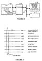
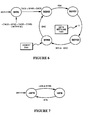
- a controller interface 100 which couples a microprocessor controller 102 to an IEEE 488 bus 104, which in turn is coupled to one or more devices 106, such as digital voltmeters, spectrum analyzers, oscilloscopes, or any other instrument which is designed to send and receive commands and messages via an IEEE 488 bus.
- the microprocessor 102 includes a DMA controller 108 which controls DMA data transfers and also outputs a "terminal count" signal TC for indicating the end of a particular data transfer sequence.
- the IEEE 488 bus 104 is also called the "GPIB" (general purpose interface bus ).
- the controller interface 100 in accordance with an embodiment of the present invention includes two "ports": a microprocessor port 120 and an IEEE 488 bus 104.
- the preferred embodiment of the invention will be described from the viewpoint of having a microprocessor controller coupled to port 120 and a variety of instruments 106 coupled to the IEEE 488 bus 104.
- this same circuit 100 can be used to couple the microprocessor inside an instrument 106 to the IEEE 488 bus 104.
- the interface 100 is a general purpose circuit for coupling either an instrument or a controller to the IEEE 488 bus 104.
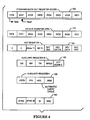
- the structure of the IEEE 488 bus 104 is shown in Figure 3. As shown, it has the following lines:
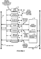
- Microprocessor port 120 contains a set of addressable data registers 122-130 for defining the interface's mode of operation, and for storing commands and messages being transmitted to and from the IEEE 488 bus 104.
- the data registers 122-130 in port 120 include an eight bit Command/Data Out Register (CDOR) 122 which is the general purpose register used for forwarding data, multiline messages, and commands from a controller to the IEEE 488 bus 104.
- CDOR Command/Data Out Register
- DIR Data In Register
- the Key Register 124 contains bit flags which specify the mode of communication with a microprocessor. Only the "200ns T1" bit is relevant to this embodiment of the present invention.
- the control circuitry for the CDOR 122 a local message, 'nba' (new byte available), which is true whenever a new byte of data is written into the CDOR.
- the Auxiliary Registers B and I 126 and 128 are used for functions not normally required by the IEEE 488 standard, some of which will be described below.
- Another register 130 stores SYNC and SYNC IE bits, described in more detail below.
- Other bits in this auxiliary register 130 include the END bit, and the DI (data in) bit.
- the END bit is set whenever the interface 100 accepts a message byte from a device on the GPIB 104 with the EOI line asserted, indicating that the last byte of a message has been sent.
- the DI bit is set whenever the interface 100 accepts a message byte from a device on the GPIB 104.
- the microprocessor port 120 also includes an instruction decoder 132 which decodes address, data and read/write signals from the microprocessor bus to generate local commands.
- the local command signals generated by the decoder 132 which are relevant to this embodiment of the present invention include: cont (continuous mode), rddir (read data in register), wrcdor (write to command/data out register) , rdhf (release handshake holdoff), hlda (holdoff on all), hlde (holdoff on end mode), hldi (holdoff immediate), holdoff (holdoff, i.e., stop transmission of further data), pon (power on reset), clear sync (clear SYNC bit to exit SYNC state), set sync (set SYNC bit), seoi (send EOI), and 'nbaf' (new byte available false) which resets the 'nba' (new byte available) signal generated by the CDOR 122.
- SYNC state machine 140 used for detecting when the IEEE 488 bus handshake is synchronized.
- the Source Handshake state machine 142 is used when "sourcing" messages or data to the bus 104. "Sourcing" means that data is being sent from the microprocessor to a device coupled to the GPIB 104.
- the Acceptor Handshake state machine 144 is used when accepting (i.e., receiving) multiline messages from a device on the GPIB 104.
- the Talker state machine 146 is used to control the transmission of device specific messages to devices on the GPIB 104.
- the Listener state machine 148 is used to control the reception of device specific messages from devices on the GPIB 104.
- the Service Request state machine 150 asserts the signal SRQ on the IEEE 488 bus to request services from the active bus controller.
- the Controller state machine 160 determines-when the Source Handshake State Machine 142 is used to send interface messages (e.g., trigger, clear, and addressing messages) to devices on the GPIB 104.
- the Controller state machine 160 also handles service requests by devices on the GPIB 104.
- the state machines shown in Figure 2 are interconnected by internal busses and signal lines 162 so that each state machine can use signals from the others.
- a data settling period of at least 350 nanoseconds is required before multiline messages or data sent by a controller are valid on the IEEE 488 bus. It should be noted that in some circumstances the T1 data settling period must be 500 nanoseconds or 2 microseconds, depending on the system configuration. Further, the first byte of each message requires additional settling time.
- T1 This data settling period
- data is valid on the microprocessor's data bus for at least 150 nanoseconds before the trailing edge of its write strobe signal. Therefore, the speed of data communications can be improved by overlapping the T1 data settling period with the last 150 nanoseconds of the write strobe, at least in those circumstances where it is known that the data on the controller's bus is valid during that 150 nanosecond period.
- the preferred embodiment of the present invention takes advantage of this overlap by setting the 200ns T1 bit, which, when set, instructs the Source Handshake circuit to count only 200 nanoseconds after the trailing edge of the write strobe instead of 350 nanoseconds.
- the Command/Data Out Register is an 8-bit write-only register used to move data from the computer to the GPIB 104 when the interface is the GPIB Talker or the Active Controller. Outgoing data is separately latched by this register and is not destroyed by a read from the DIR (data in register).
- the GPIB Source Handshake (SH) function is initiated (i.e., the local message 'nba' - new byte available - is true) and the byte is transferred to the GPIB.
- This register may also be written by a direct memory access (DMA) controller.
- DMA direct memory access
- the CDOR is a transparent latch, thus changes on the microprocessor's data bus during write cycles to the CDOR are reflected on the GPIB data bus.
- the Key Register is a write-only register.
- the bit pattern of the KEYR is shown in Figure 4.
- AUXRB Auxiliary Register B
- the TRI bit in AUXRB determines the interface circuit's Source Handshake Timing, T1.
- the T1 delay can be reduced further by setting the VSTD bit in AUXRI or by setting the 200ns T1 bit in KEY Register 124.
- Auxiliary Register I (AUXRI). Setting the VSTD bit in AUXRI sets the value of the T1 delay used by the source handshake function for data setup to 350 nsec for the second and subsequent data bytes sent after ATN unasserts. If this bit is cleared, the value of T1 is determined by the TRI bit in AUXRB.
- Source Handshake (SH).
- the Source Handshake state machine differs from the state diagram shown in the IEEE 488.1 Specification. States SWNS and SIWS are removed. These states recorded the false transition of the local message new byte available ('nba').
- the source handshake state diagram for the preferred embodiment is shown in Figure 6.
- Source Idle State In SIDS the Source Handshake function is disabled. The Source Handshake function powers on in SIDS and goes from SIDS to SGNS whenever the interface 100 is in a state (Taken Active State(TACS), Serial Port Active State(SPAS), or Controller Active State(CACS)) where it needs to source bytes onto the GPIB 104. The Source Handshake function returns to SIDS within t2 if none of these states is active (t2 is specified and defined in IEEE Std 488.1).
- SGNS Source Generate State
- the interface 100 is driving the CDOR onto the DIO lines of the GPIB 104, but is waiting for either a command byte, data byte, or serial port response to become available before issuing a new byte available ('nba') message.
- the Source Handshake function goes from SGNS to SDYS1 when the local message 'nba' becomes true.
- Source Delay State 1 (SDYS1): In SDYS the Source Handshake function is driving the new byte in the CDOR onto the DIO lines of the GPIB 104 for a time of at least T1.
- the SH function leaves SDYS1 and enters SDYS2 after a time of T1 has elapsed.
- Source Delay State 2 (SDYS2): In SDYS2 the DIO lines have already been driven with valid data for at least T1, and the SH function is waiting for all listeners to unassert NRFD (not ready for data) before asserting DAV (data valid). The SH function leaves SDYS2 and enters STRS as soon as no listeners are asserting NRFD.
- STRS Source Transfer State
- the source handshake function remains in SDYS1 driving the contents of the CDOR on the GPIB DIO lines for the amount of time specified by the T1 time delay.
- T1 is determined by the value of the TRI, VSTD and 200ns T1 bits and by HSTS (see Figure 7 and the following Table).
- HSTS is entered after the first data byte after ATN unasserts is sent. This enables a shorter bus settling time for all subsequent bytes until ATN becomes true.
- HSTS is always FALSE when the interface is the active controller (i.e., when ATN is asserted).
- this scheme is implemented by using a multiple output time counter 180 which outputs five potential T1 trigger signals.
- the counter 180 is enabled only when the Source Handshake state machine (see Figure 6) is in the SDYS1 state.
- a simple multiplexer 182 selects the proper signal one of these five signals, based on the values of the HSTS, TRI, VSTD and 200ns T1 signals, and outputs it as the T1 signal, which is used to transistion from SDYS1 to SDYS2 in the Source Handshake state machine.
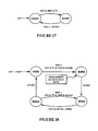
- a preferred embodiment of the present invention provides an enhancement to multibyte message processing by an IEEE 488 interface. More specifically, it provides a method of notifying the microprocessor, using an interrupt signal, that the last byte of an IEEE 488 message has been accepted by all listeners on the bus. To activate this enhanced function, the microprocessor writes a "1" into the SYNC IE (synchronization interrupt enable) bit of the register 130, shown in Figure 4. When the SYNC IE bit is set, and the SYNC state machine (shown in Figure 2) enters the SYNC state, an interrupt signal is sent to the microprocessor, notifying it that the end of the message has been reached.
- SYNC IE synchronization interrupt enable
- the SYNC function is not defined in IEEE Std 488. It controls a special SYNC bit in the interface circuit, which indicates that the GPIB has synchronized at the end of a transfer (the GPIB is said to be synchronized when DAV is unasserted after the last byte transferred). The SYNC bit is set at the completion of a transfer when the GPIB handshaking is complete.
- the SYNC function may actually be implemented as one state machine with very complex terms for its transitions, but since its usage is substantially different for DMA (direct memory access) reads, DMA writes, programmed I/O reads, and programmed I/O writes, four separate state diagrams are presented in the Figures. In all cases, the SYNC bit is set only in the SYNC state. Furthermore, an interrupt is generated (for prompting the microprocessor) only if the SYNC bit is set and the microprocessor has previously set the SYNC IE bit.
- DMA direct memory access
- the state diagram for the programmed I/O write version of the SYNC state machine is shown in Figure 8.
- the interface circuit must be in TACS (talker active state) or CACS (controller active state), and must not be using DMA for sourcing messages.
- Synchronized State In SYNC, the interface 100 is done with its current data transfer, the GPIB is synchronized, and the SYNC bit is set. The state machine exits SYNC and goes to WCWS if the SYNC bit is cleared (a 'clear sync' pulse is issued.) The microprocessor's driver software should issue a 'clear sync' command, which causes the interface to generate a 'clear sync' pulse that clears the SYNC bit before writing the last data byte of a programmed I/O transfer to the CDOR.
- WCWS Write Cycle Wait State
- Data Valid Wait State In DVWS the state machine is waiting for the byte to be sourced. The state machine exits DVWS and enters WSNS when DAV (data valid) is asserted (the last byte is being sourced).
- WSNS Wait for Synchronization State
- DMA Writes SYNC Function The state diagram for the SYNC state machine during DMA writes is shown in Figure 9. For the SYNC state machine to be in this mode the interface must be in TACS or CACS.
- Synchronized State In SYNC, the interface is done with its current data transfer, the GPIB is synchronized, and the SYNC bit is set. The SYNC state machine exits SYNC and goes to TCWS if a 'clear sync' command is issued. The driver software should clear the SYNC bit before beginning a DMA write operation.
- Terminal Count Wait State In the TCWS state, the SYNC state machine is waiting for a DMA write access to the CDOR with TC (terminal count) asserted (when the last byte of the DMA transfer is written to the CDOR). The SYNC state machine goes from TCWS to DVWS as soon as the DMA controller in the microprocessor writes the last byte of the message to the CDOR (as indicated by the TC signal).
- DVWS Data Valid Wait State
- WSNS Wait for Synchronization State
- the DMA controller For the SYNC function to be useful during DMA write operations the DMA controller must be capable of asserting the TC signal during the write cycle of the last byte to the CDOR.
- SYNC Sync State
- WSNS Wait for Synchronization State
- the SYNC bit will toggle with every byte during programmed I/O reads, therefore, the SYNC bit should not be polled or enabled for interrupts until after reading the last byte of a transfer from the DIR.
- the 'clear sync' command should not be issued during programmed I/O reads.
- DMA Reads SYNC Function The state diagram for the SYNC state machine during DMA reads is shown in Figure 11. For the SYNC state machine to be in this mode the interface must be in LACS.
- SYNC Sync State
- the interface 100 is done with its current data transfer, the GPIB is synchronized, and the SYNC bit is set.
- the SYNC state machine exits SYNC and goes to WCWS if the SYNC bit is cleared (the 'clear sync' command is issued).
- the driver software should clear the SYNC bit before beginning a DMA transfer.
- WCWS Write Cycle Wait State
- WSNS Wait for Synchronization State
- Synchronization State In SYNS the GPIB is synchronized (DAV is not asserted). The SYNC state machine exits SYNS and enters WSNS if DAV is asserted. If LBRS is active (which means that the last byte of the DMA transfer has been read by the DMA controller), the SYNC state machine exits SYNS and returns to SYNC.
- ⁇ LBRS Not Last Byte Read State
- Last Byte Read State In LBRS the last byte of the DMA transfer has been read from the DIR or the set sync command has been issued.
- the SYNC state machine exits LBRS and returns to ⁇ LBRS when the processor issues a 'clear SYNC' command.
- the SYNC function will toggle between WSNS and SYNS for each byte. While in SYNS the function will transfer to SYNC if LBRS is true. This will happen automatically if terminal count is reached while reading the last byte from the DIR (data input register). However, if this does not happen (i.e. a time-out or early END is detected) then LBRS can be set by issuing the 'set sync' command, which will cause the SYNC bit to set (i.e., the GPIB is synchronized).
- IEEE std 488 defines a local message, rfd (ready for data), which is issued before each byte of data is received by the microprocessor.
- the 'rfd' message is transmitted on the NRFD line of the bus (see Figure 3). Issuance of this local message affects GPIB signal lines in such a way as to permit the talker to send the next data byte over the GPIB.
- this local message is asserted automatically during a data transfer cycle whenever the interface is ready to receive another byte.
- the microprocessor After the last byte of a data transfer, however, it is necessary for the microprocessor to inhibit the local 'rfd' message, thereby preventing the talking device from sending further bytes. For example, if the application running in the microprocessor requested to read 100 bytes from a device, and for some reason the device had more than 100 bytes to send, transmission of the 101st byte must be inhibited until the application specifically requests more bytes. Since at the moment when the 100 bytes have been received it is unknown to the microprocessor whether the application needs or wants further bytes, or whether the application intends to cause subsequent bus activity, the safest course is to inhibit the arrival of further bytes.
- This embodiment of the present invention alleviates the need for this software intervention by allowing the last byte 'rfd' inhibition commands to be pre-programmed before the entire transfer begins. The entire transfer may then occur without the need to break it up, and the interface will correctly program itself before the last byte to inhibit the 'rfd' message. This feature, therefore, increases throughput and greatly decreases software complexity by eliminating the software intervention previously required by prior art devices.
- the direct memory access (DMA) controller in a microprocessor contains a counter that is used to determine when the last word or byte of a DMA transfer has been reached.
- the DMA controller outputs a signal, herein called TC, which is asserted when the DMA controller's counter reaches the value for the last word or byte to be read or written by the microprocessor.
- TC a signal used by the present invention to trigger a handshake holdoff when data is being accepted from the GPIB, and to trigger the generation of an END message when data is being sourced to the GPIB.
- the acceptor handshake function When the ACC bit is set during GPIB DMA reads, the acceptor handshake function will perform a RFD (ready for data) holdoff on the last byte read by the DMA controller (that is, the byte in which the TC signal is pulsed when read). Issuing the 'Finish Handshake' auxiliary command releases the holdoff.
- RFD ready for data
- Acceptor Handshake The Acceptor Handshake state diagram for the IEEE 488 interface 100 is shown in Figure 12. The following chart lists the outputs and actions of each of the acceptor handshake states.
- STATE RFD DAC Other Actions AIDS (T) (T) Acceptor Handshake is idle ANRS F F RFD Holdoff State ACRS (T) F Ready To Accept Data State ADYS F F If ATN is false - latch data into the DIR - set the DI (Data In) bit and END bit if appropriate If ATN is true - commands decoded and appropriate interrupts set - SDHS set if commands require DAC (data accepted) holdoff ACDS F F DAC Holdoff State AWNS F (T) Waiting for DAV to unassert (new cycle to begin)
- the implementation of the Acceptor Handshake in the present invention differs from the state diagram shown in the IEEE 488.1 Specification.
- the IEEE 488.1 state ACDS is divided into two states ADYS and ACDS.
- ADYS is entered after DAV is asserted and is the state in which data is strobed into the DIR and action is taken on the reception of GPIB commands. All interrupt status bits generated by the acceptor handshake are set by this state.
- the ACDS state is entered one clock cycle (Tah2) after ADYS is entered and is used as a holding state where the device will remain during DAC (data accepted) holdoffs.
- ANRS is the RFD holdoff state. To release the RFD holdoff either ATN must be asserted or the local message 'rdy' must be cleared.
- the Acceptor Handshake state machine uses five more state diagrams to implement the acceptor handshake function.
- the ADHS state diagram shown in Figure 13 is used to perform DAC holdoffs.
- ADHS is set if a command is received that the interface circuit 100 has been configured to perform a DAC holdoff (represented by SDHS in the state diagram).
- DAC holdoff can be released by issuing the 'valid' or 'nonvalid' commands which clears ADHS.
- Figure 13 shows the state diagram of the DAC Holdoff function.
- ANHS1&2, AEHS and CCHDF are implemented to perform RFD holdoffs.
- ANHS1 shown in Figure 14
- ADYS when ATN is false.
- ANHS1 indicates that a data byte was received and a RFD holdoff will occur to prevent the next data byte from being sent.
- the holdoff will be released when the data byte is read from the DIR unless one of several special holdoff conditions are enabled.
- the special holdoff conditions represented by holdoff in the state diagram
- the special holdoff conditions include holdoff on all (hlda) mode, continuous (cont) mode, holdoff on end (hlde) mode and AEHS set, ANHS2, or CCHDF.
- the ANHS2 state diagram shown in Figure 15 is used to holdoff the handshake immediately.
- ANHS2 is set by issuing the 'holdoff immediately' (hldi) auxiliary command and is cleared by issuing the 'release handshake holdoff' (rhdf) command.
- ANHS2 is not cleared by a 'pon' (power on reset), therefore it allows the control program to issue a 'holdoff immediately' (hldi) command while 'pon' is set and the interface circuit is being configured.
- the AEHS state diagram (shown in Figure 16) is implemented to record the reception of an END condition and allow a RFD holdoff to be performed afterward.
- AEHS is set on the reception of an END condition (i.e., when the last byte of the message is received) and is cleared when a 'release handshake holdoff' (rhdf) command is issued.
- the Carry Cycle Holdoff State Diagram (shown in Figure 17) is implemented to record the occurrence of a DMA Read of the DIR (rddir) with TC asserted and allows a RFD holdoff to be performed afterward if the automatic carry cycle bit (ACC) is set.
- CCHDF is cleared when the ACC bit is cleared or ANHS1 is false.
- the EOI Generation state diagram is shown in Figure 18.
- the EOI Generation state diagram is used to control the assertion of EOI by the interface while sourcing a data byte. If the 'Send EOI' auxiliary command (seoi) is issued followed by a write of the CDOR (wrcdor) while the interface is in TACS (talker active state), the EOI Generation state machine will enter ERAS and assert the GPIB EOI line. The function will enter ENAS as soon as the source handshake enters SDYS1 + SDYS2. EOI will remain asserted while in (ERAS or ENAS) and in (SDYS or STRS).
- auxiliary command 'nbaf' new byte available false
- the local message 'pon' always clear the EOI Generation function, forcing it into its idle state, ENIS.
Landscapes
- Engineering & Computer Science (AREA)
- Theoretical Computer Science (AREA)
- Physics & Mathematics (AREA)
- General Engineering & Computer Science (AREA)
- General Physics & Mathematics (AREA)
- Information Transfer Systems (AREA)
- Bus Control (AREA)
Claims (8)
- Interface de bus pour coupler un microprocesseur (102) à un bus (104) IEEE 488, ledit microprocesseur (102) ayant un contrôleur (108) d'accès direct à la mémoire qui génère un signal de compte terminal (TC) lors de la transmission de la dernière donnée dans un transfert de données multiples, ledit bus IEEE 488 (104) comportant des lignes de données et une ligne NON PRET POUR DONNEES (NRFD), l'interface comprenant :caractérisée par le fait queun accès (120) de microprocesseur pour transmettre et recevoir des données vers et en provenance dudit microprocesseur (102);des moyens (148) à circuit récepteur, couplés audit accès (120) du microprocesseur et audit bus (104) IEEE 488, pour transmettre des données dudit bus (104) IEEE 488 audit microprocesseur (102) par l'intermédiaire dudit accès (120) de microprocesseur ; etdes moyens (144) d'établissement de liaison accepteurs, couplés auxdits moyens (148) à circuit récepteur et audit bus (104) IEEE 488 ;ledit accès (120) de microprocesseur comporte des lignes de bus de données de microprocesseur et une ligne de compte terminal pour recevoir lesdits signaux TC dudit contrôleur (108) d'accès direct à la mémoire ; etlesdits moyens (144) d'établissement de liaison accepteurs comportent des moyens pour valider un signal de retenue sur ladite ligne NRFD dudit bus (104) IEEE 488 lorsque ledit accès (120) du microprocesseur reçoit un signal TC dudit contrôleur (108) d'accès direct à la mémoire tant qu'une condition prédéfinie n'est pas satisfaite ;de sorte que lesdits moyens (144) d'établissement de liaison accepteurs effectuent une retenue des données lors de la transmission de la dernière donnée pendant un transfert de données DMA à données multiples dudit bus (104) IEEE 488 audit microprocesseur (102).
- Interface selon la revendication 1, dans laquelle ledit bus (104) IEEE 488 comporte une ligne de donnée valide (DAV) ;ledit accès (120) de microprocesseur comporte au moins une ligne pour transmettre des signaux d'interruption à un accès de signal d'interruption dudit microprocesseur (102) ;lesdits moyens (144) d'établissement de liaison accepteurs comportent des moyens (130) pour détecter l'instant où le dernier octet d'un transfert de données a été reçu dudit bus (104) IEEE 488 pendant que lesdits moyens (148) à circuit récepteur transmettent des données audit microprocesseur (102) par l'intermédiaire dudit accès (120) de microprocesseur et pour transmettre ensuite un premier signal d'interruption audit accès de signal d'interruption dudit microprocesseur (102) par l'intermédiaire dudit accès (120) de microprocesseur ;ladite interface (100) comportant en outre :des moyens (140) de synchronisation, couplés audit bus (104) IEEE 488, pour détecter l'instant où un signal de donnée valide antérieurement validé sur ladite ligne DAV a été invalidé, et pour transmettre ensuite un second signal d'interruption audit accès de signal d'interruption dudit microprocesseur (102) par l'intermédiaire dudit accès (120) de microprocesseur ; etun commutateur (130) d'activation d'interruption de synchronisation pour activer lesdits moyens (140) de synchronisation afin d'envoyer ledit second signal d'interruption audit microprocesseur (102) ; lesdits moyens (140) de synchronisation n'envoyant pas ledit second signal d'interruption lorsqu'un signal de donnée valide préalablement validé sur ladite ligne DAV est invalidé sauf si ledit commutateur (130) d'autorisation d'interruption de synchronisation est activé ; ledit commutateur (130) d'activation d'interruption de synchronisation étant conçu pour être couplé audit processeur (102) par l'intermédiaire dudit accès (120) de microprocesseur afin que ledit microprocesseur (102) puisse activer et désactiver ledit commutateur (130) d'activation d'interruption de synchronisation ;de sorte que ledit microprocesseur (102) est automatiquement informé par ledit premier signal d'interruption du fait que le dernier octet d'un transfert de données a été transmis par ladite interface (100) dudit bus (104) IEEE 488 audit microprocesseur (102) et que ledit microprocesseur (102) est automatiquement informé par ledit second signal d'interruption du fait que ledit bus (104) IEEE 488 a achevé le transfert de données.
- Interface selon la revendication 2, comportant en outre :des moyens (146) à circuit émetteur, couplés audit accès (120) de microprocesseur et audit bus (104) IEEE 488 pour valider (injecter) des données reçues par ledit accès (120) de microprocesseur sur ledit bus (104) IEEE 488 ;des moyens (142) d'établissement de liaison avec la source, couplés auxdits moyens (146) à circuit émetteur et audit bus (104) IEEE 488, pour valider un signal de donnée valide sur ladite ligne DAV dudit bus (104) IEEE 488 après que lesdits moyens (146) à circuit émetteur ont validé les données sur ledit bus (104) IEEE 48 et pour invalider ledit signal de donnée valide en fonction d'un protocole d'établissement de liaison prédéfini avec la source ;lesdits moyens (140) de synchronisation étant conçus pour transmettre ledit second signal d'interruption audit accès de signal d'interruption dudit microprocesseur (102) par l'intermédiaire dudit accès (120) de microprocesseur lorsque lesdits moyens (142) d'établissement de liaison avec la source invalident ledit signal de donnée valide sur ladite ligne DAV et lorsque ledit commutateur (130) d'activation d'interruption de synchronisation est activé.
- Interface selon la revendication 3, dans laquelle ledit accès (120) de microprocesseur comporte une ligne d'écriture pour recevoir des impulsions d'écriture dudit processeur (102) ; chacune desdites impulsions d'écriture ayant une durée prédéfinie et un front descendant ; lesdits moyens (146) à circuit émetteur comportant un registre (122) à verrouillage transparent pour valider et verrouiller la donnée reçue dudit accès (120) de microprocesseur sur ledit bus (104) IEEE 488 de façon que la donnée reçue dudit accès (120) de microprocesseur soit validée sur ledit bus (104) IEEE 488 avant le front descendant desdites impulsions d'écriture ;lesdits moyens (142) d'établissement de liaison avec la source étant conçus pour valider un signal sur ladite ligne DAV dudit bus (104) IEEE 488 après que lesdits moyens (146) à circuit émetteur ont validé la donnée sur ledit bus (104) IEEE 488 pendant une première période de stabilisation minimale prédéfinie ;lesdits moyens (142) d'établissement de liaison avec la source comprenant des moyens (124, 126, 128, 180, 182) accélérateurs qui, lorsqu'ils sont activés, valident ledit signal sur ladite ligne DAV dudit bus (104) IEEE 488 après que lesdits moyens (146) à circuit émetteur ont validé la donnée sur ledit bus (104) IEEE 488 pendant une seconde période de stabilisation prédéfinie qui est inférieure à ladite première période de stabilisation minimale prédéfinie ; etladite interface (100) comportant un commutateur (124, 126, 128) d'activation de l'accélération pour activer lesdits moyens (124, 126, 128, 180, 182) d'accélération ;de sorte que la vitesse de transmission des données par ledit microprocesseur (102) est améliorée par réduction de ladite période de stabilisation.
- Interface selon la revendication 1, dans laquelle ledit bus (104) IEEE 488 comporte une ligne de donnée valide (DAV) ;ledit accès (120) de microprocesseur comporte au moins une ligne pour transmettre des signaux d'interruption à un accès de signal d'interruption dudit microprocesseur ;ladite interface (100) comportant en outre :des moyens (146) à circuit émetteur, couplés audit accès (120) de microprocesseur et audit bus (104) IEEE 488 pour valider (injecter) des données reçues par ledit accès (120) de microprocesseur sur ledit bus (104) IEEE 488 ;des moyens (140) de synchronisation couplés audit bus (104) IEEE 488, pour détecter l'instant où un signal de donnée valide précédemment validé sur ladite ligne DAV est invalidé, et pour transmettre ensuite un signal d'interruption de synchronisation audit accès de signal d'interruption dudit microprocesseur (102) par l'intermédiaire dudit accès (120) de microprocesseur ; etun commutateur (130) d'activation d'interruption de synchronisation pour activer lesdits moyens (140) de synchronisation afin d'envoyer ledit signal d'interruption de synchronisation audit microprocesseur (102) ; lesdits moyens (140) de synchronisation n'envoyant pas ledit signal d'interruption de synchronisation lorsqu'un signal de donnée valide précédemment validé sur ladite ligne DAV est invalidé, sauf si ledit commutateur (130) d'activation d'interruption de synchronisation est activé ;de sorte que ledit microprocesseur (102) est automatiquement informé par ledit signal d'interruption de synchronisation du fait que ledit bus (104) IEEE 488 a achevé le transfert de données.
- Interface selon la revendication 1, dans laquelle ledit bus (104) IEEE 488 comporte une ligne de donnée valide (DAV) ;ledit accès (120) de microprocesseur comporte une ligne d'écriture pour recevoir des impulsions d'écriture dudit microprocesseur (102) ; chacune desdites impulsions d'écriture ayant une durée et un front descendant prédéfinis ;des moyens (146) à circuit émetteur, couplés audit accès (120) de microprocesseur et audit bus (104) IEEE 488, pour valider les données reçues par ledit accès (120) de microprocesseur sur ledit bus (104) IEEE 488 ;lesdits moyens (146) à circuit émetteur comportant un registre (122) à verrouillage transparent pour valider et verrouiller une donnée reçue dudit accès (120) de microprocesseur sur ledit bus (104) IEEE 488, de façon que la donnée reçue dudit accès (120) de microprocesseur soit validée sur ledit bus (104) IEEE 488 avant le front descendant desdites impulsions d'écriture ; etdes moyens (142) d'établissement de liaison avec la source, couplés auxdits moyens (146) à circuit émetteur et audit bus (104) IEEE 488 pour valider un signal sur ladite ligne DAV dudit bus (104) IEEE 488 après que lesdits moyens (146) à circuit émetteur ont validé la donnée sur ledit bus (104) IEEE 488 pendant une première période de stabilisation minimale définie ;lesdits moyens (142) d'établissement de liaison avec la source comportant des moyens (124, 126, 128, 180, 182) d'accélération qui, lorsqu'ils sont activés, valident ledit signal sur ladite ligne DAV dudit bus (104) IEE 488 après que lesdits moyens (146) à circuit émetteur ont validé la donnée sur ledit bus (104) IEEE 488 pendant une seconde période de stabilisation prédéfinie qui est inférieure à ladite première période de stabilisation minimale prédéfinie ;de sorte que la vitesse de transmission des données par ledit microprocesseur (102) est améliorée par réduction de ladite période de stabilisation.
- Interface selon la revendication 6, comportant en outre un commutateur (124, 126, 128) d'activation de l'accélération pour activer lesdits moyens (124, 126, 128, 180, 182) d'accélération.
- Interface selon la revendication 6, dans laquelleledit accès (120) de microprocesseur comporte au moins une ligne pour transmettre des signaux d'interruption à un accès de signal d'interruption dudit microprocesseur (102) ;lesdits moyens (144) d'établissement de liaison accepteurs comportent des moyens pour détecter l'instant où le dernier octet d'un transfert de données a été reçu dudit bus (104) IEEE 488 tandis que lesdits moyens (148) à circuit récepteur transmettent des données audit microprocesseur (102) par l'intermédiaire dudit accès (120) de microprocesseur, et pour transmettre ensuite un premier signal d'interruption audit accès de signal d'interruption dudit microprocesseur (102) par l'intermédiaire dudit accès (120) de microprocesseur ; etdes moyens (140) de synchronisation, couplés audit bus (104) IEEE 488, pour détecter l'instant où un signal de donnée valide précédemment validé sur ladite ligne DAV a été invalidé, comportant des moyens pour transmettre ensuite un second signal d'interruption audit accès de signal d'interruption dudit microprocesseur (102) par l'intermédiaire dudit accès (120) de microprocesseur ; etun commutateur (130) d'activation d'interruption de synchronisation pour activer lesdits moyens (140) de synchronisation afin d'envoyer ledit signal d'interruption audit microprocesseur (102) ; lesdits moyens (140) de synchronisation n'envoyant pas ledit second signal d'interruption lorsqu'un signal de donnée valide précédemment validé sur ladite ligne DAV est invalidé, sauf si ledit commutateur (130) d'activation d'interruption de synchronisation est activé ;de sorte que ledit microprocesseur (102) est automatiquement informé par ledit premier signal d'interruption du fait que le dernier octet d'un transfert de données a été transmis par ladite interface (100) dudit bus (104) IEEE 488 audit microprocesseur (102) et que ledit microprocesseur est automatiquement informé par ledit second signal d'interruption du fait que tous les autres dispositifs (106) sur ledit bus (104) IEEE 488 ont accepté le dernier octet d'un transfert de données.
Priority Applications (1)
| Application Number | Priority Date | Filing Date | Title |
|---|---|---|---|
| EP97110553A EP0805400B1 (fr) | 1990-07-03 | 1991-07-02 | Interface IEEE488 et méthode de traitement de message |
Applications Claiming Priority (2)
| Application Number | Priority Date | Filing Date | Title |
|---|---|---|---|
| US07/548,293 US5287528A (en) | 1990-07-03 | 1990-07-03 | IEEE 488 interface for message handling method |
| US548293 | 1995-11-01 |
Related Child Applications (1)
| Application Number | Title | Priority Date | Filing Date |
|---|---|---|---|
| EP97110553A Division EP0805400B1 (fr) | 1990-07-03 | 1991-07-02 | Interface IEEE488 et méthode de traitement de message |
Publications (3)
| Publication Number | Publication Date |
|---|---|
| EP0465221A2 EP0465221A2 (fr) | 1992-01-08 |
| EP0465221A3 EP0465221A3 (en) | 1993-02-24 |
| EP0465221B1 true EP0465221B1 (fr) | 1998-03-04 |
Family
ID=24188208
Family Applications (2)
| Application Number | Title | Priority Date | Filing Date |
|---|---|---|---|
| EP91305995A Expired - Lifetime EP0465221B1 (fr) | 1990-07-03 | 1991-07-02 | Interface IEEE488 |
| EP97110553A Expired - Lifetime EP0805400B1 (fr) | 1990-07-03 | 1991-07-02 | Interface IEEE488 et méthode de traitement de message |
Family Applications After (1)
| Application Number | Title | Priority Date | Filing Date |
|---|---|---|---|
| EP97110553A Expired - Lifetime EP0805400B1 (fr) | 1990-07-03 | 1991-07-02 | Interface IEEE488 et méthode de traitement de message |
Country Status (4)
| Country | Link |
|---|---|
| US (2) | US5287528A (fr) |
| EP (2) | EP0465221B1 (fr) |
| JP (1) | JP3377798B2 (fr) |
| DE (2) | DE69128985T2 (fr) |
Families Citing this family (17)
| Publication number | Priority date | Publication date | Assignee | Title |
|---|---|---|---|---|
| AU5990194A (en) * | 1993-05-10 | 1994-12-12 | Taligent, Inc. | Audio synchronization system |
| JP3608804B2 (ja) * | 1993-05-14 | 2005-01-12 | 株式会社ソニー・コンピュータエンタテインメント | バス制御装置 |
| US5572525A (en) * | 1995-05-31 | 1996-11-05 | National Instruments Corporation | GPIB extender with find listener protocol capabilities |
| US5649123A (en) * | 1995-06-07 | 1997-07-15 | National Instruments Corporation | GPIB system with improved parallel poll response detection |
| US5649129A (en) * | 1995-06-07 | 1997-07-15 | National Instruments Corporation | GPIB system including controller and analyzer |
| US6256660B1 (en) * | 1997-04-08 | 2001-07-03 | International Business Machines Corporation | Method and program product for allowing application programs to avoid unnecessary packet arrival interrupts |
| US6167480A (en) * | 1997-06-25 | 2000-12-26 | Advanced Micro Devices, Inc. | Information packet reception indicator for reducing the utilization of a host system processor unit |
| US10820949B2 (en) | 1999-04-07 | 2020-11-03 | Intuitive Surgical Operations, Inc. | Medical robotic system with dynamically adjustable slave manipulator characteristics |
| US6594552B1 (en) * | 1999-04-07 | 2003-07-15 | Intuitive Surgical, Inc. | Grip strength with tactile feedback for robotic surgery |
| US6831926B1 (en) | 2000-10-27 | 2004-12-14 | The Boeing Company | Legacy signals databus adapter/coupler |
| US6567966B2 (en) * | 2001-02-14 | 2003-05-20 | Agilent Technologies, Inc. | Interweaved integrated circuit interconnects |
| US7594026B1 (en) * | 2001-04-25 | 2009-09-22 | Zarlink Semiconductor (U.S.) Inc. | Method and apparatus for multi-phy communication without an ATM bus master |
| US6898723B2 (en) * | 2002-04-01 | 2005-05-24 | Mitac International Corp. | Method for verifying clock signal frequency of computer sound interface that involves checking whether count value of counter is within tolerable count range |
| US7005846B2 (en) * | 2002-07-17 | 2006-02-28 | Agilent Technologies, Inc. | System and method for application control in measurement devices |
| EP2341445B1 (fr) | 2009-12-30 | 2017-09-06 | Intel Deutschland GmbH | Procédé pour le transfert de données à haute vitesse |
| EP2434404B1 (fr) | 2010-09-27 | 2017-08-23 | Intel Deutschland GmbH | Procédé et arrangement pour le profilage de données de diffusion en continu |
| US11030903B2 (en) * | 2018-05-30 | 2021-06-08 | Ford Global Technologies, Llc | Vehicle-to-infrastructure communication |
Family Cites Families (8)
| Publication number | Priority date | Publication date | Assignee | Title |
|---|---|---|---|---|
| US4319338A (en) * | 1979-12-12 | 1982-03-09 | Allen-Bradley Company | Industrial communications network with mastership determined by need |
| US4402055A (en) * | 1981-01-27 | 1983-08-30 | Westinghouse Electric Corp. | Automatic test system utilizing interchangeable test devices |
| US4396995A (en) * | 1981-02-25 | 1983-08-02 | Ncr Corporation | Adapter for interfacing between two buses |
| US4534011A (en) * | 1982-02-02 | 1985-08-06 | International Business Machines Corporation | Peripheral attachment interface for I/O controller having cycle steal and off-line modes |
| US4523310A (en) * | 1983-01-28 | 1985-06-11 | Gould Computer Systems Inc. | Synchronous communications multiplexer |
| US4680788A (en) * | 1983-08-31 | 1987-07-14 | Data General Corporation | Microprocessor based control and switching device |
| US4727370A (en) * | 1985-12-17 | 1988-02-23 | Ampex Corporation | Method and system for synchronous handshake generation |
| US4982325A (en) * | 1988-03-18 | 1991-01-01 | At&T Bell Laboratories | Applications processor module for interfacing to a database system |
-
1990
- 1990-07-03 US US07/548,293 patent/US5287528A/en not_active Expired - Lifetime
-
1991
- 1991-07-02 EP EP91305995A patent/EP0465221B1/fr not_active Expired - Lifetime
- 1991-07-02 DE DE69128985T patent/DE69128985T2/de not_active Expired - Lifetime
- 1991-07-02 DE DE69132786T patent/DE69132786T2/de not_active Expired - Lifetime
- 1991-07-02 EP EP97110553A patent/EP0805400B1/fr not_active Expired - Lifetime
- 1991-07-03 JP JP16259991A patent/JP3377798B2/ja not_active Expired - Lifetime
-
1993
- 1993-11-18 US US08/154,867 patent/US5572684A/en not_active Expired - Lifetime
Also Published As
| Publication number | Publication date |
|---|---|
| DE69132786T2 (de) | 2002-05-08 |
| US5572684A (en) | 1996-11-05 |
| EP0805400B1 (fr) | 2001-10-24 |
| EP0805400A1 (fr) | 1997-11-05 |
| JPH05181790A (ja) | 1993-07-23 |
| DE69128985T2 (de) | 1998-09-10 |
| JP3377798B2 (ja) | 2003-02-17 |
| US5287528A (en) | 1994-02-15 |
| DE69132786D1 (de) | 2001-11-29 |
| EP0465221A2 (fr) | 1992-01-08 |
| EP0465221A3 (en) | 1993-02-24 |
| DE69128985D1 (de) | 1998-04-09 |
Similar Documents
| Publication | Publication Date | Title |
|---|---|---|
| EP0465221B1 (fr) | Interface IEEE488 | |
| EP0009678B1 (fr) | Dispositif d'entrée/sortie pour ordinateur | |
| US6173349B1 (en) | Shared bus system with transaction and destination ID | |
| JP3604398B2 (ja) | 並列パケット化されたモジュール期調停高速制御およびデータバス | |
| US4631670A (en) | Interrupt level sharing | |
| US5812875A (en) | Apparatus using a state device and a latching circuit to generate an acknowledgement signal in close proximity to the request signal for enhancing input/output controller operations | |
| US5159684A (en) | Data communication interface integrated circuit with data-echoing and non-echoing communication modes | |
| JPH02227765A (ja) | デジタル・コンピユータのデータ転送装置 | |
| US5475846A (en) | Apparatus for processing PCMCIA interrupt requests | |
| EP0030978B1 (fr) | Systeme de commande de transfert d'informations | |
| US4120029A (en) | Method and apparatus for recovering a signal transferred over a common bus in a data processing system | |
| US5315706A (en) | High speed IEEE 488 bus interface system and method | |
| US5608883A (en) | Adapter for interconnecting single-ended and differential SCSI buses to prevent `busy` or `wired-or` glitches from being passed from one bus to the other | |
| JPS58502027A (ja) | 低デ−タ転送率の直列入出力インタ−フェイスをモニタするようにされた周辺装置 | |
| US5694586A (en) | Controller using time-domain filter connected to a signal line to control a time at which signal line is sampled for receipt of information transfer signal | |
| US5964853A (en) | Interface controller including hardware mechanism to handle PS/2 interface | |
| US5640570A (en) | Information handling system for transmitting contents of line register from asynchronous controller to shadow register in another asynchronous controller determined by shadow register address buffer | |
| EP0577110A2 (fr) | Système d'interface à double bus pour réseaux locaux | |
| US6052746A (en) | Integrated circuit having programmable pull device configured to enable/disable first function in favor of second function according to predetermined scheme before/after reset | |
| US6408353B1 (en) | Microcomputer having sampling function of retry requesting signal in syncronization with strobe signal | |
| US5428797A (en) | Circuitry for eliminating bus contention at high frequencies by driving a bus to an available state prior to its relinquishing control of the bus | |
| RU2018944C1 (ru) | Устройство для сопряжения эвм с внешними объектами | |
| JPH07244633A (ja) | インタフェース装置 | |
| KR900000610B1 (ko) | 컴퓨터용 라인프린터의 인터페이스 제어장치 | |
| JPH05101016A (ja) | キヤツシユスヌーピング制御装置 |
Legal Events
| Date | Code | Title | Description |
|---|---|---|---|
| PUAI | Public reference made under article 153(3) epc to a published international application that has entered the european phase |
Free format text: ORIGINAL CODE: 0009012 |
|
| AK | Designated contracting states |
Kind code of ref document: A2 Designated state(s): BE CH DE FR GB IT LI NL |
|
| RIN1 | Information on inventor provided before grant (corrected) |
Inventor name: ODOM, BRIAN K. Inventor name: NOWLIN, WILLIAM C., JR. Inventor name: CANIK, ROBERT |
|
| PUAL | Search report despatched |
Free format text: ORIGINAL CODE: 0009013 |
|
| AK | Designated contracting states |
Kind code of ref document: A3 Designated state(s): BE CH DE FR GB IT LI NL |
|
| 17P | Request for examination filed |
Effective date: 19930309 |
|
| 17Q | First examination report despatched |
Effective date: 19951204 |
|
| GRAG | Despatch of communication of intention to grant |
Free format text: ORIGINAL CODE: EPIDOS AGRA |
|
| GRAG | Despatch of communication of intention to grant |
Free format text: ORIGINAL CODE: EPIDOS AGRA |
|
| GRAH | Despatch of communication of intention to grant a patent |
Free format text: ORIGINAL CODE: EPIDOS IGRA |
|
| GRAH | Despatch of communication of intention to grant a patent |
Free format text: ORIGINAL CODE: EPIDOS IGRA |
|
| GRAH | Despatch of communication of intention to grant a patent |
Free format text: ORIGINAL CODE: EPIDOS IGRA |
|
| GRAA | (expected) grant |
Free format text: ORIGINAL CODE: 0009210 |
|
| AK | Designated contracting states |
Kind code of ref document: B1 Designated state(s): BE CH DE FR GB IT LI NL |
|
| PG25 | Lapsed in a contracting state [announced via postgrant information from national office to epo] |
Ref country code: IT Free format text: LAPSE BECAUSE OF FAILURE TO SUBMIT A TRANSLATION OF THE DESCRIPTION OR TO PAY THE FEE WITHIN THE PRE;WARNING: LAPSES OF ITALIAN PATENTS WITH EFFECTIVE DATE BEFORE 2007 MAY HAVE OCCURRED AT ANY TIME BEFORE 2007. THE CORRECT EFFECTIVE DATE MAY BE DIFFERENT FROM THE ONE RECORDED.SCRIBED TIME-LIMIT Effective date: 19980304 Ref country code: BE Free format text: LAPSE BECAUSE OF FAILURE TO SUBMIT A TRANSLATION OF THE DESCRIPTION OR TO PAY THE FEE WITHIN THE PRESCRIBED TIME-LIMIT Effective date: 19980304 Ref country code: NL Free format text: LAPSE BECAUSE OF FAILURE TO SUBMIT A TRANSLATION OF THE DESCRIPTION OR TO PAY THE FEE WITHIN THE PRESCRIBED TIME-LIMIT Effective date: 19980304 Ref country code: CH Free format text: LAPSE BECAUSE OF FAILURE TO SUBMIT A TRANSLATION OF THE DESCRIPTION OR TO PAY THE FEE WITHIN THE PRESCRIBED TIME-LIMIT Effective date: 19980304 Ref country code: LI Free format text: LAPSE BECAUSE OF FAILURE TO SUBMIT A TRANSLATION OF THE DESCRIPTION OR TO PAY THE FEE WITHIN THE PRESCRIBED TIME-LIMIT Effective date: 19980304 |
|
| XX | Miscellaneous (additional remarks) |
Free format text: TEILANMELDUNG 97110553.1 EINGEREICHT AM 27/06/97. |
|
| REG | Reference to a national code |
Ref country code: CH Ref legal event code: EP |
|
| REF | Corresponds to: |
Ref document number: 69128985 Country of ref document: DE Date of ref document: 19980409 |
|
| ET | Fr: translation filed | ||
| NLV1 | Nl: lapsed or annulled due to failure to fulfill the requirements of art. 29p and 29m of the patents act | ||
| REG | Reference to a national code |
Ref country code: CH Ref legal event code: PL |
|
| PLBE | No opposition filed within time limit |
Free format text: ORIGINAL CODE: 0009261 |
|
| STAA | Information on the status of an ep patent application or granted ep patent |
Free format text: STATUS: NO OPPOSITION FILED WITHIN TIME LIMIT |
|
| 26N | No opposition filed | ||
| REG | Reference to a national code |
Ref country code: GB Ref legal event code: IF02 |
|
| PGFP | Annual fee paid to national office [announced via postgrant information from national office to epo] |
Ref country code: FR Payment date: 20100805 Year of fee payment: 20 Ref country code: DE Payment date: 20100630 Year of fee payment: 20 Ref country code: GB Payment date: 20100630 Year of fee payment: 20 |
|
| REG | Reference to a national code |
Ref country code: DE Ref legal event code: R071 Ref document number: 69128985 Country of ref document: DE |
|
| REG | Reference to a national code |
Ref country code: DE Ref legal event code: R071 Ref document number: 69128985 Country of ref document: DE |
|
| REG | Reference to a national code |
Ref country code: GB Ref legal event code: PE20 Expiry date: 20110701 |
|
| PG25 | Lapsed in a contracting state [announced via postgrant information from national office to epo] |
Ref country code: GB Free format text: LAPSE BECAUSE OF EXPIRATION OF PROTECTION Effective date: 20110701 |
|
| PG25 | Lapsed in a contracting state [announced via postgrant information from national office to epo] |
Ref country code: DE Free format text: LAPSE BECAUSE OF EXPIRATION OF PROTECTION Effective date: 20110703 |