EP0465806A2 - Détecteur de distances à intégration de charges - Google Patents
Détecteur de distances à intégration de charges Download PDFInfo
- Publication number
- EP0465806A2 EP0465806A2 EP91108460A EP91108460A EP0465806A2 EP 0465806 A2 EP0465806 A2 EP 0465806A2 EP 91108460 A EP91108460 A EP 91108460A EP 91108460 A EP91108460 A EP 91108460A EP 0465806 A2 EP0465806 A2 EP 0465806A2
- Authority
- EP
- European Patent Office
- Prior art keywords
- radiation
- pulse
- array
- distance
- pulses
- Prior art date
- Legal status (The legal status is an assumption and is not a legal conclusion. Google has not performed a legal analysis and makes no representation as to the accuracy of the status listed.)
- Withdrawn
Links
- 230000010354 integration Effects 0.000 title description 16
- 230000005855 radiation Effects 0.000 claims abstract description 116
- 238000000034 method Methods 0.000 claims abstract description 22
- 230000001419 dependent effect Effects 0.000 claims abstract description 18
- 230000000977 initiatory effect Effects 0.000 claims 1
- 238000001514 detection method Methods 0.000 abstract description 37
- 239000000835 fiber Substances 0.000 description 25
- 230000003287 optical effect Effects 0.000 description 24
- 239000013307 optical fiber Substances 0.000 description 15
- 230000008901 benefit Effects 0.000 description 9
- 230000035945 sensitivity Effects 0.000 description 9
- 238000003384 imaging method Methods 0.000 description 8
- 238000005259 measurement Methods 0.000 description 8
- 238000003491 array Methods 0.000 description 7
- 230000008569 process Effects 0.000 description 7
- 238000010586 diagram Methods 0.000 description 6
- 230000004044 response Effects 0.000 description 6
- 238000012546 transfer Methods 0.000 description 6
- 229910001218 Gallium arsenide Inorganic materials 0.000 description 5
- 230000003466 anti-cipated effect Effects 0.000 description 4
- 230000003111 delayed effect Effects 0.000 description 4
- 238000005516 engineering process Methods 0.000 description 4
- 230000003595 spectral effect Effects 0.000 description 4
- 230000005540 biological transmission Effects 0.000 description 3
- 238000012545 processing Methods 0.000 description 3
- 229910000661 Mercury cadmium telluride Inorganic materials 0.000 description 2
- 238000013459 approach Methods 0.000 description 2
- 238000004364 calculation method Methods 0.000 description 2
- 238000004519 manufacturing process Methods 0.000 description 2
- 239000004065 semiconductor Substances 0.000 description 2
- 238000009825 accumulation Methods 0.000 description 1
- 230000002411 adverse Effects 0.000 description 1
- 238000001444 catalytic combustion detection Methods 0.000 description 1
- 230000008859 change Effects 0.000 description 1
- 230000001427 coherent effect Effects 0.000 description 1
- 239000002131 composite material Substances 0.000 description 1
- 230000007812 deficiency Effects 0.000 description 1
- 230000001934 delay Effects 0.000 description 1
- 238000013461 design Methods 0.000 description 1
- 230000008030 elimination Effects 0.000 description 1
- 238000003379 elimination reaction Methods 0.000 description 1
- 230000006870 function Effects 0.000 description 1
- WPYVAWXEWQSOGY-UHFFFAOYSA-N indium antimonide Chemical compound [Sb]#[In] WPYVAWXEWQSOGY-UHFFFAOYSA-N 0.000 description 1
- -1 lead-salt Chemical compound 0.000 description 1
- 238000012423 maintenance Methods 0.000 description 1
- 238000013507 mapping Methods 0.000 description 1
- 238000012986 modification Methods 0.000 description 1
- 230000004048 modification Effects 0.000 description 1
- 238000012544 monitoring process Methods 0.000 description 1
- 230000010363 phase shift Effects 0.000 description 1
- 238000010248 power generation Methods 0.000 description 1
- 230000009467 reduction Effects 0.000 description 1
- 238000011160 research Methods 0.000 description 1
- 230000002441 reversible effect Effects 0.000 description 1
- 239000010979 ruby Substances 0.000 description 1
- 229910001750 ruby Inorganic materials 0.000 description 1
- 238000000926 separation method Methods 0.000 description 1
- 239000000779 smoke Substances 0.000 description 1
- 239000007787 solid Substances 0.000 description 1
- 230000001360 synchronised effect Effects 0.000 description 1
Images







Classifications
-
- G—PHYSICS
- G01—MEASURING; TESTING
- G01S—RADIO DIRECTION-FINDING; RADIO NAVIGATION; DETERMINING DISTANCE OR VELOCITY BY USE OF RADIO WAVES; LOCATING OR PRESENCE-DETECTING BY USE OF THE REFLECTION OR RERADIATION OF RADIO WAVES; ANALOGOUS ARRANGEMENTS USING OTHER WAVES
- G01S17/00—Systems using the reflection or reradiation of electromagnetic waves other than radio waves, e.g. lidar systems
- G01S17/88—Lidar systems specially adapted for specific applications
- G01S17/89—Lidar systems specially adapted for specific applications for mapping or imaging
-
- G—PHYSICS
- G01—MEASURING; TESTING
- G01S—RADIO DIRECTION-FINDING; RADIO NAVIGATION; DETERMINING DISTANCE OR VELOCITY BY USE OF RADIO WAVES; LOCATING OR PRESENCE-DETECTING BY USE OF THE REFLECTION OR RERADIATION OF RADIO WAVES; ANALOGOUS ARRANGEMENTS USING OTHER WAVES
- G01S17/00—Systems using the reflection or reradiation of electromagnetic waves other than radio waves, e.g. lidar systems
- G01S17/02—Systems using the reflection of electromagnetic waves other than radio waves
- G01S17/50—Systems of measurement based on relative movement of target
Definitions
- the present invention relates to the use of radiation to measure the distance and velocity of an object of interest. More particularly, the present invention relates to a charge integration ranger which utilizes radiation pulses, knowledge of the velocity of light and a charge transfer device detector to measure the distance and velocity of an object and provide three-dimensional imaging.
- Telemetry systems which determine object distance using optical radiation are known. Such systems send radiation towards a distant object and measure distance based on the reflected radiation that returns to the system. Distance is determined based on one of several types of calculations, including triangulation, frequency changes in the returned radiation, and the time the optical radiation takes to reach the object and return to the system.
- heterodyne detection One technique for measuring distance and velocity that has received widespread attention in recent years is heterodyne or coherent detection.
- the frequency of an emitted optical radiation signal is modulated so that optical heterodyne detection can be employed.
- optical heterodyne detection implies that some sort of interferometer is employed in the receiver for aiding in phase comparison.
- the main advantages of heterodyne detection include narrowband signals, a high signal-to-noise ratio (SNR), shot-noise-limited performance and the ability to measure Doppler frequency shift in order to determine radial velocity.
- SNR signal-to-noise ratio
- shot-noise-limited performance the ability to measure Doppler frequency shift in order to determine radial velocity.
- optical heterodyne detection requires a relatively low energy optical radiation source, permits detection at the quantum noise limit, and is theoretically more sensitive than known direct detection techniques.
- heterodyne detection poses a number of difficulties that may, even under mildly adverse conditions, severely affect performance. For example, large object velocities require high detector bandwidths. High bandwidth detectors normally have a higher noise equivalent power and other undesirable characteristics. Additionally, without some prior knowledge of the signal location, narrow bandwidth signals at high frequencies require long search times or a large number of tuned filters. Further, interferometers are extremely sensitive devices which require precise phase front control. Any sort of unwanted phase perturbation, whether produced by or in the interferometer or by the laser source feeding the interferometer, will degrade the signal and can be considered noise. Many other sources of noise also exist.
- noises such as detector, background, electronic and local oscillator shot noises
- noise sources include modulation instability and distortion, optical misalignment and imperfections, vibrations, atmospheric turbulence, object vibration and rotation, and reflection modulation.
- heterodyne detection theoretically offers a great number of advantages, it is not presently practical for many applications. Extensive engineering is required to minimize the noise sources, and these required noise reduction techniques are complex, difficult to implement and expensive. Further, such techniques may require continuous monitoring, which further reduces the applicability of heterodyne detection.
- Direct detection is widely used in range finding systems.
- Simple implementations of direct detection systems employ an array of light-sensitive diodes which has a known mathematical relationship with a radiation source so that the distance of an object can be determined by trigonometric methods, such as triangulation.
- these systems are used in cameras for determining the range of an object to be photographed for focusing an automatic lens.
- such systems have limited applications because of limited range capability and relatively poor range resolution.
- U.S. Patent No. 4,522,492 to Masunaga discloses a distance measuring device which includes an infrared emitting portion having an infrared emitting diode and a projection lens, and an infrared receiving portion which includes a receiving lens and a line sensor comprising light-sensitive elements. Since this system measures distance by triangulation, the object to be measured must be positioned along the optical axis of the infrared emitting portion. Additionally, a line from the emitting lens to the receiving lens is perpendicular to the optical axis, and the two lenses must be a known distance apart.
- Distance to the object is calculated based upon which light-sensitive element in the line sensor receives the infrared light reflected from the object, as the two non-right angles in a right triangle created with the object can be determined, since the distance between the light-sensitive element and the optical axis is known.
- applications of such a system are limited to situations where the exact direction of an object to be ranged is known, since the object must be aligned along the optical axis of the infrared emitting portion. Further, only distance can be measured.
- a second direct detection system is disclosed in U.S. Patent No. 4,746,790 to Sorimachi.
- a pair of light receiving portions are utilized each comprising a lens and an array of light-sensitive elements.
- the arrays can be comprised of charge-coupled device (CCD) arrays.
- CCD charge-coupled device
- the object to be ranged is aligned along the optical axis of a first portion, and the lens of the second portion, the CCD array, or both are moved until light reflected from the object is received by a predetermined element of the CCD array of the second portion.
- the distance between the lenses is known, and any movement of the lens and/or the array is measured so that the distance of the object can be determined by triangulation.
- This system has the same limitations as the Masunaga system.
- an object of the present invention is to provide a direct detection system which provides the performance advantages of a heterodyne range detection system but is more reliable, less complex and less expensive to manufacture than a heterodyne detection systems.
- a further object of the present invention is to provide a direct detection system which requires a relatively low optical power.
- Another object of the present invention is to provide a ranging system having an extremely fast update time.
- Yet another object of the present invention is to provide a direct detection system which is not limited to detecting the distance of an object on its optical axis.
- Still another object of the present invention is to provide a direct detection system which is capable of three-dimensional imaging.
- a still further object of the present invention is to provide an optical ranging system capable of using any of a variety of lasers, including semiconductor, solid state and gas lasers at differing wavelengths and power levels.
- One still further object of the present invention is to provide an optical detection system which will not damage the vision of its users.
- An additional object of the present invention is to provide an optical ranging system of reduced complexity which can perform both ranging and velocity detection.
- a ranging system comprises: a transmitter for transmitting a series of at least one radiation pulse to an object area based on a command signal; a receiver for receiving returning radiation reflected off an object in the object area and selectively redirecting the returning radiation from each pulse dependent upon the command signal and object characteristics; and at least two radiation detectors arranged to receive the redirected returning radiation from the receiver, each of the radiation detectors being representative of different object data.
- Object data is determined based on which of the radiation detectors receives the redirected returning radiation.
- the radiation pulses are laser pulses and the transmitter includes a laser and a laser controller for transmitting laser pulses based upon the command signal.
- the receiver may include a scanning mirror and a scanning mirror controller for causing the mirror to scan relative to each laser pulse based upon the command signal so that the returning radiation from each pulse is redirected to strike one of the radiation detectors dependent upon the distance of the object.
- the radiation detectors comprise pixels in a one-dimensional CCD array
- the object characteristics include a distance range defined by a minimum and a maximum distance in which an object is to be sought, the distance range being scanned by delaying the start of the scanning of the mirror and controlling the speed of the scanning of the mirror relative to each pulse based upon the speed of light and the time necessary for a pulse to reach and return from the minimum distance and the maximum distance in the distance range.
- the radiation detectors comprise pixels, returning radiation from each pulse is stored as a charge in one or more of the pixels, and after integration of the series of pixels the charges are read out of the CCD array.
- the present invention also discloses a method for obtaining object data.
- the method provides the steps of transmitting a radiation pulse to an object area; scanning relative to the radiation pulse returning radiation received from the object area across a radiation-sensitive array so that returning radiation from the radiation pulse reflected from an object in the object area strikes a position on the radiation sensitive array dependent upon distance to the object and determining the distance to the object based on the position on the radiation-sensitive array which received the reflected radiation.
- the scanning can be delayed relative to the transmission of the radiation pulse so that a desired distance range only is scanned for an object.
- a system for determining characteristics of an object comprising a generator and transmitter for generating and transmitting a series of pulses toward an object area dependent upon a control signal, a focusing system for focusing the returning radiation from the radiation pulses, and a receiver for receiving and storing the returning radiation from the object area, the receiver being positioned proximate to a focal point of the focusing system.
- the receiver is continuously scanned based on the control signal so that the returning radiation is accumulated at locations within the receiver based on distance to the object.
- the receiver can comprise a one-dimensional CCD array having a predetermined number of pixels, with the focusing system focusing returning radiation onto one of the pixels.
- the CCD array shifts charges from pixel to pixel during the anticipated radiation return time period.
- Each pixel is representative of a distance to the object, but distance to an object can be determined to sub-pixel resolution by determining the multiple-pulse centroid on the CCD array.
- the present invention also discloses a three-dimensional imaging system comprising a transmitter for transmitting a radiation pulse to an object in an object area; a receiver including a focusing system for focusing the returning radiation and a plurality of optical fibers having a first end arranged in a common focal plane of the focusing system for receiving returning radiation relative to respective points in the object area; and a CCD array having a set of pixels dedicated for each optical fiber, each set being located proximate to a second end of one of the optical fibers for receiving and storing as a charge radiation received at the first end of each optical fiber.
- the charge integration range detector of the present invention is a direct detection device which has overcome the low sensitivity and poor noise characteristic problems of the prior art direct detection devices. This is accomplished by using the natural charge integration characteristics of charge transfer device (CTD) detectors such as charge coupled devices (CCD).
- CCD charge transfer device
- the charge integration range detector of the present invention operates by mapping time of flight data of radiation pulses into position(s) along a linear array of radiation-sensitive regions, such as the pixels of a CCD.
- the mapped radiation pulses are generated by a radiation source, such as a laser, and are reflected off an object to be ranged.
- a synchronization signal is used to initiate both generation of the radiation pulses and either a mechanical or an electronic scan of the radiation-sensitive array.
- the mechanical scan is performed using a mechanical scanning mirror which sweeps received radiation across the array.
- the sweep is conducted relative to the generation of each pulse based on a simple speed of light/distance calculation so that radiation from a returning pulse will strike a position on the array dependent on the distance of an object reflecting the pulse.
- the electronic scan is performed by electrically scanning the radiation-sensitive array relative to each pulse so that the returning pulse will reside at a position on the array dependent on the distance of an object reflecting the pulse. If the object is relatively slow moving or stationary and/or the distance range associated with each element large enough, radiation from each reflected pulse in a set of pulses will strike the same element of the array and be accumulated or integrated therein. After a sufficient number of return pulses have been integrated in the array to yield an acceptable SNR, each element in the array is read out.
- the distance to the object is directly related to the element having the largest accumulated signal charge.
- each element corresponds to a particular range of distance which is dependent on the scan rate, the range represented being incremental with each element from one end of the array to the other.
- the synchronization signal can be appropriately gated. This gating delays the scanning of the mirror or the electronic scanning of the array to permit the pulses to travel the 10 kilometers to and back from the near edge of the object range before scanning begins.
- the scanning delay and speed are such that the first element in the array would receive pulses reflected from objects approximately 10 kilometers away, while the last element would receive pulses reflected from objects approximately 20 kilometers away.
- a major noise component is the integrated readout noise.
- readout noise occurs only once per range measurement.
- the readout noise is kept to an absolute minimum by reading-out the CCD array after signal integration, that is, after an entire set of pulses have been received and summed within the elements of the array.
- each element spends only a fraction of the signal integration time staring at the background. In this way, an automatic range gate is formed to significantly reduce background noise.
- a mechanical scanning charge integration range detector 10 is illustrated in Fig. 1.
- the detector 10 illustrated in Fig. 1 is a bi-static system, in that the configuration includes a separate transmitter 12 and a separate radiation receiver 14.
- the transmitter 12 comprises a pulsed laser source 16.
- the laser source 16 is located in the focal plane of a transmitter lens 18.
- the transmitted pulses and receiver 14 are aimed at the object area by the user.
- the laser pulses reflect off an object, and some portion thereof return to the radiation receiver 14.
- the radiation receiver 14 includes a primary receiving lens 20.
- a small slit 22 is positioned at the focal plane of the primary receiving lens 20 to reject background from outside the illuminated object area.
- a collimating lens 24 is positioned on the optical axis of the primary receiving lens 20 on the system side of the slit 22 to collimate the returning pulses.
- the collimated pulses then pass through an interference filter (not shown) to further reject background radiation and are reflected by a scanning mirror 28 to a focusing lens 30.
- the scanning mirror 28 is controlled to scan the object area once for each pulse emitted from the laser source 16 based upon a common synchronization signal.
- the scanning mirror 28 reflects the return pulses from the object onto a certain point or region of a linear array 32 dependent upon the distance of the object.
- the linear array 32 is comprised of individual light-sensitive elements 34. More particularly, the scanning mirror 28 is controlled based on the speed of light to reflect each returning pulse so that the return pulse from the object falls on one or more element 34 of the array 32 dependent upon the distance of the object. Each returning pulse is stored by the element(s) 34 on which it falls.
- the relationship between the returning pulses and each element 34 of the array 32 can be fixed or changeable by an operator through an appropriately programmed computer, depending on the application.
- the relationship between each pulse and each element 34 in the array 32 is mathematical, dependent on the speed of light.
- the same system can be controlled to iteratively determine distance of an object with ever increasing accuracy over several sets of emitted pulses.
- adjustments can be input by an operator or made automatically by the computer in a fraction of a second.
- the system can be made first to scan a large distance for an object and make a rather general assessment as to the object distance, and then change the synchronization of each pulse and scan and the distance represented by each element to determine the distance more precisely.
- the array 32 can comprise as few as two elements 34.
- the pulses and scanning of the return pulses are synchronized to determine if the object is within 0 to 10 kilometers or 10 to 20 kilometers. Then, if the object is determined to be within 10 to 20 kilometers, the pulses and the scanning are resynchronized to determine if the object is within 10 to 15 kilometers or 15 to 20 kilometers. Resynchronization of the pulses and scanning is continued until a desired accuracy for distance is achieved. Since the pulses travel at the speed of light and an entire set of pulses can be emitted and received in a small fraction of a second, a computer-controlled rangefinder using sub-pixel interpolation can determine the distance to an object within a few centimeters.
- the stored information in the radiation-sensitive array 32 is read out.
- readout noise is kept to a minimum and the SNR is high.
- distance is directly related to the element 34 of the radiation-sensitive array 32 having the largest signal count, i.e., the element in the CTD which has stored the most photo-electrons. By relating the element having the largest signal count to the distance which corresponds to the element, the coarse distance to the object can be determined. Signal stored on the adjacent pixels is then used to interpolate the sub-pixel position of the pulse to approximately 0.01 pixel.
- the distance of multiple objects can be determined with a single set of pulses, as the reflected pulses from different objects will strike different elements 34 if the distances are different.
- a range profile can be formed for applications such as measuring particulates, etc. in the atmosphere.
- the laser pulses by the output laser source 16 should preferably have a frequency that matches the characteristic spectral window of a radiation-sensitive array 32 so that the radiation-sensitive array 32 being utilized will be able to store photo-electrons produced by the laser source 16.
- the laser source 16 comprises a GaAs diode laser and the radiation-sensitive array 32 comprises an Si CCD device.
- the wavelength produced by the GaAs diode laser has a wavelength which substantially falls under the CCD response curve.
- the laser described for the preferred embodiment is a semiconductor laser, it should be realized that any solid-state or gas laser whose wavelength output falls under the Si CCD response curve can be used.
- Nd:YAG and ruby lasers can be used in place of a GaAs diode laser.
- the GaAs diode laser is pulsed so that its pulse width is equivalent to the scan time for one pixel with a pulse repetition frequency (PRF) equivalent to the entire CCD array scan time.
- the detector 32 comprises 1 x n element linear CCD, where n is selected to optimize performance for the specific application and is typically less than 1000.
- the number of pulses required to take a reading depends on the distance to the object and desired SNR, and may vary from one to several thousand. That is, for a predetermined SNR, the greater the distance to the object the lesser the accumulated return radiation per pulse, and therefore, the greater the number of pulses necessary in an update period to achieve the desired SNR.
- Each update period may vary from less than a milli-second to several seconds.
- the present invention is limited to Si-type array devices and lasers that have output wavelengths within the Si response curve.
- InSb, lead-salt, GaAs, HgCdTe and other like array devices can be substituted for the Si-type array device. Since each such device has its own characteristic spectral window, an appropriate radiation source having the appropriate wavelength must be used in combination therewith.
- the HgCdTe array device may be the most significant because of its sensitivity at 10.6 microns and the resulting potential to penetrate haze and smoke.
- the scanning mirror 28 and the pulse for the laser diode 16 are driven based on a common synchronization pulse derived from the system electronics.
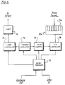
- the system electronics are illustrated in Fig. 2.
- the system electronics are controlled by a microprocessor 40.
- the microprocessor 40 controls a variable oscillator 42 depending on the desired pulse length.
- the variable oscillator 42 feeds both a mirror control 44 and a laser delay counter 46.
- the mirror control 44 drives the mirror 28 via a motor (not shown).
- the mirror 28 is controlled to scan so that a reflected pulse from the laser 16 strikes an element of the radiation-sensitive array 32 dependent upon the range of the reflecting object.
- the microprocessor 40 communicates an appropriate delay to the laser delay counter 46. In this way, each laser pulse will be offset from the mirror scan by a required amount so as to effectuate a scan of the desired range from the system.
- a laser controller 48 controls a laser driver (not shown), for driving the laser diode 16 in the desired pulsed manner.
- the laser controller 48 receives an enable input from a readout controller 50 so that a new set of pulses is not generated from the laser diode 16 until data from the previous set of pulses is readout from the radiation-sensitive array 32.
- the laser controller 48 While basic pulse generation information is received from the variable oscillator 42, the laser controller 48 is connected to the microprocessor 40 for changing various parameters, including the number of pulses to be included in a pulse set, and for sending data to the microprocessor 40, such as when the set of pulses has been completed so that the radiation-sensitive array 32 can be readout.
- the readout controller 50 controls a CCD controller 52, which actually reads the data out of the radiation-sensitive array 32.
- Generation of the enable signal is based on a signal from the laser controller 48 or an internal clock.
- the readout controller 50 can be connected directly to the laser controller 48 for receiving a signal indicative of the beginning or the end of a set of pulses. Such a readout controller 50 would have an internal counter for counting an appropriate delay before sending a signal to the CCD controller 52 to readout the radiation-sensitive array 32.
- data read out from each pixel 34 of the radiation-sensitive array 32 is forwarded to the microprocessor 40, which determines the distance of any object(s) detected by the system based upon the stored charge from each pixel.
- each pixel 34 in the radiation-sensitive array 32 corresponds to a certain distance or distance range from the system. Also as discussed above, by changing the relationship between the pulses and the scanning, each pixel can then represent a different distance or distance range. This permits a very accurate measurement of a distance to a previously unknown object at nearly any range from the system to be determined in minimum time by using a variety of synchronizations between the mirror and the laser pulses.
- the range of a known object can be updated in a fraction of a second with a new set of pulses, and update data can be used to calculate velocity.
- range can be determined to the sub-pixel level based on the data readout from the radiation-sensitive array 32.
- the system can be designed or programmed so that multiple return pulses from a single object fall on more than one pixel. This permits the use of the known algorithms to determine the multiple pulse centroid and thus provide intra-pixel resolution.
- the algorithms can accurately determine range to within 1/100th of a pixel, resulting in excellent range resolution.
- the mechanical scanning system of the present invention has been described relative to a bi-static system in which separate transmission and receiving units are utilized. However, as will be further appreciated by those skilled in the art, such a system can be realized using a single optical system which employs a beam splitter.
- a second embodiment of the present invention operates in accordance with the same principals as the first embodiment, except that rather than using relay optics and a moveable mirror to optically scan a radiation-sensitive array, the mirror and relay optics are eliminated and the radiation-sensitive array is electronically scanned in synchronization with each laser pulse.
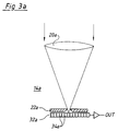
- a first possible aspect of this embodiment is for range-only measurements to a single point. Three different implementations of this aspect of the present invention are illustrated in Figs. 3A, 4A and 5, respectively.
- the transmitting portion of the system is the same as illustrated in Fig. 1 for mechanical scanning, but the receiver portion is different from the receiver 14 of Fig. 1. In receivers 14a-14c of Figs.
- reflected radiation is focused by a lens 20a-20c, passes through a small slit 22a-22c to reject background, and impinges directly onto one (or more) of CCD pixels 34a-34c of CCD arrays 32a-32c.
- the first implementation shown in Fig. 3A uses a simple linear CCD array 32a having n pixels 34a.
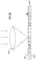
- the receiving lens 20a is focused on the right-most pixel 34a of the left half of the array 32a, designated pixel "n/2" in Fig. 3B.
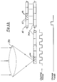
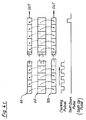
- An appropriate time after the laser source is pulsed, a CCD scan begins towards the right until half of the pixels 34a are scanned. That is, the signal charge stored in each pixel 34a is repeatedly shifted one pixel to the right until half of the pixels 34a have been scanned and the charge originally in the pixel 34a designated "1" is in the pixel 34a designated "n/2 - 1", together with any additional charge received when the charge originally in location "1" was in the focal pixel 34a designated "n/2".
- the pulse will have returned during the CCD scan and the resulting charge from the pulse will reside on one of the pixel(s) in the right half of the CCD array 32a.
- Illustrated in Fig. 3B is the situation where the returning pulse struck the array 32a (and more particularly, the pixel 34a designated "n/2") after approximately two shifts to the right had occurred during a CCD scan.
- the charge from the received pulse mostly resides in the pixel designated "n-2". Since the scanning is continuous and the pulse width will generally be equal to the scan time for a single pixel, received pulses will commonly fall on two consecutive areas as they pass the focal pixel 34a.
- the shift direction is reversed and half the pixels are shifted to the left. This shifting returns the original charges plus any received charge to their original pixels 34a.
- the signal is now stored in the left half of the array 32a, as shown in Fig. 3C, which is the proper position for integrating the next pulse utilizing the above process.
- the CCD array 32a is read out as described for the mechanical approach, again with high SNR.
- a storage area 60 is added to eliminate the inefficiency of reverse shifting for charge accumulation.
- an output register 66 is also added to eliminate the loss of time and/or data during the readout of the array 32b.
- Fig. 4B more fully illustrates the mechanics of electronic scanning using a linear CCD array 32b having a storage area 60.
- the receiving lens 20b is focused on the left-most pixel 34b of the array 32b, which consists of n pixels 34b.
- the contents of each CCD pixel 34b are shifted from left to right, pixel by pixel. This is continued for n clock cycles, after which the shifting is stopped. If an object is in the distance range, the pulse will have returned during the shifting and will have struck one or more of the shifting regions. The resultant signal will reside on the pixel(s) 34b corresponding to the scan clock cycle at which the pulse returned.
- each pixel 34b Upon receiving a command in the form of a storage pulse, the contents of each pixel 34b are shifted into its corresponding position 62 in the storage area 60. The signal amplitude and location in the form of charge 64 are therefore stored, and the system is ready for receiving the next pulse. Since the received pulse has been transferred to the storage area 60, there is no need to shift the array 32b back to its original position, as is the case for the first implementation discussed above. Therefore, additional pulses can be integrated by repeating the above-discussed process without losing time for scanning the charges back to their original positions.
- the optional output CCD register 66 illustrated in Figs. 4A and 4C can be employed to eliminate time lost while reading out.
- the output CCD register 66 is utilized, the stored data from the storage area 60 is transferred when desired to the output register 66 as illustrated by the dashed lines in Fig. 4C.
- the data is read out of each position of the storage register 66 just like it is read out from the CCD array 32 of Fig. 1 and the array 32a of Fig. 3A.
- the data can be read out while the scanning CCD array 32b continues to collect and store new data. Through this process, a duty cycle of 100% is achieved.
- the third implementation of the electronic scanning aspect of the present invention is illustrated in Fig. 5.
- the radiation receiving portion 14c in this implementation is identical to the radiation receiving portion 14a of Fig. 3A and 14b of Fig. 4A, except that the Si CCD array 32c of Fig. 5 has a detector 36 of different wavelength sensitivity bonded to a pixel 34c which lies at the focal point of the lens 20c. Signal data is transferred to the adjoining pixel 34c, where it is electronically shifted across the array 32c in an operation identical to that described for Figs. 3A and 4A.
- the detector 36 can be an infrared detector, which would permit the system to be utilized with infrared radiation, the advantages of which are well known.
- Fig. 6 illustrates a block diagram of the system electronics for the electronic scan system.
- the system electronics required for driving an electronic scanner is slightly different than that for the mechanical scanner.
- the electronic scan system has several advantages over mechanical system, including the elimination of the mirror and necessary calibration, maintenance, etc. associated with mechanical devices. Additionally, due to the nature of the electronic scan system, greater flexibility is possible relative to the mechanical scan system. This flexibility can be provided by a microprocessor 70 which includes memory (not shown) for storing the various control programs for effecting different scans for various distances, ranges and accuracy. Also stored in memory are the above-discussed algorithms for calculating range to the sub-pixel level if so needed. The microprocessor 70, in accordance with one of the stored programs, sets a variable oscillator 72 to a desired frequency.
- the output of the variable oscillator 72 is provided to both a laser controller 74 and a delay counter 76 for the electronic scanning portion of the system.
- the delay counter 76 is also connected to the microprocessor 70 for receiving data regarding the required delay for the scan to be performed. As in the mechanical scanning embodiment, the delay counter 76 provides the required offset between the production of the laser pulses and the scanning, albeit electronic in this embodiment.
- the delayed frequency is then provided to a CCD controller 78 for effecting the scan.
- the laser controller 74 is also connected to the microprocessor 70. Based on the input frequency and instructions from the microprocessor 70, the laser controller 74 causes the laser 16 to output laser pulses having the appropriate pulse width and time interval repetition rate.
- the optics of the radiation transmitter in this embodiment are identical to the receiving optics in the mechanical scanning embodiment.
- the microprocessor 70 also controls the CCD controller 78. Based on the input frequency from the variable oscillator 72 and instructions from the microprocessor 70, the CCD controller 78 scans the CCD arrays 32a-32c in the manner discussed above. Similarly, for the CCD array 32b having the storage area 60, the storage process is controlled in synchronization with each output laser pulse as discussed. At the end of the pulse set or as desired, the CCD controller 78 either causes the stored charges to be shifted from the storage positions 62 back to the respective pixels 34b or causes their transfer to respective positions in the optional storage register 66, depending on the configuration. The CCD controller 78 then causes the data to be read out from either the array 34b or the storage register 66. This data is transferred from the CCD controller 78 to the microprocessor 70 where the distance to the object(s) is calculated and output for further processing or for reading out.
- a mechanical scan must be used with an appropriate CCD or the equivalent so a mechanical scan can be performed using charge transfer properties of CCDs.
- Si technology can be used by bonding an appropriate detector to a Si CCD as shown in Fig. 5.
- Charge transfer and on-chip charge storage increase enormously the flexibility and sensitivity of the charge integration range detector of the present invention. Given current Si CCD technology, this range detector invention becomes signal/background shot noise limited after less than 10 detected photons and can detect and integrate signals of less than one photon per pulse with high efficiency.
- the equivalent range for each pixel is determined by the pixel scan rate and speed of light. Assuming a current maximum rate of 40 x 106 pixels per second, the minimum pixel equivalent range is 3.75 meters, which is twice the range resolution at a SNR of 1.0. At higher SNR and with interpolation, the range resolution is approximately 1.87 meters. Future improvements in CCD technology and enhancements to this invention will improve the performances even further.
- a known method of obtaining a three-dimensional image of an object is to employ a range detector to scan a direction and record the range as a function of direction.
- the composite of range versus direction forms a three-dimensional image of the scene over which the ranger was directed. This is a time consuming process because each picture element of the scene requires an independent range measurement.
- a scene of n x m elements requires an equivalent number of independent measurements.
- the present invention provides a number of faster techniques by which three-dimensional information can be obtained.
- a fan-shaped or slit radiation pulse can be used in combination with a two-dimensional CCD array.
- an object area is "illuminated” incrementally step-by-step by a series of fan-shaped pulses until the entire area has been illuminated.
- the returning radiation from each pulse is scanned over a respective linear portion of the two-dimensional array. After the entire object area has been ranged, the two-dimensional CCD array will contain an image of an object in the object area.
- Another aspect of the electrical scanning embodiment of the present invention provides an improved three-dimensional imaging technique which is accurate and even faster. Rather than the focused image directly striking one of the pixels in a CCD array, an optical transfer is employed which maps an imaged two-dimensional scene to a linear CCD, as illustrated in Fig. 7. With this enhancement, a three-dimensional image of an object is formed with a single measurement, given a sufficient number of photons are received from the single pulse.
- the transmission optics are the same as previously described, except that the optics must illuminate the desired scene, as opposed to the above-described rangers, in which a single spot can be illuminated.
- the receiver 14d must be adapted so that an object area (scene) is imaged, with the imaged area being transferrable and readable. This is accomplished by forming a two-dimensional imaging surface 90, which is positioned not at the focal point of a receiving lens 20d, but at a focal plane generally parallel to the lens 20d so that reflected photons from the pulse will strike the imaging surface 90 dependent upon the point of the object area from which they were reflected.
- the imaging surface 90 is composed of an n x m array comprising open first ends of optical fibers 92. The open end of each optical fiber 92 receives photons from an object via the receiving lens 20d. The received photons from the end of each optical fiber 92 are transferred through each optical fiber 92 to the linear CCD array 32d.
- Each optical fiber 92 has a like predetermined number of pixels 34d which are dedicated exclusively to it.
- the second ends of the fibers 92 are spaced apart on the array 32d by the predetermined number of pixels and face or are focused on a first of their associated pixels.
- the dedicated location on the array 32d and the focal plane position of each fiber 92 are thus known.
- each fiber 92 can have a large number of pixels 34d associated therewith at the dedicated location on the array 32d. However, in practice, this would result in very long read out times for the array 32d. Accordingly, the mean range to the scene of interest is assumed known by a prior range measurement, so the depth of the object area is minimized, as is the number of pixels for each fiber 92.
- a laser pulse is generated and the CCD scan is delayed for the appropriate scene range.
- the CCD scan is started just prior to the arrival of the return pulse from the scene.
- the CCD array 32d is scanned (left to right in Fig. 7) only by the number of pixels dedicated to the individual fibers 92, which is a constant.
- the scanning is stopped after the number of pixels 34d dedicated to each fiber 92 have been scanned.
- the pulse will return from any object in the scene area.
- the range from points on the surface of the object to their associated fibers 92 on the array 90 is dependent upon the time of arrival at each optical fiber 92, as recorded by the signal location in the CCD array 32d.
- each fiber 92 on both the surface of the array 90 and the CCD array 32d are known, time to each respective point of an object (distance) and location of each respective point are stored in the CCD array 32d.
- a first pixel associated with the first fiber 92 will store a signal
- the second or third pixel associated with the second fiber 92 will store a signal.
- a plurality of such pulses can be scanned and received for low noise integration within the detector as previously described for higher SNR or lower laser power prior to readout.
- Horizontal and vertical scene information is obtained by reconstruction of the signals from the known location of fibers 92 in the focal plane. Relative distance to each element of the image is obtained by computing the number of CCD elements separating the respective fiber signals.
- Fig. 8 illustrates this process.
- Fig. 8 illustrates the range to a linear portion of an object 94 as received by a portion of the CCD array 32d via a row r1 of the array 90.
- the row r1 of the array 90 comprises ten optical fibers 92, designated f1-f10.
- Each of the ten optical fibers f1-f10 detects data relative to the range of each of ten separate points p1-p10 on the surface of the object 94.
- Each optical fiber f1-f10 has three pixels 34d in the CCD array 32d associated therewith, and each fiber is focused on the left-most pixel in its set of three pixels.
- the location of the returned signal in the three pixels 34d associated with each fiber f1-f10 will being indicative of the distance between each point p1-p10 and the end of each optic fiber f1-f10 on the surface of the array 90.
- the first signal from the pulse received by the array 90 is from point p10.
- signal s10 from point p10 will be found in the third pixel associated with fiber f10, indicating that the signal s10 was received early in the scan and that point p10 of the object 94 is close relative to the depth of the scene being scanned.
- the distance to point p10 will be known because of the location of signal s10 in the three pixels associated with fiber f10.
- range to point p10 to within a fraction of the distance range represented by the third pixel can be determined by the use of pulse integration and the known algorithms to provide intra-pixel resolution.
- the last signal from the pulse received by the fibers f1-f10 is from the point p1 on the object 94, and is received by the fiber f1 and stored in the first pixel 34d associate shape of the fiber f1.
- the distance to each point p1-p10 can be determined.
- the shape of the surface of the object 94 from point p1 to point p10 can be determined through interpolation. By combining distance data relative to each fiber, the shape of the surface of the object 94 can be determined.
- the microprocessor 70 reads out the CCD array 32d via the CCD controller 78.
- Memory (not shown) associated with the microprocessor 70 already has data regarding the range represented by each pixel in each pixel set represents the order in which the pixel sets are read out from the CCD array 32d, and any resolution algorithm to be employed. Based on this stored data and the location of each stored charge relative to the other stored charges being read out, relative range from each fiber can be determined.
- a single CCD array or a CCD array corresponding to each row of the array 90 can be employed.
- the z axis data (distance) to each point on the object 94 is obtained as described above by determining the distance between each point on the array 90 and its corresponding point on the object 94.
- the x and y axes data for each point are known from the location of each optical fiber 92 on the array 90 and its known feed location on the CCD array(s) 32d.
- a 5000 element CCD array with fiber separation of five pixels provides a 1000 element image of the scene. More points on the object can be imaged by using a larger CCD array or multiple CCD arrays that are suitably large.
- the range interval for the three-dimensional image is controllable by varying the CCD scan rate.
- a three-dimensional image of an object can be formed with a single measurement with the above-discussed system.
- the sensitivity and range resolution for obtaining three-dimensional object information are the same as for ranging.
- the laser power or number of pulses must be increased for equivalent SNR because a larger area is being irradiated.
Landscapes
- Physics & Mathematics (AREA)
- Engineering & Computer Science (AREA)
- Electromagnetism (AREA)
- Computer Networks & Wireless Communication (AREA)
- General Physics & Mathematics (AREA)
- Radar, Positioning & Navigation (AREA)
- Remote Sensing (AREA)
- Optical Radar Systems And Details Thereof (AREA)
- Length Measuring Devices By Optical Means (AREA)
- Measurement Of Optical Distance (AREA)
- Transforming Light Signals Into Electric Signals (AREA)
Applications Claiming Priority (2)
| Application Number | Priority Date | Filing Date | Title |
|---|---|---|---|
| US07/551,887 US5056914A (en) | 1990-07-12 | 1990-07-12 | Charge integration range detector |
| US551887 | 1990-07-12 |
Publications (1)
| Publication Number | Publication Date |
|---|---|
| EP0465806A2 true EP0465806A2 (fr) | 1992-01-15 |
Family
ID=24203086
Family Applications (1)
| Application Number | Title | Priority Date | Filing Date |
|---|---|---|---|
| EP91108460A Withdrawn EP0465806A2 (fr) | 1990-07-12 | 1991-05-24 | Détecteur de distances à intégration de charges |
Country Status (3)
| Country | Link |
|---|---|
| US (1) | US5056914A (fr) |
| EP (1) | EP0465806A2 (fr) |
| JP (1) | JPH05100028A (fr) |
Cited By (8)
| Publication number | Priority date | Publication date | Assignee | Title |
|---|---|---|---|---|
| WO1999026083A1 (fr) * | 1997-11-13 | 1999-05-27 | 3Dv Systems Ltd. | Imagerie tridimensionnelle par triangulation a double longueur d'onde |
| WO1999034235A1 (fr) * | 1997-12-23 | 1999-07-08 | Siemens Aktiengesellschaft | Procede et dispositif pour la prise d'une vue tridimensionnelle permettant la mesure d'une distance |
| US6057909A (en) * | 1995-06-22 | 2000-05-02 | 3Dv Systems Ltd. | Optical ranging camera |
| US6100517A (en) * | 1995-06-22 | 2000-08-08 | 3Dv Systems Ltd. | Three dimensional camera |
| US6445884B1 (en) | 1995-06-22 | 2002-09-03 | 3Dv Systems, Ltd. | Camera with through-the-lens lighting |
| DE10158967A1 (de) * | 2001-11-30 | 2003-06-12 | Conti Temic Microelectronic | Verfahren zur optischen Entfernungsmessung in Fahrzeugen |
| EP1191306A3 (fr) * | 2000-09-26 | 2004-12-15 | Fuji Photo Film Co., Ltd. | Méthode et dispositif de mesure de distance |
| WO2026032496A1 (fr) | 2024-08-06 | 2026-02-12 | Fr-Innovations Gmbh | Caméra amovible dotée d'une source de lumière, et utilisation de ladite caméra amovible en sylviculture |
Families Citing this family (40)
| Publication number | Priority date | Publication date | Assignee | Title |
|---|---|---|---|---|
| US5193120A (en) * | 1991-02-27 | 1993-03-09 | Mechanical Technology Incorporated | Machine vision three dimensional profiling system |
| DE4106892A1 (de) * | 1991-03-05 | 1992-09-10 | Zeiss Carl Fa | Verfahren und vorrichtung zum messen von entfernungen |
| US5257085A (en) * | 1991-04-24 | 1993-10-26 | Kaman Aerospace Corporation | Spectrally dispersive imaging lidar system |
| US5293162A (en) * | 1992-03-09 | 1994-03-08 | Bachalo William D | Laser based tracking device for detecting the distance between a vehicle and a roadway marker |
| US5434612A (en) * | 1992-09-25 | 1995-07-18 | The United States Of America As Represented By The Secretary Of The Army | Duo-frame normalization technique |
| JP3518891B2 (ja) * | 1994-05-27 | 2004-04-12 | オリンパス株式会社 | カメラの測距装置、カメラの移動体検出方法及びカメラ |
| DE4422886C2 (de) * | 1994-06-30 | 1997-02-20 | Daimler Benz Aerospace Ag | Verfahren und Einrichtung zur optischen Bestimmung räumlicher Positionen einzelner reflektierender Objekte |
| JPH0886641A (ja) * | 1994-09-16 | 1996-04-02 | Olympus Optical Co Ltd | 投受光式焦点検出装置 |
| US5703639A (en) * | 1994-10-25 | 1997-12-30 | Dalsa, Inc. | Charge coupled device pulse discriminator |
| US5682229A (en) * | 1995-04-14 | 1997-10-28 | Schwartz Electro-Optics, Inc. | Laser range camera |
| US5892575A (en) * | 1996-05-10 | 1999-04-06 | Massachusetts Institute Of Technology | Method and apparatus for imaging a scene using a light detector operating in non-linear geiger-mode |
| US5889582A (en) * | 1997-03-10 | 1999-03-30 | Virtek Vision Corporation | Image-directed active range finding system |
| EP0893704A2 (fr) * | 1997-07-25 | 1999-01-27 | TRW Inc. | Système d'imagerie avec filtre optique pour rayonnement laser dispersé |
| FR2769450B1 (fr) * | 1997-10-03 | 2000-01-14 | Matra Marconi Space France | Dispositif photosensible a couplage et accumulation de charges et lidar incorporant un tel dispositif |
| US5953110A (en) * | 1998-04-23 | 1999-09-14 | H.N. Burns Engineering Corporation | Multichannel laser radar |
| US6867808B1 (en) | 1999-03-19 | 2005-03-15 | Scott T. Boden | Time domain imager |
| FR2803159B1 (fr) * | 1999-12-24 | 2002-03-08 | Matra Marconi Space France | Dispositif photosensible a accumulation de charges et lidar incorporant un tel dispositif |
| US7087886B2 (en) * | 2000-05-09 | 2006-08-08 | El-Op Electro-Optics Industries Ltd. | Method and a system for multi-pixel ranging of a scene |
| US6639684B1 (en) * | 2000-09-13 | 2003-10-28 | Nextengine, Inc. | Digitizer using intensity gradient to image features of three-dimensional objects |
| DE10117147A1 (de) * | 2001-04-05 | 2002-10-10 | Bodenseewerk Geraetetech | Dual-Mode-Suchkopf |
| US6507392B1 (en) | 2001-04-16 | 2003-01-14 | Bae Systems Information And Electronic Systems Integration Inc. | Single multiple aperture (“SMART”) lens system |
| US6943873B2 (en) * | 2001-07-17 | 2005-09-13 | Bae Systems Integrated Defense Solutions Inc. | Fiber optical laser detection and ranging system |
| US6924887B2 (en) * | 2002-03-27 | 2005-08-02 | Sarnoff Corporation | Method and apparatus for generating charge from a light pulse |
| US6657706B2 (en) * | 2002-03-27 | 2003-12-02 | Sarnoff Corporation | Method and apparatus for resolving relative times-of-arrival of light pulses |
| US9007197B2 (en) | 2002-05-20 | 2015-04-14 | Intelligent Technologies International, Inc. | Vehicular anticipatory sensor system |
| US7098999B1 (en) * | 2004-03-05 | 2006-08-29 | Raytheon Company | High-speed readout circuit and system incorporating same |
| US7711179B2 (en) | 2004-04-21 | 2010-05-04 | Nextengine, Inc. | Hand held portable three dimensional scanner |
| US7995834B1 (en) | 2006-01-20 | 2011-08-09 | Nextengine, Inc. | Multiple laser scanner |
| US7995191B1 (en) * | 2006-06-29 | 2011-08-09 | Sandia Corporation | Scannerless laser range imaging using loss modulation |
| DE102008031682A1 (de) * | 2008-07-04 | 2010-03-11 | Eads Deutschland Gmbh | Direktempfang-Doppler-LIDAR-Verfahren und Direktempfang-Doppler-LIDAR-Vorrichtung |
| DE102008032216A1 (de) * | 2008-07-09 | 2010-01-14 | Sick Ag | Vorrichtung zur Erkennung der Anwesenheit eines Objekts im Raum |
| JP5765698B2 (ja) * | 2010-03-31 | 2015-08-19 | 北陽電機株式会社 | マルチ信号処理装置、測距装置、及びマルチ測距システム |
| CN102095406B (zh) * | 2010-12-16 | 2012-05-09 | 哈尔滨工程大学 | 一种摄像机与激光结合的光学测距方法 |
| RU2692121C2 (ru) * | 2013-03-05 | 2019-06-21 | Общество с ограниченной ответственностью "Центр исследований и разработок концерна Агат" | Способ лидарного зондирования и устройство для его осуществления |
| US10502618B2 (en) * | 2016-12-03 | 2019-12-10 | Waymo Llc | Waveguide diffuser for light detection using an aperture |
| CN118714460A (zh) * | 2016-12-15 | 2024-09-27 | 松下知识产权经营株式会社 | 摄像装置、摄像方法及计算机程序产品 |
| EP3392674A1 (fr) * | 2017-04-23 | 2018-10-24 | Xenomatix NV | Structure de pixels |
| WO2019014494A1 (fr) * | 2017-07-13 | 2019-01-17 | Apple Inc. | Comptage d'impulsions précoce-retardées pour capteurs de profondeur émettant de la lumière |
| US12356740B2 (en) | 2020-09-25 | 2025-07-08 | Apple Inc. | Transistor integration with stacked single-photon avalanche diode (SPAD) pixel arrays |
| CN112394363B (zh) * | 2020-10-21 | 2023-12-12 | 深圳奥锐达科技有限公司 | 一种多线扫描距离测量系统 |
Family Cites Families (13)
| Publication number | Priority date | Publication date | Assignee | Title |
|---|---|---|---|---|
| US4707698A (en) * | 1976-03-04 | 1987-11-17 | Constant James N | Coordinate measurement and radar device using image scanner |
| US4277167A (en) * | 1976-08-25 | 1981-07-07 | The United States Of America As Represented By The Secretary Of The Navy | Depth mapping system |
| US4380391A (en) * | 1980-09-30 | 1983-04-19 | The United States Of America As Represented By The Secretary Of The Army | Short pulse CO2 laser for ranging and target identification |
| JPS5810605A (ja) * | 1981-07-10 | 1983-01-21 | Canon Inc | 距離測定装置 |
| US4611912A (en) * | 1983-04-04 | 1986-09-16 | Ball Corporation | Method and apparatus for optically measuring distance and velocity |
| US4594000A (en) * | 1983-04-04 | 1986-06-10 | Ball Corporation | Method and apparatus for optically measuring distance and velocity |
| JPS6020111A (ja) * | 1983-07-14 | 1985-02-01 | Fuji Electric Corp Res & Dev Ltd | 距離測定装置 |
| DE3404396A1 (de) * | 1984-02-08 | 1985-08-14 | Dornier Gmbh, 7990 Friedrichshafen | Vorrichtung und verfahren zur aufnahme von entfernungsbildern |
| US4627722A (en) * | 1984-08-31 | 1986-12-09 | Ball Corporation | Method and apparatus for optically measuring three-dimensional coordinates |
| JPS61116611A (ja) * | 1984-11-12 | 1986-06-04 | Canon Inc | 距離測定方法 |
| US4794262A (en) * | 1985-12-03 | 1988-12-27 | Yukio Sato | Method and apparatus for measuring profile of three-dimensional object |
| US4774403A (en) * | 1987-03-30 | 1988-09-27 | Harvey Industries, Inc. | Triangulation-type position measuring device |
| US4830485A (en) * | 1987-11-23 | 1989-05-16 | General Electric Company | Coded aperture light detector for three dimensional camera |
-
1990
- 1990-07-12 US US07/551,887 patent/US5056914A/en not_active Expired - Fee Related
-
1991
- 1991-05-24 EP EP91108460A patent/EP0465806A2/fr not_active Withdrawn
- 1991-07-12 JP JP3197329A patent/JPH05100028A/ja active Pending
Cited By (15)
| Publication number | Priority date | Publication date | Assignee | Title |
|---|---|---|---|---|
| US6445884B1 (en) | 1995-06-22 | 2002-09-03 | 3Dv Systems, Ltd. | Camera with through-the-lens lighting |
| US6057909A (en) * | 1995-06-22 | 2000-05-02 | 3Dv Systems Ltd. | Optical ranging camera |
| US6091905A (en) * | 1995-06-22 | 2000-07-18 | 3Dv Systems, Ltd | Telecentric 3D camera and method |
| US6100517A (en) * | 1995-06-22 | 2000-08-08 | 3Dv Systems Ltd. | Three dimensional camera |
| CN100524015C (zh) * | 1995-06-22 | 2009-08-05 | 3Dv系统有限公司 | 生成距景物距离的图象的方法和装置 |
| US6654556B2 (en) | 1995-06-22 | 2003-11-25 | 3Dv Systems Ltd. | Camera with through-the-lens lighting |
| WO1999026083A1 (fr) * | 1997-11-13 | 1999-05-27 | 3Dv Systems Ltd. | Imagerie tridimensionnelle par triangulation a double longueur d'onde |
| US6373557B1 (en) | 1997-12-23 | 2002-04-16 | Siemens Aktiengesellschaft | Method and apparatus for picking up a three-dimensional range image |
| WO1999034235A1 (fr) * | 1997-12-23 | 1999-07-08 | Siemens Aktiengesellschaft | Procede et dispositif pour la prise d'une vue tridimensionnelle permettant la mesure d'une distance |
| US6993255B2 (en) | 1999-02-16 | 2006-01-31 | 3Dv Systems, Ltd. | Method and apparatus for providing adaptive illumination |
| US7355648B1 (en) | 1999-02-16 | 2008-04-08 | 3Dv Systems Ltd. | Camera having a through the lens pixel illuminator |
| EP1191306A3 (fr) * | 2000-09-26 | 2004-12-15 | Fuji Photo Film Co., Ltd. | Méthode et dispositif de mesure de distance |
| DE10158967A1 (de) * | 2001-11-30 | 2003-06-12 | Conti Temic Microelectronic | Verfahren zur optischen Entfernungsmessung in Fahrzeugen |
| WO2003048805A3 (fr) * | 2001-11-30 | 2003-09-04 | Conti Temic Microelectronic | Procede de mesure optique des distances dans un vehicule |
| WO2026032496A1 (fr) | 2024-08-06 | 2026-02-12 | Fr-Innovations Gmbh | Caméra amovible dotée d'une source de lumière, et utilisation de ladite caméra amovible en sylviculture |
Also Published As
| Publication number | Publication date |
|---|---|
| US5056914A (en) | 1991-10-15 |
| JPH05100028A (ja) | 1993-04-23 |
Similar Documents
| Publication | Publication Date | Title |
|---|---|---|
| US5056914A (en) | Charge integration range detector | |
| US5006721A (en) | Lidar scanning system | |
| US3781111A (en) | Short range laser obstacle detector | |
| US11408983B2 (en) | Lidar 2D receiver array architecture | |
| US7834985B2 (en) | Surface profile measurement | |
| US5309212A (en) | Scanning rangefinder with range to frequency conversion | |
| US11796642B2 (en) | Oversamplng and transmitter shooting pattern for light detection and ranging (LIDAR) system | |
| US6535275B2 (en) | High resolution 3-D imaging range finder | |
| US5900611A (en) | Laser scanner with integral distance measurement system | |
| US4967270A (en) | Lidar system incorporating multiple cameras for obtaining a plurality of subimages | |
| US20010046317A1 (en) | Three-dimensional measurement device and three-dimensional measurement method | |
| US4226529A (en) | Viewing systems | |
| US5015868A (en) | Real time distance sensor | |
| JP2004538491A (ja) | 三次元距離画像を記録するための方法及び装置 | |
| US6480265B2 (en) | Active target distance measurement | |
| FR2677834A1 (fr) | Systeme d'imagerie laser a barrette detectrice. | |
| US20200158832A1 (en) | Muilti-detector with interleaved photodetector arrays and analog readout circuits for lidar reciever | |
| CA1295039C (fr) | Systeme galvanometrique de balayage optique | |
| US5724123A (en) | Distance measuring equipment for detecting a scanning direction | |
| US4622462A (en) | Method and apparatus for three-dimensional scanning | |
| FR2476325A1 (fr) | Systeme de reperage omnidirectionnel pour objets en mouvement | |
| US4119379A (en) | Optical detection and ranging apparatus | |
| US5847833A (en) | Distance measuring method and distance measuring apparatus | |
| US4853541A (en) | Device for detecting the spatial orientation of excessively heated points | |
| US5790241A (en) | Laser rangefinder |
Legal Events
| Date | Code | Title | Description |
|---|---|---|---|
| PUAI | Public reference made under article 153(3) epc to a published international application that has entered the european phase |
Free format text: ORIGINAL CODE: 0009012 |
|
| AK | Designated contracting states |
Kind code of ref document: A2 Designated state(s): AT BE CH DE DK ES FR GB GR IT LI LU NL SE |
|
| 17P | Request for examination filed |
Effective date: 19921113 |
|
| STAA | Information on the status of an ep patent application or granted ep patent |
Free format text: STATUS: THE APPLICATION HAS BEEN WITHDRAWN |
|
| 18W | Application withdrawn |
Withdrawal date: 19930120 |
|
| R18W | Application withdrawn (corrected) |
Effective date: 19930120 |