EP0466487A2 - Autorisation d'un mode de test dans un module électronique avec un nombre limité des broches de contact - Google Patents
Autorisation d'un mode de test dans un module électronique avec un nombre limité des broches de contact Download PDFInfo
- Publication number
- EP0466487A2 EP0466487A2 EP91306300A EP91306300A EP0466487A2 EP 0466487 A2 EP0466487 A2 EP 0466487A2 EP 91306300 A EP91306300 A EP 91306300A EP 91306300 A EP91306300 A EP 91306300A EP 0466487 A2 EP0466487 A2 EP 0466487A2
- Authority
- EP
- European Patent Office
- Prior art keywords
- output
- current
- output transistor
- test
- level
- Prior art date
- Legal status (The legal status is an assumption and is not a legal conclusion. Google has not performed a legal analysis and makes no representation as to the accuracy of the status listed.)
- Withdrawn
Links
- 238000012360 testing method Methods 0.000 title claims abstract description 56
- 230000002159 abnormal effect Effects 0.000 claims abstract description 9
- 230000000977 initiatory effect Effects 0.000 claims description 9
- 238000001514 detection method Methods 0.000 claims description 6
- 238000011990 functional testing Methods 0.000 claims description 5
- 238000000034 method Methods 0.000 abstract description 7
- 230000001976 improved effect Effects 0.000 description 4
- 230000001939 inductive effect Effects 0.000 description 3
- 230000004044 response Effects 0.000 description 3
- 230000004075 alteration Effects 0.000 description 2
- 238000012986 modification Methods 0.000 description 2
- 230000004048 modification Effects 0.000 description 2
- 230000008859 change Effects 0.000 description 1
- 238000007796 conventional method Methods 0.000 description 1
- 230000007812 deficiency Effects 0.000 description 1
- 238000010586 diagram Methods 0.000 description 1
- 230000000630 rising effect Effects 0.000 description 1
- 230000011664 signaling Effects 0.000 description 1
- 230000001960 triggered effect Effects 0.000 description 1
- 238000004804 winding Methods 0.000 description 1
Images
Classifications
-
- G—PHYSICS
- G01—MEASURING; TESTING
- G01R—MEASURING ELECTRIC VARIABLES; MEASURING MAGNETIC VARIABLES
- G01R31/00—Arrangements for testing electric properties; Arrangements for locating electric faults; Arrangements for electrical testing characterised by what is being tested not provided for elsewhere
- G01R31/28—Testing of electronic circuits, e.g. by signal tracer
- G01R31/317—Testing of digital circuits
- G01R31/31701—Arrangements for setting the Unit Under Test [UUT] in a test mode
-
- G—PHYSICS
- G01—MEASURING; TESTING
- G01R—MEASURING ELECTRIC VARIABLES; MEASURING MAGNETIC VARIABLES
- G01R31/00—Arrangements for testing electric properties; Arrangements for locating electric faults; Arrangements for electrical testing characterised by what is being tested not provided for elsewhere
- G01R31/28—Testing of electronic circuits, e.g. by signal tracer
- G01R31/2851—Testing of integrated circuits [IC]
- G01R31/2884—Testing of integrated circuits [IC] using dedicated test connectors, test elements or test circuits on the IC under test
Definitions
- This invention is directed to a technique and apparatus for selectively putting an IC (integrated circuit), or another type of electronic module, into a test mode in which one or more functions of the IC or module can be tested for proper operation.
- IC integrated circuit
- a single-chip voltage regulator is an example of an IC to which this invention is particularly well suited.
- electronic module means an IC or other form of packaged electronic circuitry having a limited number of input/output pins.
- an electronic module be able to enter a test mode, in which one or more functional characteristics of the module are tested and/or modified. This can be done by including a separate pin which receives a signal for initiating the test mode. But where a pin cannot be dedicated solely to the testing function (particularly in IC′s) the test mode has been conventionally initiated by applying to a pin, which pin is also used for a function other than testing, a voltage which is outside its normal operating range (typically above V cc or below ground). That voltage is detected in the module and used to trigger the test mode.
- an automotive voltage regulator that is constructed as an IC may have only three input/output pins that are available for normal operation of the device and for use in initiating the test mode.
- the environment in which the voltage regulator is used in sometimes too noisy to reliably use an abnormally high or low voltage on one of the pins to initiate the test mode.
- the invention provides an electronic module capable of being selectively put into a test mode, comprising: an output transistor having an output terminal; a signal output pin coupled to the output terminal; fault detection circuitry sensing the operation of the output transistor for causing the level of current in the output transistor to be at least reduced when the output transistor experiences an abnormal signal level; means responsive to the fault detection circuitry causing the level of current in the output transistor to be reduced for developing a test-mode signal; and means responsive to the test mode signal for initiating a functional test of the module, whereby the module can be put into the test mode by intentionally establishing a condition at the output pin that causes the output transistor to experience an abnormal signal level.
- the invention provides a single-chip automotive voltage regulator IC having only three input/output pins, one of the pins being adapted to receive battery voltage, another of the pins being adapted to receive a reference potential, and the third pin being an output pin adapted to deliver an output current to an alternator, the regulator comprising: an output transistor coupled to the output pin for delivering the output current thereto; an over-current detector sensing the level of current in the output transistor and developing an output signal upon sensing that the level of current exceeds a selected threshold; control circuitry coupled to the over-current detector and to the output transistor for at least reducing the level of current in the output transistor responsive to the over-current detector sensing a level of current that exceeds the threshold; and circuitry responsive to said output signal for generating a test-mode signal; and test circuitry responsive to the test mode signal for initiating a preselected functional test of the voltage regulator.
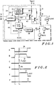
- a form of electronic module is shown which incorporates various aspects of the invention to provide on improved voltage regulator IC 10 whose boundary is shown by the dashed line.
- Various aspects of the invention are applicable to other forms of electronic modules.
- the illustrated embodiment has only three input/output pins: a first pin 12 that receives battery voltage V batt from the battery of a vehicle that uses the IC regulator 10; a second pin 14 that receives a reference potential (such as ground) for use by the circuitry within the IC regulator 10; and a third pin 16 which carries output current to a load which, in the case of this particular embodiment, is the field winding of an alternator (not shown).
- an output transistor Q1 has an output terminal 18 coupled to the output pin 16.
- the emitter of Q1 is coupled through a resistor 20 to the battery terminal 12. With this conventional arrangement, the transistor Q1 supplies load current to the alternator via the output pin 16.
- a conventional control circuit 22 that, in the normal (non-test) mode of operation, senses the value of an internal voltage source V ref1 , senses the value of the battery voltage via a lead 24, and controls the level of current in the transistor Q1 based on the difference in the values of the sensed voltages.
- a conventional fault detector shown here as an over-current detector 26, is included.
- the purpose of this device is to sense the level of current in the transistor Q1, and to at least reduce that current level when a threshold level of current has been exceeded.
- the detector 26 may accomplish this by sensing the voltage drop across the resistor 20 and, when the sensed voltage is too high, sending a signal to the control circuit 22 via a lead 28.
- the control circuit 22 may respond to the received signal by either reducing the level of current in the transistor Q1 to a relatively low level, or by shutting off the transistor Q1 entirely.
- the detector 26 may include a direct connection back to the transistor Q1 to shut it down, thereby overriding the control normally executed by the control circuit 22. In either case, the detector 26 senses when the transistor Q1 conducts an abnormally high level of current and causes (either directly or indirectly) the level of current in Q1 to be at least reduced, and possibly shut off completely.
- an abnormal signal level is established at the output pin 16 so as to enable (trigger) the detector 26.
- the enablement of the detector 26 is sensed and that is used to initiate the test mode.
- an abnormal signal level is established at the output pin 16, preferably be inducing an abnormally high current pulse therein. This may be accomplished by removing the normal load from the pin 16 and switching in a low impedance test load which will cause the current through Q1 to exceed the detect threshold of the detector 26.
- Waveform C of Fig. 2 illustrates such an abnormal current pulse. (The waveforms A-F in Fig. 2 appear on leads in Fig. 1 which carry the same letter designation.)
- the detector 26 responds by signaling the control circuit 22, via lead 28, that an abnormally high current condition has been detected. This causes the control circuit 22 to change the base drive to the transistor Q1 via a lead 30. As shown by waveform A of Fig. 2, the voltage applied to the base of Q1 by the control circuit 22 previously dropped to a low voltage at time t1 to start a normal cycle of operation. This resulted in the voltage at the output terminal 18 of Q1 rising, as shown by waveform B. Thus, between times t1 and t2, the IC 10 operates normally; i.e., in a nontest mode.
- the current pulse shown in waveform C occurs and the output voltage from the control 22 (waveform A) goes high to turn off the transistor Q1 (alternate embodiments may merely reduce the level of current in Q1 to a low, safe value). This drives the voltage at terminal 18 low at time t2 (waveform B).
- the detector 26 has another output lead 32 which carries a pulse 36 (waveform D) to a flip-flop 34.
- the illustrated pulse 36 is generated when the detector 26 senses the abnormally high current level in the transistor Q1.
- the flip-flop 34 can develop an output signal that has one of two states, high and low. When triggered by the pulse 36, the flip-flop 34 generates a high output state which constitutes a test-mode signal 37. See waveform E in Fig. 2. The existence of this signal 37 indicates that a test mode is now being initiated in the IC 10.
- the test mode signal 37 is coupled to a switch 38 that moves a switch contact 40 from the present illustrated position where it couples V ref1 to the control 22 to the other illustrated position where it couples V ref2 to the control 22.
- a new reference voltage source is coupled to one of the inputs of the control circuit 22 so that the value of that reference voltage maybe compared to the battery voltage received via the terminal 12 and lead 24.
- control circuit 22 will now output a signal to the base of the transistor Q1 so that its output current, which is indicative of the test results, may now be monitored at the output terminal 16, thereby to sense the results of the test.
- the testing involves substituting the reference voltage source V ref2 in place of the reference voltage source V ref1 as an example of how the invention might be used to implement a test.
- V ref1 would be the normal reference voltage against which the battery voltage would be compared by the control circuit 22, and the V ref1 would typically have a temperature coefficient of minus 10 millivolts per degree centigrade at 14 volts
- V ref2 would preferably have a temperature coefficient of zero degrees millivolts per degree centigrade so that the comparison between the battery voltage and the reference voltage V ref2 can be conducted, irrespective of the temperature of the IC 10.
- other and/or different tests may be conducted in response to the test mode signal, such as by changing the frequency of the operation of the IC 10.
- a different type of test can be conducted that is specific to the needs of the particular electronic module.
- the test illustrated in connection with Fig. 1 is merely exemplary of one of many such tests which may be conducted.
- the transistor Q1 outputs a low level current (during the test mode) that is modulated or controlled by the control circuit 22 to indicate, at the output pin 16, the results of the test.
- the transistor Q1 may be completely shut down and latched off in response to the detection of a abnormally high level of current.
- This alternate mode of operation is shown in Fig. 2 by the dashed lines 39 and 41 (waveforms A and B) which indicate that waveform A may be latched high at the beginning of the test mode, thereby latching waveform B low and holding the transistor Q1 completely off.
- another transistor Q2 is preferably included.
- the transistor Q2 constitutes a second output transistor which is coupled to the output pin 16 in parallel with the other output transistor Q1.
- the transistor Q2 will be capable of conducting only a small fraction of the current that the transistor Q1 is capable of conducting, and the transistor Q2 will not be shut off when the detector 26 detects that the transistor Q1 is conducting an abnormally high level of current.
- the transistor Q2 is held in an on condition specifically for the purpose of supplying a low level output current to the output pin 16 under the control of control circuitry 22 during the test mode operation.
- the base drive of the transistor Q2 is received from the control circuit 22 via a separate lead 42 which does not carry a shut-down signal in response to over-current detection.
- the lead 42 merely carries test mode information from the control circuit 22 so that a signal is available at output pin 16 to represent the test results while the transistor Q1 is completely shut down.
- the flip-flop 34 has an input lead 44 that receives a reset signal in order to periodically insure that the output of the flip-flop 34 is in the normal, i.e. non-test mode, state.
- a reset signal can be derived from a conventional POR (power on reset) signal as is conventionally available in IC′s, or it can alternately be received from the control circuit 22 via a lead shown as a dashed line 46.
- the illustrated embodiment provides an electronic module with the capability of using some circuitry which is conventionally included within an electronic module in a manner so as to easily and economically implement a test mode operation without increasing the number of input/output pins that are required.
- the preferred method of inducing the test mode operation i.e., inducing an abnormally high level of current at the output pin 16 makes this test mode technique useable in high noise environments in which merely raising or lowering the voltage at one of the input/output pins beyond its normal range would not be a reliable indication that the test mode should be initiated.
Landscapes
- Engineering & Computer Science (AREA)
- General Engineering & Computer Science (AREA)
- Physics & Mathematics (AREA)
- General Physics & Mathematics (AREA)
- Computer Hardware Design (AREA)
- Microelectronics & Electronic Packaging (AREA)
- Continuous-Control Power Sources That Use Transistors (AREA)
Applications Claiming Priority (2)
| Application Number | Priority Date | Filing Date | Title |
|---|---|---|---|
| US553469 | 1990-07-13 | ||
| US07/553,469 US5126659A (en) | 1990-07-13 | 1990-07-13 | Enablement of a test mode in an electronic module with limited pin-outs |
Publications (2)
| Publication Number | Publication Date |
|---|---|
| EP0466487A2 true EP0466487A2 (fr) | 1992-01-15 |
| EP0466487A3 EP0466487A3 (en) | 1992-04-01 |
Family
ID=24209528
Family Applications (1)
| Application Number | Title | Priority Date | Filing Date |
|---|---|---|---|
| EP19910306300 Withdrawn EP0466487A3 (en) | 1990-07-13 | 1991-07-11 | Enablement of a test mode in an electronic module with limited pin-outs |
Country Status (2)
| Country | Link |
|---|---|
| US (1) | US5126659A (fr) |
| EP (1) | EP0466487A3 (fr) |
Families Citing this family (6)
| Publication number | Priority date | Publication date | Assignee | Title |
|---|---|---|---|---|
| US5543632A (en) * | 1991-10-24 | 1996-08-06 | International Business Machines Corporation | Temperature monitoring pilot transistor |
| US5245261A (en) * | 1991-10-24 | 1993-09-14 | International Business Machines Corporation | Temperature compensated overcurrent and undercurrent detector |
| US5550844A (en) * | 1992-11-19 | 1996-08-27 | Proteus Corporation | Printed circuit board fault injection circuit |
| US5648759A (en) * | 1994-02-02 | 1997-07-15 | National Semiconductor Corporation | Failsafe voltage regulator with warning signal driver |
| US10756538B2 (en) * | 2017-04-24 | 2020-08-25 | Silicon Laboratories Inc. | Current limiting for high current drivers |
| US10809777B2 (en) | 2017-05-04 | 2020-10-20 | Silicon Laboratories Inc. | Energy estimation for thermal management |
Family Cites Families (17)
| Publication number | Priority date | Publication date | Assignee | Title |
|---|---|---|---|---|
| CH566008A5 (fr) * | 1973-12-14 | 1975-08-29 | Secheron Atel | |
| US4039932A (en) * | 1976-02-26 | 1977-08-02 | San Diego Gas & Electric Co. | Fault indicator testing apparatus |
| JPS5843403Y2 (ja) * | 1977-11-08 | 1983-10-01 | 株式会社東芝 | 電動機の過負荷保護装置 |
| DE2905294A1 (de) * | 1979-02-12 | 1980-08-21 | Philips Patentverwaltung | Integrierte schaltungsanordnung in mos-technik mit feldeffekttransistoren |
| DE2944149C2 (de) * | 1979-11-02 | 1985-02-21 | Philips Patentverwaltung Gmbh, 2000 Hamburg | Integrierte Schaltungsanordnung in MOS-Technik |
| US4450402A (en) * | 1981-04-08 | 1984-05-22 | Xicor, Inc. | Integrated circuit testing apparatus |
| US4658200A (en) * | 1983-03-25 | 1987-04-14 | Mitsubishi Denki Kabushiki Kaisha | Protection circuit for voltage regulator of vehicle mounted generator |
| US4562550A (en) * | 1983-11-01 | 1985-12-31 | General Electric Company | Remote load control relay processor |
| US4612499A (en) * | 1983-11-07 | 1986-09-16 | Texas Instruments Incorporated | Test input demultiplexing circuit |
| DE3440555A1 (de) * | 1984-11-07 | 1986-05-07 | Robert Bosch Gmbh, 7000 Stuttgart | Vorrichtung zur eigendiagnose von elektronischen geraeten |
| US4691161A (en) * | 1985-06-13 | 1987-09-01 | Raytheon Company | Configurable logic gate array |
| US4750079A (en) * | 1986-05-27 | 1988-06-07 | Motorola, Inc. | Low side switch integrated circuit |
| US4752729A (en) * | 1986-07-01 | 1988-06-21 | Texas Instruments Incorporated | Test circuit for VSLI integrated circuits |
| US4771357A (en) * | 1986-07-23 | 1988-09-13 | Motorola, Inc. | Power driver having short circuit protection |
| JPS63133202A (ja) * | 1986-11-25 | 1988-06-06 | Mitsubishi Electric Corp | 車両用制御装置 |
| US4809125A (en) * | 1987-02-20 | 1989-02-28 | Westinghouse Electric Corp. | Circuit interrupter apparatus with a style saving rating plug |
| US4912709A (en) * | 1987-10-23 | 1990-03-27 | Control Data Corporation | Flexible VLSI on-chip maintenance and test system with unit I/O cell design |
-
1990
- 1990-07-13 US US07/553,469 patent/US5126659A/en not_active Expired - Fee Related
-
1991
- 1991-07-11 EP EP19910306300 patent/EP0466487A3/en not_active Withdrawn
Also Published As
| Publication number | Publication date |
|---|---|
| US5126659A (en) | 1992-06-30 |
| EP0466487A3 (en) | 1992-04-01 |
Similar Documents
| Publication | Publication Date | Title |
|---|---|---|
| EP2887546B1 (fr) | Procédé et dispositif de surveillance de commutateur à semi-conducteur de puissance | |
| EP0577994B1 (fr) | Régulateur de tension d'alternateur comprenant un détecteur de rotation et système de charge d'une batterie par un alternateur | |
| KR102100861B1 (ko) | 로우 사이드 구동 ic 고장진단 장치 및 방법 | |
| US20090128163A1 (en) | Simulated battery logic testing device | |
| US7280333B2 (en) | Method and device for short circuit or open load detection | |
| US4612638A (en) | Diagnostic protection circuit and method using tri-state control and positive feedback | |
| US9436193B2 (en) | Electric system comprising a load driving apparatus by auto-recovery mode, and method of operating the apparatus | |
| KR101856694B1 (ko) | 로우 사이드 구동 ic 고장진단 장치 및 방법 | |
| US11879929B2 (en) | Method and device for automatically testing a switching member | |
| US4485342A (en) | Load driving circuitry with load current sensing | |
| US4847720A (en) | Power supply output protection circuitry with signaling | |
| US5126659A (en) | Enablement of a test mode in an electronic module with limited pin-outs | |
| JPH07202584A (ja) | 低電圧誤動作防止機能付過熱保護回路 | |
| US7274545B2 (en) | ESD clamp with “trailing pulse” suppression | |
| US4949211A (en) | Protective, bi-level drive for FET's | |
| US4613808A (en) | Fault detector for an alternator | |
| US5039931A (en) | 12 Volt battery charger circuit | |
| EP3637571B1 (fr) | Circuit avec avertissement des conditions critiques de fonctionnement, dispositif et procédé correspondants | |
| US6313656B1 (en) | Method of testing leakage current at a contact-making point in an integrated circuit by determining a potential at the contact-making point | |
| US4438384A (en) | Generation indicating apparatus for vehicle alternators | |
| JPH0247917A (ja) | パルス不在検出回路 | |
| US11563430B2 (en) | Transistor diagnostic circuit | |
| US5005008A (en) | Method and apparatus for providing thermodynamic protection of a driver circuit used in an in-circuit tester | |
| JPH05312896A (ja) | Scrの導電測定方法及び測定装置 | |
| KR100207122B1 (ko) | 자동차의 운행정보 기록 시스템에서 데이터 안정화장치 |
Legal Events
| Date | Code | Title | Description |
|---|---|---|---|
| PUAI | Public reference made under article 153(3) epc to a published international application that has entered the european phase |
Free format text: ORIGINAL CODE: 0009012 |
|
| AK | Designated contracting states |
Kind code of ref document: A2 Designated state(s): DE FR GB |
|
| PUAL | Search report despatched |
Free format text: ORIGINAL CODE: 0009013 |
|
| AK | Designated contracting states |
Kind code of ref document: A3 Designated state(s): DE FR GB |
|
| 17P | Request for examination filed |
Effective date: 19920511 |
|
| 17Q | First examination report despatched |
Effective date: 19940211 |
|
| STAA | Information on the status of an ep patent application or granted ep patent |
Free format text: STATUS: THE APPLICATION IS DEEMED TO BE WITHDRAWN |
|
| 18D | Application deemed to be withdrawn |
Effective date: 19950704 |