EP0467004A1 - Programmierbare Vorrichtung zur Speicherung von digitalen Videozeilen - Google Patents
Programmierbare Vorrichtung zur Speicherung von digitalen Videozeilen Download PDFInfo
- Publication number
- EP0467004A1 EP0467004A1 EP90830334A EP90830334A EP0467004A1 EP 0467004 A1 EP0467004 A1 EP 0467004A1 EP 90830334 A EP90830334 A EP 90830334A EP 90830334 A EP90830334 A EP 90830334A EP 0467004 A1 EP0467004 A1 EP 0467004A1
- Authority
- EP
- European Patent Office
- Prior art keywords
- memories
- line
- registers
- video
- digital
- Prior art date
- Legal status (The legal status is an assumption and is not a legal conclusion. Google has not performed a legal analysis and makes no representation as to the accuracy of the status listed.)
- Withdrawn
Links
- 230000015654 memory Effects 0.000 claims abstract description 36
- 238000012163 sequencing technique Methods 0.000 claims 1
- 230000006870 function Effects 0.000 description 3
- 238000000034 method Methods 0.000 description 3
- 238000010276 construction Methods 0.000 description 2
- 238000010586 diagram Methods 0.000 description 2
- 230000000694 effects Effects 0.000 description 2
- 241000854350 Enicospilus group Species 0.000 description 1
- 238000013459 approach Methods 0.000 description 1
- 238000006243 chemical reaction Methods 0.000 description 1
- 239000002131 composite material Substances 0.000 description 1
- 230000001934 delay Effects 0.000 description 1
- 238000009432 framing Methods 0.000 description 1
Images




Classifications
-
- H—ELECTRICITY
- H04—ELECTRIC COMMUNICATION TECHNIQUE
- H04N—PICTORIAL COMMUNICATION, e.g. TELEVISION
- H04N5/00—Details of television systems
- H04N5/14—Picture signal circuitry for video frequency region
-
- H—ELECTRICITY
- H04—ELECTRIC COMMUNICATION TECHNIQUE
- H04N—PICTORIAL COMMUNICATION, e.g. TELEVISION
- H04N5/00—Details of television systems
- H04N5/76—Television signal recording
- H04N5/907—Television signal recording using static stores, e.g. storage tubes or semiconductor memories
-
- H—ELECTRICITY
- H04—ELECTRIC COMMUNICATION TECHNIQUE
- H04N—PICTORIAL COMMUNICATION, e.g. TELEVISION
- H04N9/00—Details of colour television systems
- H04N9/64—Circuits for processing colour signals
-
- H—ELECTRICITY
- H04—ELECTRIC COMMUNICATION TECHNIQUE
- H04N—PICTORIAL COMMUNICATION, e.g. TELEVISION
- H04N5/00—Details of television systems
- H04N5/44—Receiver circuitry for the reception of television signals according to analogue transmission standards
- H04N5/445—Receiver circuitry for the reception of television signals according to analogue transmission standards for displaying additional information
- H04N5/45—Picture in picture, e.g. displaying simultaneously another television channel in a region of the screen
Definitions
- This invention relates to a programmable device for storing digital video lines, being of a type intended for use in digital frame scan TV sets wherein a video line is sample encoded in a digital signal.
- one of the most critical problems from the implementation standpoint is the need for storing parts of the video frame which are encoded in digital form, in particular one or more video lines, if not a whole half-raster.
- No device is available as yet on the market which can store multiple video lines and at the some time handle the storing stage in an effective manner.
- the technical problem that underlies this invention is to provide a device for storing digital video lines, which has such structural features of reduced circuit complexity and such functional features as to enable the video line storing to be programmed as selected by the user.
- a device as indicated being characterized in that it comprises at least one pair of memories, each adapted to contain the code of one video line, and a bank of registers cascade connected to one another and to each of said memories, at least one of said registers receiving on its input said digital signal for paralleling said samples to be input to said memories.
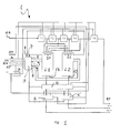
- a programmable device for storing digital video lines 2.
- the device 1 is particularly useful in TV sets with digital scan of the video frame.
- Such digital sets receive on their input a composite synchronization video signal from a receiving aerial, and perform an analog-to-digital conversion of that signal by means of a converter.
- the device 1 of this invention receives on its input a signal S1 encoded in digital form and corresponding with the line synchronization video signal received by the TV set.
- the signal S1 is encoded as sequences of so-called bytes, i.e. groups of eight bits, each corresponding with a video sample of the frame, commonly termed pixel.
- each line 2 of the video frame is encoded as a sequence of n pixels.
- the video frame consists of plural overlapping lines 2, of which the current one will be referred to as the nth line hereinafter.
- the device 1 comprises a bank of cascade interconnected registers. Specifically, five 8-bit registers T1, T2, T3, T4 and T5 are provided, the first T1 of which receives on its input said digital signal S1.
- Each of said registers is adapted to store one pixel of the video line 2, and accordingly, the series of the first four registers T1, T2, T3 and T4 will provide simultaneous access to four pixels, thereby effecting a so-called paralleling of samples of the input signal.
- the last register T5 is adapted to store an additional pixel in order to accommodate the delay introduced by the frame line scanning and produce on an output RT, additionally to the pixel of the current nth line, also the pixels of (n - 1)th and (n - 2)th lines directly preceding it.
- the operating frequency of the device 1 is scanned by a clock pulse CK.
- This pulse CK is applied to a frequency divider CKD effective to set the operating frequency of the various subsystems of the device in a manner that depends on the value of MT.
- Each of the registers T1 and T5 is connected to an output of said divider CKD and will operate, therefore, at a frequency tied to the operating mode. Said clock frequency will be one half the frequencies in the third operational instance of speed-up.
- Such registers will also receive a reset signal RT which is further applied to a control circuit 3 and the frequency divider CKD.
- L1 and L2 are respective banks of RAM memories (Random Access Memories).
- Each memory bank L1, L2 can store one line 2 of the video frame.
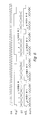
- each memory is a size of three hundred twenty cells 10 having a word length of thirty two bits each. Said cells 10 are diagramatically shown in Figure 7 at 1A...320A and 1B...320B, respectively, for each memory L1 and L2.
- Said memories have respective data inputs 11, 12 connected to each output of the first four registers T1, T2, T3 and T4.
- said memories have data outputs U1, U2 connected to corresponding inputs of a two-input multiplexer 4 having two outputs OUT1 and OUT2.
- each of the multiplexer 4 outputs are corresponding sequencer blocks 5 and 6, as required to sequence the pixels issuing in paralleled form from the memories L1 and L2.
- said blocks 5 and 6 will receive on their inputs thirty two-bit codes and produce, on their outputs OUT1 and OUT2 sequences of eight- bit words.
- the multiplexer 4 and the blocks 5 and 6 are input the reset signal RT.
- control circuit 3 will control the whole device 1, driving the other device components through its outputs.
- this circuit 3 receives on its input a signal MT containing digital information as to the type of operation that the user wants for the device 1.
- This signal MT is also input to the multiplexer 4 and the blocks 5 and 6.
- a second signal MW indicates the end of the write line; this signal is at a logic low as the electronic pencil which line scans the video frame is in its return period.
- a third signal RR indicates the end of the read line.
- circuit 3 has respective series of outputs 7, 8 and 9 connected to drive each of the memories L1 and L2 to enable the data readout/write in and address count.
- Another output SL is connected to the multiplexer 4 and the blocks 5 and 6 to ensure operational synchronization of the whole device.
- FIFO First-in-first-out
- the device 1 allows simultaneous access of the TV set to the pixels of the current line, the nth line, and to those of the two lines directly preceding it.
- references A1, A2 ...An denote the pixels of the nth line
- B1, B2 ...Bn and C1, C2 ...Cn respectively denote the values of the pixels of the (n - 1)th and (n - 2)th lines.
- T denotes the scan period of one video line 2
- t the scan period of one video line 2
- the outputs OUT1 and OUT2 of the device 1 reproduce the samples that were input at the times t - T and t - 2T.
- each memory having a single video line capacity at the generic time t, there will be in the cell 1A the first four pixels B1, B2, B3, B4 of the line preceding the current line, whereas in the cell 1B there will be the first four pixels C1, C2, C3, C4 of the line ahead of the preceding one, i.e. the (n - 2)th line.
- the input signal S1 will instead contain the code A1, A2 ... of the pixels of the current nth line.
- the device 1 Under such operating condition of the FIFO type, the device 1 will read out and output the contents of the cells 1 a and 1 B, whilst on the next clock time, it will write the new input value A1, A2, A3, A4 in the cell 1 B.
- this first operating mode allows a total of three lines to be handled, as required to process the frame in the so-called vertical domain.
- the device 1 proceeds in successive steps to read out the contents of the cells 2A and 2B and write the new value of the second group of four pixels, A5, A6, A7, A8, in the cell 2B, and so forth to the last pixel group.
- the operation Upon a line being scanned to its end, the operation will start again with reading out the cells 1A and 1 B which now contain the sequences B1, B2, B3, B4 and A1, A2, A3, A4, respectively.
- the cell 1A contains the values of the oldest line, and accordingly, the new value X1, X2, X3, X4 of the current (n + 1)th line will be written in said cell 1 A.
- the output RT of the register T5 moreover, provides simultaneously the pixels of the current line as well, which advantageously affords the possibility of accommodating the delays brought about by the RAM and multiplexer 4 updating.
- the device 1 can operate in a second mode of the LIFO (Last-in-first-out) type.
- LIFO Last-in-first-out
- This second operating mode may apply, so far still at an experimental stage, to novel methods of scanning the video frame.
- the first four pixels of the current nth line are written in the cell 1A, and simultaneously therewith, the cell B is read out which contains the first four pixels B1, B2, B3, B4 of the preceding line.
- the second group of four pixels A5, A6, A7, A8 of the current line is written in the cell 2A, while reading out the cell 2B, and so forth with each group of four line pixels.
- the first four pixels X1, X2, X3, X4 will be written in the cell 1 B, and simultaneously therewith, the last cell 320A in the memory L1 is read out.
- the next second group of four pixels X5, X6, X7, X8 will be written in the cell 2B while the last-but-one cell 319A is read in the memory L1.
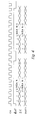
- FIG. 5 shows the patterns of the main signals involved in this mode of operation.
- the device 1 is enabled to operate in another two modes, of which the first is termed the "speed-up" mode.
- This, the third, operation mode consists of writing in a memory the current nth line and reading out the preceding, (n - 1)th line from the other memory.
- the readout is carried out here at twice the frequency of the write step; in this way, while writing in one of the two memories, the other memory can be read twice.
- a further operation mode commonly referred to as the "speed-down” mode, is similar to, but the opposite from the former case.
- the readout operation is performed at a frequency which is one half the write one. This means that only a half video line will be read at all times, thereby said half line is extended to substantially occupy the entire video line.
- the two last-named speed-up and speed-down functions find their application, within new generation digital TV sets, to the implementation of the so-called special effects (picture within the picture and magnification).
- the greatest advantage afforded by the inventive device resides in its paralleling the series of pixels input to the memories, thereby achieving in essence a relaxation of the access times to the memories.
- This device can store no less than two digitalized video lines, in conformity with current TV standards, while it can handle data relating to four different modes of operation to be selected by the user according to necessity.
- Another major advantage of the invention is that said four different functions are provided by means of a single integrated electronic component.
Landscapes
- Engineering & Computer Science (AREA)
- Multimedia (AREA)
- Signal Processing (AREA)
- Compression Or Coding Systems Of Tv Signals (AREA)
- Transforming Electric Information Into Light Information (AREA)
- Television Systems (AREA)
Priority Applications (4)
| Application Number | Priority Date | Filing Date | Title |
|---|---|---|---|
| EP90830334A EP0467004A1 (de) | 1990-07-17 | 1990-07-17 | Programmierbare Vorrichtung zur Speicherung von digitalen Videozeilen |
| US07/725,016 US5216506A (en) | 1990-07-17 | 1991-07-03 | Programmable device for storing digital video lines |
| JP3177028A JPH05161094A (ja) | 1990-07-17 | 1991-07-17 | デジタルビデオラインを記憶するためのプログラマブル装置 |
| US08/425,518 USRE36026E (en) | 1990-07-17 | 1995-04-20 | Programmable device for storing digital video lines |
Applications Claiming Priority (1)
| Application Number | Priority Date | Filing Date | Title |
|---|---|---|---|
| EP90830334A EP0467004A1 (de) | 1990-07-17 | 1990-07-17 | Programmierbare Vorrichtung zur Speicherung von digitalen Videozeilen |
Publications (1)
| Publication Number | Publication Date |
|---|---|
| EP0467004A1 true EP0467004A1 (de) | 1992-01-22 |
Family
ID=8206017
Family Applications (1)
| Application Number | Title | Priority Date | Filing Date |
|---|---|---|---|
| EP90830334A Withdrawn EP0467004A1 (de) | 1990-07-17 | 1990-07-17 | Programmierbare Vorrichtung zur Speicherung von digitalen Videozeilen |
Country Status (3)
| Country | Link |
|---|---|
| US (2) | US5216506A (de) |
| EP (1) | EP0467004A1 (de) |
| JP (1) | JPH05161094A (de) |
Families Citing this family (3)
| Publication number | Priority date | Publication date | Assignee | Title |
|---|---|---|---|---|
| US5671020A (en) * | 1995-10-12 | 1997-09-23 | Lsi Logic Corporation | Method and apparatus for improved video filter processing using efficient pixel register and data organization |
| US8059893B2 (en) * | 2007-07-25 | 2011-11-15 | The United States Of America As Represented By The Secretary Of The Navy | Method for single pass blob image analysis |
| US8155450B2 (en) * | 2007-07-25 | 2012-04-10 | The United States Of America As Represented By The Secretary Of The Navy | Apparatus for single pass blob image analysis |
Citations (3)
| Publication number | Priority date | Publication date | Assignee | Title |
|---|---|---|---|---|
| EP0246767A2 (de) * | 1986-04-28 | 1987-11-25 | Sony Corporation | Halbleiterspeicher |
| US4905096A (en) * | 1987-08-28 | 1990-02-27 | Minolta Camera Kabushiki Kaisha | Image reading arrangement |
| EP0377443A2 (de) * | 1989-01-03 | 1990-07-11 | Gte Laboratories Incorporated | Vollbildspeicher für ein FBAS-Videosignal |
Family Cites Families (1)
| Publication number | Priority date | Publication date | Assignee | Title |
|---|---|---|---|---|
| US4500908A (en) * | 1982-06-18 | 1985-02-19 | Research And Development Institute For Infosystems, Inc. | Method and apparatus for standardizing nonstandard video signals |
-
1990
- 1990-07-17 EP EP90830334A patent/EP0467004A1/de not_active Withdrawn
-
1991
- 1991-07-03 US US07/725,016 patent/US5216506A/en not_active Ceased
- 1991-07-17 JP JP3177028A patent/JPH05161094A/ja active Pending
-
1995
- 1995-04-20 US US08/425,518 patent/USRE36026E/en not_active Expired - Lifetime
Patent Citations (3)
| Publication number | Priority date | Publication date | Assignee | Title |
|---|---|---|---|---|
| EP0246767A2 (de) * | 1986-04-28 | 1987-11-25 | Sony Corporation | Halbleiterspeicher |
| US4905096A (en) * | 1987-08-28 | 1990-02-27 | Minolta Camera Kabushiki Kaisha | Image reading arrangement |
| EP0377443A2 (de) * | 1989-01-03 | 1990-07-11 | Gte Laboratories Incorporated | Vollbildspeicher für ein FBAS-Videosignal |
Non-Patent Citations (2)
| Title |
|---|
| FUNKSCHAU. vol. 60, no. 9, 08 April 1988, MUNCHEN DE pages 56 - 58; H. MITSCHKE: "BILDER AUS DEM SPEICHER" * |
| PROCEEDINGS OF THE IEEE 1988 CUSTOM INTEGRATED CIRCUITS CONFERENCE 16 May 1988, ROCHESTER pages 1 - 4; MURAKAMI ET EL.: "A 185K X 6 FIELD MEMORY FOR TV/VTR PICTURES" * |
Also Published As
| Publication number | Publication date |
|---|---|
| USRE36026E (en) | 1999-01-05 |
| JPH05161094A (ja) | 1993-06-25 |
| US5216506A (en) | 1993-06-01 |
Similar Documents
| Publication | Publication Date | Title |
|---|---|---|
| US4636783A (en) | Device for giving a pattern a rotation of an integral multiple of 90° with the pattern read from a memory on a block by block basis | |
| US5136662A (en) | Image processor for sequential processing of successive regions of an image | |
| GB2095067A (en) | Digital filter arrangement | |
| US4503469A (en) | Picture image enlarging/reducing system | |
| GB2232797A (en) | Ram based serial memory with pipelined look-ahead reading | |
| US5508967A (en) | Line memory | |
| US5627795A (en) | Timing generating device | |
| US5216506A (en) | Programmable device for storing digital video lines | |
| US5022090A (en) | Digital image processing apparatus for correctly addressing image memory | |
| GB2086200A (en) | Colour information display apparatus | |
| GB2240907A (en) | Digital signal time difference correcting circuit | |
| US4037203A (en) | High speed digital information storage system | |
| JP3108008B2 (ja) | フラッシュメモリを用いる動映像信号実時間処理方法及びその装置 | |
| EP0423007B1 (de) | Anordnung zur Erzeugung von Mosaikeffekten | |
| JP3726971B2 (ja) | 並列プロセツサ装置 | |
| JPH03206769A (ja) | 線走査をストライプによる垂直鋸歯状波走査に変換する装置 | |
| EP0632458A2 (de) | Speicherschaltung für parallelen Datenausgang | |
| SU1589288A1 (ru) | Устройство дл выполнени логических операций | |
| KR960010493B1 (ko) | 압축데이터 복원회로 | |
| JPH0145793B2 (de) | ||
| JP3311555B2 (ja) | イメージメモリ読み出し回路 | |
| SU1531160A1 (ru) | Запоминающее устройство | |
| JP2532092B2 (ja) | 状態保持回路走査方式 | |
| SU1387006A1 (ru) | Коммутационное устройство | |
| JP2508861B2 (ja) | ワ―ド多重時間スイッチ |
Legal Events
| Date | Code | Title | Description |
|---|---|---|---|
| PUAI | Public reference made under article 153(3) epc to a published international application that has entered the european phase |
Free format text: ORIGINAL CODE: 0009012 |
|
| AK | Designated contracting states |
Kind code of ref document: A1 Designated state(s): DE FR GB IT NL SE |
|
| 17P | Request for examination filed |
Effective date: 19911115 |
|
| 17Q | First examination report despatched |
Effective date: 19950217 |
|
| STAA | Information on the status of an ep patent application or granted ep patent |
Free format text: STATUS: THE APPLICATION IS DEEMED TO BE WITHDRAWN |
|
| 18D | Application deemed to be withdrawn |
Effective date: 19960322 |