EP0467005A1 - Appareil de développement électrophotographique - Google Patents
Appareil de développement électrophotographique Download PDFInfo
- Publication number
- EP0467005A1 EP0467005A1 EP90830342A EP90830342A EP0467005A1 EP 0467005 A1 EP0467005 A1 EP 0467005A1 EP 90830342 A EP90830342 A EP 90830342A EP 90830342 A EP90830342 A EP 90830342A EP 0467005 A1 EP0467005 A1 EP 0467005A1
- Authority
- EP
- European Patent Office
- Prior art keywords
- opc
- developing
- zone
- latent image
- transfer station
- Prior art date
- Legal status (The legal status is an assumption and is not a legal conclusion. Google has not performed a legal analysis and makes no representation as to the accuracy of the status listed.)
- Granted
Links
Images


Classifications
-
- G—PHYSICS
- G03—PHOTOGRAPHY; CINEMATOGRAPHY; ANALOGOUS TECHNIQUES USING WAVES OTHER THAN OPTICAL WAVES; ELECTROGRAPHY; HOLOGRAPHY
- G03G—ELECTROGRAPHY; ELECTROPHOTOGRAPHY; MAGNETOGRAPHY
- G03G15/00—Apparatus for electrographic processes using a charge pattern
- G03G15/06—Apparatus for electrographic processes using a charge pattern for developing
-
- G—PHYSICS
- G03—PHOTOGRAPHY; CINEMATOGRAPHY; ANALOGOUS TECHNIQUES USING WAVES OTHER THAN OPTICAL WAVES; ELECTROGRAPHY; HOLOGRAPHY
- G03G—ELECTROGRAPHY; ELECTROPHOTOGRAPHY; MAGNETOGRAPHY
- G03G15/00—Apparatus for electrographic processes using a charge pattern
- G03G15/06—Apparatus for electrographic processes using a charge pattern for developing
- G03G15/08—Apparatus for electrographic processes using a charge pattern for developing using a solid developer, e.g. powder developer
- G03G15/095—Removing excess solid developer, e.g. fog preventing
-
- G—PHYSICS
- G03—PHOTOGRAPHY; CINEMATOGRAPHY; ANALOGOUS TECHNIQUES USING WAVES OTHER THAN OPTICAL WAVES; ELECTROGRAPHY; HOLOGRAPHY
- G03G—ELECTROGRAPHY; ELECTROPHOTOGRAPHY; MAGNETOGRAPHY
- G03G15/00—Apparatus for electrographic processes using a charge pattern
- G03G15/14—Apparatus for electrographic processes using a charge pattern for transferring a pattern to a second base
- G03G15/16—Apparatus for electrographic processes using a charge pattern for transferring a pattern to a second base of a toner pattern, e.g. a powder pattern, e.g. magnetic transfer
- G03G15/169—Apparatus for electrographic processes using a charge pattern for transferring a pattern to a second base of a toner pattern, e.g. a powder pattern, e.g. magnetic transfer with means for preconditioning the toner image before the transfer
Definitions
- the present invention relates to a developing apparatus for use in electrophotographic copying machines and electrophotographic printers.
- an electrostatic latent image holder generally consisting in a conductive cylinder coated with a layer of photoconductive material, is juxtaposed, along a generatrix of the cylinder, to a developing material carrier, it too generally shaped as a cylinder.
- the two cylinders may be in contact os spaced apart with a predetermined gap therebetween, generally in the order of 50 to 500um.
- the two cilynders rotate in the opposite direction generally with the same peripheral speed.
- a thin layer of powder developing material known as "toner”, suitably electrized by triboelectric effect, is formed on the surface of the developing material carrier, hereinafter designated as developing roller.
- the toner which generically has magnetic properties, adheres to the developing roller, due to magnetic fields, suitably generated on the developing roller surface and due to Van Der Waals forces which acts between the toner granules and the developing roller, in spite of an electrical potential applied to the developing roller and relative to ground, of the same polarity of the electrical charge acquired by the toner, due to the triboelectric effect.
- This charge is generally negative.
- the conductive cylinder of the latent image carrier which in the following will be shortly designated as OPC, due to the extensive use of Organic Photo Conductive materials for its implementation, is generally grounded.
- An electrical charge is formed on the OPC surface by means of an electrostatic charge generator.
- This electrical charge lowers the surface potential to a predetermined value, for example -680V as to ground.
- the several OPC generatrixes so exposed then reach the developing station where the toner particles, negatively charged and immersed in the electrical field formed by the differing potential of the developing roller and the OPC, are attracted on the OPC in the OPC zones where it has been discharged at OV.
- the OPC carries the toner particles, selectively located on its surface, in a transfer zone or transfer station, where the OPC contacts, along one of its generatrixes, a printing support (generally a paper sheet) which is fed with the same speed of the OPC.
- a printing support generally a paper sheet
- the printing support is interposed between OPC and an electrostatic charge generator which charges the printing support with a positive charge.
- the positive polarization is sufficing to attract the toner from the OPC to the printing support where the toner adheres and is subsequently fixed in permanent way in a fixing station.
- the toner transfer from the developing roller to the OPC occurs not only in the zones where it is required, but at some extent also in the zones where it is not desired, with a "background" effect which hampers the quality of the images which can be obtained.
- the pulsing electrical field should cause a vibration of the toner particles which make easier their detaching from the developing roller even if the particles are weakly charged.
- the pulsing field (at the extreme an alternate field) should cause a particles rebound from the OPC to the developing roller with the consequence of a collision among particles and detaching of a greater toner amount from the developing roller.
- the present invention overcomes these limitations and provides a developing apparatus where the background effect is minimized and the image resolution is enhanced at an extreme level.
- this arrangement changes the distribution of the electrical field around the whole OPC cylinder, subjecting the toner particles lay down thereon to pulsed forces of attractive and repulsive nature which in the unexposed have an intensity sufficing to enable the migration of the charged particles from the unexposed zones to the exposed ones.
- This migration is caused by the attractive component of the electrical field, tangent to the OPC surface, due to the differing status of electrical surface bias.
- a further advantage occurs in the transfer zone where the electrical field locally reaches a high strength and where the printing support, positively biased, is subjected to a pulsing force which causes its vibration.
- the vibration, percievable as noise, must produce some triboelectric effect which electrizes uncharged particles too and some mechanical effect of capture, in addition to the electrical one, so that all the toner particles which are present on the exposed OPC zones are transferred on the printing support.
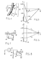
- Figure 1 shows in qualitative way the electrical field generated by a developing roller 1, biased by an alternate voltage (produced by generator 2) applied between developing roller 1 and ground, when the conductive cylinder 3 of the OPC 4 is grounded.
- the remainder of the OPC surface is immersed in an electrical field directed tangentially to the OPC surface (zone 5,6) or null (zone 7) owing to the shielding effect of the OPC itself.
- Figure 2 shows in qualitative way the electrical field generated by the conductive cylinder 3 of the OPC 4, when biased by an alternate voltage (produced by generator 2) applied between cylinder 3 and ground, when the developing roller 1 is grounded.
- the remainder of the OPC surface is immersed in an electrical field which is much lesser strong but still radial, relative to the OPC axis.
- Figure 3 shows in schematics a preferred embodiment for the apparatus of the invention.
- a developing unit 10 is juxtaposed to an OPC device 11 in form of rotating drum.
- the developing unit 10 comprises a tone reservoir 12 for toner 13 and a developing roller 14 in conductive material.
- the developing roller rotates in the direction of arrow 15, at a predetermined speed, in the order of 5 cm/sec.
- a thin toner layer 17, having a thickness imposed by a control blade 16, in the order of 50 um is drawn from reservoir 12, adheres to the surface of roller 14 and is brought towards the developing zone.
- the toner which adheres to roller 14 is negatively charged by triboelectric effect.
- the developing roller 14 is electrically biased at a negative potential in the order of -300,-500V as to ground, by a DC voltage generator 18 connected between roller 14 and ground.
- the OPC device 11 comprises a cylinder 19, in conductive material, coated with a layer 20 of photoconductive material and rotates in the direction of arrow 21.
- the OPC surface is spaced apart form the roller 14 surface by a gap having the same order of magnitude of the toner layer 17 thickness or slightly greater.
- the electrical potential of the surface charge is controlled by a DC voltage generator 24, which applies a voltage in the order of -700V between the grid shield 23 and the conductive cylinder 19 of the OPC device.
- the so charged OPC surface is selectively exposed to an electromagnetic radiation 25, controlled by an image generator 26, at an exposure station located downstream of the corotron and upstream of the developing station.
- the photoconductive material allows the electrical charges at the surface to discharge on the conductive cylinder 19.
- the OPC surfaces takes a substantially nul potential as to the potential of cylinder 19.
- the cylinder 19 is electrically biased by a generator 27 of AC voltage in the order of 200-500V peak; connected between cylinder 19 and ground.
- the frequency of the AC voltage may be selected within very broad limits, with a lower limit which essentially depends on the developing speed, say the peripheral speed of the OPC.
- the upper limit seems related to the size and the mass of the toner particles in inverse relation.
- Figure 4 shows a portion 30 of the OPC which comprises an unexposed zone 31, hence with a negative surface charge (of -700V relative to the conductive cylinder 19), and an exposed zone 32 which has been discharged and on which toner particles lay down.
- a negative surface charge of -700V relative to the conductive cylinder 19
- an exposed zone 32 which has been discharged and on which toner particles lay down.
- the negative charge of the toner particles does not change in substantive way the electrical fields generated by the external biasing and by the OPC polarization.
- An AC bias of 400V applied to the conductive cylinder 19 generates a radial field shown by arrows 33,34.
- the radial field is overlapped with the field generated by the OPC polarization charges (-700V) so that the potential of the space surrounding zone 31 may be represented in its extreme conditions by diagrams A,B of figure 5.
- the potential of the space surrounding zone 32 is represented in its extreme conditions by diagrams C,D of Fig. 6.
- a generic toner particle P (Fig.4), negatively charged and located at the surface of zone 31, is therefore subjected to a repulsive force of variable amplitude which tends to push it away from the surface, opposing to the non electrostatic forces (Van Der Waals forces) which retain it at the surface.
- This repulsive force provides a relative mobility to the particle.
- zone 31,32 a tangential electrical field due to the presence of electrical charge in zone 31 and to the missing of electrical charges in zone 32 overlaps with the radial field generated by voltage generator 27 and by the charges in zone 31.
- This tangential force tends to pull particle P towards zone 32.
- particle P When particle P is immersed in an electrical field, it is subjected to dielectric polarization, hence to a radial pulsing force.
- the development apparatus of the invention enables to obtain highly contrasted images having highly defined edges and a substantive background reduction.
- the transfer station comprises a corotron 40 facing the OPC drum 11.
- the corotron comprises a ionizing wire 41, electrically biased at an high positive potential in the order of + 3 + 5 KV by a voltage generator 42 and a grid shield 43 ground connected.
- a printing support 44 is brought in contact with the OPC at the transfer station and is fed, interposed between corotron 40 and OPC11, at a speed equal to the peripheral OPC speed.
- Corotron 40 diffuses positive electrical charges on the printing support, which is electrized, thus generating a strong electrical field between printing support and OPC.
- This field detaches the toner particles (negatively charged) from the OPC and attract them onto the printing support for subsequent fixing in a fixing station.
- the phenomenom is exalted, in the exposed zones, by the presence of contiguous particles, mostly charged, hence subjected to attractive and repulsive forces with consequent relative displacement among charged particles and neutral ones and related friction.
- shield 43 is provided with a conductive guiding blade 45 juxstaposed to the OPC surface at a distance in the order of 2-3 mm from OPC at the printing support input and at a distance in the order of 0,5 mm at the output.
- the electrical field generated by the alternate biasing of the OPC is particularly strong, at a level such that owing to such field the printing support, ionized by charge migration from the zone facing the corotron grid to the zone interposed between OPC and guiding blade, vibrates causing a noise at the frequency of the alternate biasing.
- the electrical field is so strong that the triboelectric effect and the particle migration are increased.
- the printing support itself exert a mechanical action of variable compression on the toner facilitating the transfer.
- the only drawback is noise generation, which may be completely avoided by electrically connecting shield 43 to the conductive cylinder 19, as shown in figure 7, or limited to an acceptable level by biasing shield 43 with a fraction of the biasing potential of cilinder 19.
- VDR voltage dependent resistor
- zener diode connected between cylinder 19 and shield 43 may be a substitute for such voltage divider.
- the same arrangements may be used to generate the several biasing voltages required in the apparatus, departing from the voltage generated by one or two voltage generators only (respectively a positive and a negative voltage generator).
- a latent image carrier OPC
- a toner carrier both in form of rotating cylinders
- the invention is equally applicable in case one or both of these elements are in form other than a rotating cylinder, such as a movable belt mounted on rotating drums.
- the essential aspect of the invention consists in the generation of a variable electrical field perpendicular to the surface of the latent image carrier, which field acts on a relatively wide area of the carrier comprised between the development station and the transfer station.
- the electrical alternate biasing of cylinder 19 of the OPC is only a preferred embodiment, because it assures the generation of such variable field extending to the whole OPC surface and including the development station and the fixing station.
- This strengthening of the electrical alternate field generated by the OPC may be obtained by juxtaposing to the OPC surface a conductive armature 48 located between the development station and the transfer station and electrically grounded as shown in Fig.3.
- Such armature is preferably located at a distance from the OPC surface comprised between 1 mm and 5 mm and extends along the OPC surface for an arc having a length comprised between 2 and 20 mm or more depending on the peripheral distance between the developing station and the transfer station.
Landscapes
- Physics & Mathematics (AREA)
- General Physics & Mathematics (AREA)
- Developing For Electrophotography (AREA)
- Dry Development In Electrophotography (AREA)
- Electrostatic Charge, Transfer And Separation In Electrography (AREA)
Priority Applications (5)
| Application Number | Priority Date | Filing Date | Title |
|---|---|---|---|
| EP90830342A EP0467005B1 (fr) | 1990-07-20 | 1990-07-20 | Appareil de développement électrophotographique |
| DE69006024T DE69006024T2 (de) | 1990-07-20 | 1990-07-20 | Elektrophotographisches Entwicklungsgerät. |
| US07/731,690 US5250995A (en) | 1990-07-20 | 1991-07-17 | Electrophotographic developing apparatus having image quality improving devices |
| JP3179839A JPH05142934A (ja) | 1990-07-20 | 1991-07-19 | 電子写真用現像装置 |
| KR1019910012526A KR920003117A (ko) | 1990-07-20 | 1991-07-20 | 전자 사진현상장치 |
Applications Claiming Priority (1)
| Application Number | Priority Date | Filing Date | Title |
|---|---|---|---|
| EP90830342A EP0467005B1 (fr) | 1990-07-20 | 1990-07-20 | Appareil de développement électrophotographique |
Publications (2)
| Publication Number | Publication Date |
|---|---|
| EP0467005A1 true EP0467005A1 (fr) | 1992-01-22 |
| EP0467005B1 EP0467005B1 (fr) | 1994-01-12 |
Family
ID=8206018
Family Applications (1)
| Application Number | Title | Priority Date | Filing Date |
|---|---|---|---|
| EP90830342A Expired - Lifetime EP0467005B1 (fr) | 1990-07-20 | 1990-07-20 | Appareil de développement électrophotographique |
Country Status (5)
| Country | Link |
|---|---|
| US (1) | US5250995A (fr) |
| EP (1) | EP0467005B1 (fr) |
| JP (1) | JPH05142934A (fr) |
| KR (1) | KR920003117A (fr) |
| DE (1) | DE69006024T2 (fr) |
Families Citing this family (2)
| Publication number | Priority date | Publication date | Assignee | Title |
|---|---|---|---|---|
| US6684047B2 (en) * | 2000-04-10 | 2004-01-27 | Seiko Epson Corporation | Image forming apparatus with reduced image defects |
| US20120069113A1 (en) * | 2010-09-17 | 2012-03-22 | Toshiba Tec Kabushiki Kaisha | Image forming apparatus, medium processing apparatus, and image forming method |
Citations (3)
| Publication number | Priority date | Publication date | Assignee | Title |
|---|---|---|---|---|
| US4491408A (en) * | 1984-01-03 | 1985-01-01 | Xerox Corporation | Electrostatographic system development modulation |
| US4647186A (en) * | 1985-11-04 | 1987-03-03 | Eastman Kodak Company | Biased scavenging grid for electrographic apparatus |
| US4701042A (en) * | 1984-12-03 | 1987-10-20 | Olympus Optical Co., Ltd. | Duplicating apparatus |
Family Cites Families (7)
| Publication number | Priority date | Publication date | Assignee | Title |
|---|---|---|---|---|
| US4039257A (en) * | 1974-07-25 | 1977-08-02 | Xerox Corporation | Pretransfer corotron switching |
| JPS55147651A (en) * | 1979-05-07 | 1980-11-17 | Ricoh Co Ltd | Electrophotographic apparatus |
| JPS5650340A (en) * | 1979-09-29 | 1981-05-07 | Canon Inc | Electrophotographic apparatus |
| JPS5931982A (ja) * | 1982-08-16 | 1984-02-21 | Oki Electric Ind Co Ltd | 磁性トナ−転写装置 |
| JPS6095471A (ja) * | 1983-10-28 | 1985-05-28 | Ricoh Co Ltd | 転写装置 |
| JPS60241068A (ja) * | 1984-05-16 | 1985-11-29 | Oki Electric Ind Co Ltd | 電子写真装置 |
| US4984022A (en) * | 1987-11-26 | 1991-01-08 | Minolta Camera Kabushiki Kaisha | Image forming apparatus having means for attenuating bias voltage of the developing sleeve |
-
1990
- 1990-07-20 DE DE69006024T patent/DE69006024T2/de not_active Expired - Fee Related
- 1990-07-20 EP EP90830342A patent/EP0467005B1/fr not_active Expired - Lifetime
-
1991
- 1991-07-17 US US07/731,690 patent/US5250995A/en not_active Expired - Fee Related
- 1991-07-19 JP JP3179839A patent/JPH05142934A/ja active Pending
- 1991-07-20 KR KR1019910012526A patent/KR920003117A/ko not_active Ceased
Patent Citations (3)
| Publication number | Priority date | Publication date | Assignee | Title |
|---|---|---|---|---|
| US4491408A (en) * | 1984-01-03 | 1985-01-01 | Xerox Corporation | Electrostatographic system development modulation |
| US4701042A (en) * | 1984-12-03 | 1987-10-20 | Olympus Optical Co., Ltd. | Duplicating apparatus |
| US4647186A (en) * | 1985-11-04 | 1987-03-03 | Eastman Kodak Company | Biased scavenging grid for electrographic apparatus |
Non-Patent Citations (3)
| Title |
|---|
| PATENT ABSTRACTS OF JAPAN, vol. 10, no. 250 (P-491)[2306], 28th August 1986; & JP-A-61 77 869 (MITA IND. CO., LTD) 21-04-1986 * |
| PATENT ABSTRACTS OF JAPAN, vol. 7, no. 75 (P-187)[1220], 29th March 1983; & JP-A-58 5755 (CANON K.K.) 13-01-1983 * |
| PATENT ABSTRACTS OF JAPAN, vol. 8, no. 60 (P-262)[1497], 22nd March 1984; & JP-A-58 208 779 (RICOH K.K.) 05-12-1983 * |
Also Published As
| Publication number | Publication date |
|---|---|
| EP0467005B1 (fr) | 1994-01-12 |
| US5250995A (en) | 1993-10-05 |
| DE69006024D1 (de) | 1994-02-24 |
| DE69006024T2 (de) | 1994-05-26 |
| KR920003117A (ko) | 1992-02-29 |
| JPH05142934A (ja) | 1993-06-11 |
Similar Documents
| Publication | Publication Date | Title |
|---|---|---|
| US3866574A (en) | Xerographic developing apparatus | |
| US4868600A (en) | Scavengeless development apparatus for use in highlight color imaging | |
| US4876575A (en) | Printing apparatus including apparatus and method for charging and metering toner particles | |
| US3890929A (en) | Xerographic developing apparatus | |
| US5144371A (en) | Dual AC/dual frequency scavengeless development | |
| JPS60158582A (ja) | コロナ帯電装置 | |
| US4579441A (en) | Detacking apparatus | |
| EP0533347A2 (fr) | Système de développement | |
| US4990958A (en) | Reload member for a single component development housing | |
| US3464818A (en) | Method of photoelectric copying | |
| JPH0473795B2 (fr) | ||
| US5276484A (en) | Piezo-active photoreceptors and system application | |
| EP0467005B1 (fr) | Appareil de développement électrophotographique | |
| EP0147187A1 (fr) | Dispositif de nettoyage pour surface retenant une charge électrique | |
| US3932877A (en) | Electrophotographic recording system with plate cleaning | |
| JPH06105379B2 (ja) | 残留トナー除去装置 | |
| US4694310A (en) | Method and apparatus of electrophotography | |
| US3870515A (en) | Method for electrostatic paper stripping by neutralization of transfer charge | |
| EP1359473B1 (fr) | Système électrodynamique de transfert de révélateur | |
| US3851962A (en) | Electrostatic hold down apparatus | |
| JPH10207222A (ja) | 静電潜像の現像機構 | |
| US5381214A (en) | Electrophotographic charging device | |
| JPH1020618A (ja) | 転写前画像修正可能な静電画像処理装置 | |
| EP0138376B1 (fr) | Procédé et appareil d'électrophotographie | |
| US4103994A (en) | Recording plate |
Legal Events
| Date | Code | Title | Description |
|---|---|---|---|
| PUAI | Public reference made under article 153(3) epc to a published international application that has entered the european phase |
Free format text: ORIGINAL CODE: 0009012 |
|
| AK | Designated contracting states |
Kind code of ref document: A1 Designated state(s): DE FR GB IT |
|
| 17P | Request for examination filed |
Effective date: 19920402 |
|
| 17Q | First examination report despatched |
Effective date: 19930430 |
|
| GRAA | (expected) grant |
Free format text: ORIGINAL CODE: 0009210 |
|
| AK | Designated contracting states |
Kind code of ref document: B1 Designated state(s): DE FR GB IT |
|
| ITF | It: translation for a ep patent filed | ||
| REF | Corresponds to: |
Ref document number: 69006024 Country of ref document: DE Date of ref document: 19940224 |
|
| ET | Fr: translation filed | ||
| PLBE | No opposition filed within time limit |
Free format text: ORIGINAL CODE: 0009261 |
|
| STAA | Information on the status of an ep patent application or granted ep patent |
Free format text: STATUS: NO OPPOSITION FILED WITHIN TIME LIMIT |
|
| 26N | No opposition filed | ||
| PGFP | Annual fee paid to national office [announced via postgrant information from national office to epo] |
Ref country code: GB Payment date: 19970620 Year of fee payment: 8 |
|
| PGFP | Annual fee paid to national office [announced via postgrant information from national office to epo] |
Ref country code: DE Payment date: 19970623 Year of fee payment: 8 |
|
| PGFP | Annual fee paid to national office [announced via postgrant information from national office to epo] |
Ref country code: FR Payment date: 19970731 Year of fee payment: 8 |
|
| PG25 | Lapsed in a contracting state [announced via postgrant information from national office to epo] |
Ref country code: GB Free format text: LAPSE BECAUSE OF NON-PAYMENT OF DUE FEES Effective date: 19980720 |
|
| GBPC | Gb: european patent ceased through non-payment of renewal fee |
Effective date: 19980720 |
|
| PG25 | Lapsed in a contracting state [announced via postgrant information from national office to epo] |
Ref country code: FR Free format text: LAPSE BECAUSE OF NON-PAYMENT OF DUE FEES Effective date: 19990331 |
|
| PG25 | Lapsed in a contracting state [announced via postgrant information from national office to epo] |
Ref country code: DE Free format text: LAPSE BECAUSE OF NON-PAYMENT OF DUE FEES Effective date: 19990501 |
|
| REG | Reference to a national code |
Ref country code: FR Ref legal event code: ST |
|
| PG25 | Lapsed in a contracting state [announced via postgrant information from national office to epo] |
Ref country code: IT Free format text: LAPSE BECAUSE OF NON-PAYMENT OF DUE FEES;WARNING: LAPSES OF ITALIAN PATENTS WITH EFFECTIVE DATE BEFORE 2007 MAY HAVE OCCURRED AT ANY TIME BEFORE 2007. THE CORRECT EFFECTIVE DATE MAY BE DIFFERENT FROM THE ONE RECORDED. Effective date: 20050720 |