EP0467736B1 - Magnetoresistiver Effekt verwendender Lesemagnetkopf - Google Patents
Magnetoresistiver Effekt verwendender Lesemagnetkopf Download PDFInfo
- Publication number
- EP0467736B1 EP0467736B1 EP91401817A EP91401817A EP0467736B1 EP 0467736 B1 EP0467736 B1 EP 0467736B1 EP 91401817 A EP91401817 A EP 91401817A EP 91401817 A EP91401817 A EP 91401817A EP 0467736 B1 EP0467736 B1 EP 0467736B1
- Authority
- EP
- European Patent Office
- Prior art keywords
- magnetic
- magnetic layer
- layer
- conductor
- layers
- Prior art date
- Legal status (The legal status is an assumption and is not a legal conclusion. Google has not performed a legal analysis and makes no representation as to the accuracy of the status listed.)
- Expired - Lifetime
Links
- 230000005291 magnetic effect Effects 0.000 title claims description 186
- 230000000694 effects Effects 0.000 title description 19
- 239000004020 conductor Substances 0.000 claims description 72
- 239000000758 substrate Substances 0.000 claims description 15
- 230000005415 magnetization Effects 0.000 claims description 6
- 239000011159 matrix material Substances 0.000 claims description 4
- 239000010410 layer Substances 0.000 description 96
- 238000004519 manufacturing process Methods 0.000 description 6
- 230000000903 blocking effect Effects 0.000 description 5
- 230000005290 antiferromagnetic effect Effects 0.000 description 4
- 230000008878 coupling Effects 0.000 description 4
- 238000010168 coupling process Methods 0.000 description 4
- 238000005859 coupling reaction Methods 0.000 description 4
- 229910045601 alloy Inorganic materials 0.000 description 3
- 239000000956 alloy Substances 0.000 description 3
- 230000005294 ferromagnetic effect Effects 0.000 description 3
- 238000000034 method Methods 0.000 description 3
- 239000002356 single layer Substances 0.000 description 3
- RYGMFSIKBFXOCR-UHFFFAOYSA-N Copper Chemical compound [Cu] RYGMFSIKBFXOCR-UHFFFAOYSA-N 0.000 description 2
- XEEYBQQBJWHFJM-UHFFFAOYSA-N Iron Chemical compound [Fe] XEEYBQQBJWHFJM-UHFFFAOYSA-N 0.000 description 2
- 230000009471 action Effects 0.000 description 2
- 230000008901 benefit Effects 0.000 description 2
- 229910052802 copper Inorganic materials 0.000 description 2
- 239000010949 copper Substances 0.000 description 2
- 238000013500 data storage Methods 0.000 description 2
- 238000010586 diagram Methods 0.000 description 2
- 238000009792 diffusion process Methods 0.000 description 2
- 230000001939 inductive effect Effects 0.000 description 2
- 239000000463 material Substances 0.000 description 2
- 238000005259 measurement Methods 0.000 description 2
- 229910000889 permalloy Inorganic materials 0.000 description 2
- 229910052710 silicon Inorganic materials 0.000 description 2
- 239000010703 silicon Substances 0.000 description 2
- 230000007704 transition Effects 0.000 description 2
- 241001080024 Telles Species 0.000 description 1
- QXZUUHYBWMWJHK-UHFFFAOYSA-N [Co].[Ni] Chemical compound [Co].[Ni] QXZUUHYBWMWJHK-UHFFFAOYSA-N 0.000 description 1
- 239000000969 carrier Substances 0.000 description 1
- 238000010276 construction Methods 0.000 description 1
- 238000005520 cutting process Methods 0.000 description 1
- 230000001419 dependent effect Effects 0.000 description 1
- 238000000151 deposition Methods 0.000 description 1
- 238000006073 displacement reaction Methods 0.000 description 1
- 238000005516 engineering process Methods 0.000 description 1
- 238000005530 etching Methods 0.000 description 1
- 239000011521 glass Substances 0.000 description 1
- 229910052742 iron Inorganic materials 0.000 description 1
- 239000000696 magnetic material Substances 0.000 description 1
- 230000004048 modification Effects 0.000 description 1
- 238000012986 modification Methods 0.000 description 1
- 230000004044 response Effects 0.000 description 1
- 229910000702 sendust Inorganic materials 0.000 description 1
- 229910052709 silver Inorganic materials 0.000 description 1
- 239000004332 silver Substances 0.000 description 1
- 230000000087 stabilizing effect Effects 0.000 description 1
- 239000010409 thin film Substances 0.000 description 1
Images

Classifications
-
- G—PHYSICS
- G11—INFORMATION STORAGE
- G11B—INFORMATION STORAGE BASED ON RELATIVE MOVEMENT BETWEEN RECORD CARRIER AND TRANSDUCER
- G11B5/00—Recording by magnetisation or demagnetisation of a record carrier; Reproducing by magnetic means; Record carriers therefor
- G11B5/127—Structure or manufacture of heads, e.g. inductive
- G11B5/33—Structure or manufacture of flux-sensitive heads, i.e. for reproduction only; Combination of such heads with means for recording or erasing only
- G11B5/39—Structure or manufacture of flux-sensitive heads, i.e. for reproduction only; Combination of such heads with means for recording or erasing only using magneto-resistive devices or effects
- G11B5/3903—Structure or manufacture of flux-sensitive heads, i.e. for reproduction only; Combination of such heads with means for recording or erasing only using magneto-resistive devices or effects using magnetic thin film layers or their effects, the films being part of integrated structures
-
- G—PHYSICS
- G11—INFORMATION STORAGE
- G11B—INFORMATION STORAGE BASED ON RELATIVE MOVEMENT BETWEEN RECORD CARRIER AND TRANSDUCER
- G11B5/00—Recording by magnetisation or demagnetisation of a record carrier; Reproducing by magnetic means; Record carriers therefor
- G11B5/127—Structure or manufacture of heads, e.g. inductive
- G11B5/33—Structure or manufacture of flux-sensitive heads, i.e. for reproduction only; Combination of such heads with means for recording or erasing only
- G11B5/332—Structure or manufacture of flux-sensitive heads, i.e. for reproduction only; Combination of such heads with means for recording or erasing only using thin films
-
- G—PHYSICS
- G11—INFORMATION STORAGE
- G11B—INFORMATION STORAGE BASED ON RELATIVE MOVEMENT BETWEEN RECORD CARRIER AND TRANSDUCER
- G11B5/00—Recording by magnetisation or demagnetisation of a record carrier; Reproducing by magnetic means; Record carriers therefor
- G11B5/127—Structure or manufacture of heads, e.g. inductive
- G11B5/33—Structure or manufacture of flux-sensitive heads, i.e. for reproduction only; Combination of such heads with means for recording or erasing only
- G11B5/39—Structure or manufacture of flux-sensitive heads, i.e. for reproduction only; Combination of such heads with means for recording or erasing only using magneto-resistive devices or effects
- G11B5/3903—Structure or manufacture of flux-sensitive heads, i.e. for reproduction only; Combination of such heads with means for recording or erasing only using magneto-resistive devices or effects using magnetic thin film layers or their effects, the films being part of integrated structures
- G11B5/3906—Details related to the use of magnetic thin film layers or to their effects
- G11B5/3945—Heads comprising more than one sensitive element
- G11B5/3948—Heads comprising more than one sensitive element the sensitive elements being active read-out elements
- G11B5/3958—Heads comprising more than one sensitive element the sensitive elements being active read-out elements the active elements being arranged in a single plane, e.g. "matrix" disposition
-
- G—PHYSICS
- G11—INFORMATION STORAGE
- G11B—INFORMATION STORAGE BASED ON RELATIVE MOVEMENT BETWEEN RECORD CARRIER AND TRANSDUCER
- G11B5/00—Recording by magnetisation or demagnetisation of a record carrier; Reproducing by magnetic means; Record carriers therefor
- G11B5/48—Disposition or mounting of heads or head supports relative to record carriers ; arrangements of heads, e.g. for scanning the record carrier to increase the relative speed
- G11B5/49—Fixed mounting or arrangements, e.g. one head per track
- G11B5/4969—Details for track selection or addressing
Definitions
- the invention relates to magnetic read heads in which a magneto-resistive effect is implemented, using magneto-resistive elements of the multilayer type.
- the speed of rotation of magnetic reading heads is high and it is combined with displacement of the magnetic strip, and in this case it is possible to extract enough signal with a purely inductive read head.
- the magnetic field coming from a track of the magnetic strip is channeled by a magnetic circuit and generates a current in a solenoid associated with the magnetic circuit.
- the rotating magnetic heads have drawbacks, in particular when it comes to the weight and size of the mechanical parts which must rotate at relatively high speed, and also as regards reliability.
- An alternative to recording solutions with rotating heads consists in recording and re-reading the tracks of the magnetic tape, using devices fixed relative to the magnetic tape: for example using a single device comprising a or several working magnetic heads; either in writing, that is to say in recording, or in reading or even using two devices, one of which is for writing and the other for reading.
- the movement of the magnetic strip is slow and if the magnetic heads are fixed relative to the strip, the variations of the magnetic field occur at relatively low speed (typically a few centimeters per second), and it is impossible under these conditions extract enough signal from a head purely inductive.
- the magnetic reading heads which use the magneto-resistive effect can be fixed in front of the magnetic strip, while delivering a sufficient useful signal.
- magneto-resistive effect sensors are used in various magnetic stripe reading devices. These sensors are placed in the zone of influence of a mobile magnetic track, and their variations in electrical resistance are detected in response to variations in the magnetic field recorded on the magnetic track of the strip.
- alloys commonly used to constitute a magneto-resistive element or sensor mention may in particular be made of ferromagnetic alloys such as for example Permalloy (Fe80Ni20).
- the magneto-resistive elements of the multilayer type are of greater complexity of construction than the monolayer type elements, but they offer the advantage of providing a larger useful signal.
- the useful signal that is to say the variation of the current which circulates in the magnetic layers, is linked to the ratio of the variation in resistance ⁇ R to the resistance R between these two layers: this ratio is around 10% in the case of magnetoresistive elements of the multilayer type, while it is only around 3% in the case of the monolayer type.
- the present invention applies to magnetic read heads incorporating magneto-resistive elements of the multilayer type. It aims in particular to simplify the production of such heads in order to facilitate their collective production, both for unitary use and for combining a large number of read heads in the same magnetic device, for example for reading in parallel a large number of magnetic tracks.
- a magnetic reading device according to the invention is defined in claim 1.
- FIG. 1 shows a magnetic reading device 1 comprising several magnetic reading heads TL1, TL2, TL3, TL4 according to the invention, produced on the same substrate 2.
- four reading heads TL1 to TL4 are shown to illustrate the fact that the structure of these read heads lends itself particularly well to a collective production of these heads on the same substrate, either to then separate them by cutting to make them individual heads, or to make a device magnetic comprising a plurality of read heads.
- the device 1 may include a smaller number of these read heads, or a much larger number.
- Each read head comprises a magneto-resistive element MR of the multilayer type.
- each magneto-resistive element MR comprises so as itself conventional two superposed magnetic layers 6,7 of which one is a stable magnetic layer and the other is a sensitive magnetic layer; these two magnetic layers 6,7 are separated by a non-magnetic layer 3.
- the first magnetic layer 6, the closest to the substrate 2 constitutes the stable magnetic layer; it has a stable magnetization direction, that is to say that its coercive field is much larger than that of the second magnetic layer 7.
- the second magnetic layer 7 constitutes a sensitive magnetic layer 7 whose direction of magnetization can tip under the influence of an external magnetic field.
- the two magnetic layers 6,7 and the non-magnetic layer 3 are produced in a conventional manner so that the two magnetic layers 6,7 have an anti-ferromagnetic coupling.
- the stable magnetic layer 6 and the sensitive magnetic layer 7 can be made of a ferromagnetic alloy such as for example Nickel-Cobalt Ni x Co y for the stable magnetic layer 6, and Permalloy Fe80 Ni20 for the sensitive magnetic layer 7; and the non-magnetic layer 3 can be silver or copper.
- the two ferro-magnetic layers 6,7 may both be made of the same material, iron for example, but with different thicknesses E1, E2, several times greater for the thickness E1 of the stable magnetic layer 6 as for the thickness E2 of the sensitive layer 7: for example E1 of the order of 1 ⁇ m and E2 of the order of 0.01 ⁇ m; the thickness of the non-magnetic layer being for example 0.001 ⁇ m.
- the sensitive layer 7 must be subjected to the influence of a magnetic field inscribed on a magnetic track 8 (for clarity of the figure, a single magnetic track 8 is shown in dotted lines). To this end, in accordance with the invention, this magnetic field is led to the magneto-resistive element MR using a magnetic circuit of the ring type, comprising a gap 10; the air gap 10 is made in the immediate vicinity of the runway runway magnetic 8.
- This arrangement offers the advantage of being able to arrange the layers 6, 7, 3, 3 of the magneto-resistive element MR in planes parallel to the plane of the substrate and to the running plane of track 8, which results in at the same time, on the one hand, the possibility of using a large number of read heads located very close to one another to simultaneously play a large number of tracks; and whence results, on the other hand, a general arrangement which favors the manufacture of these read heads by a collective production of these heads, in particular by the technology of thin layers; even if, possibly, these heads must be separated from each other after collective production, to constitute individual heads.
- the magnetic circuit comprises two magnetic poles 11,12 arranged on either side of the air gap 10 as shown in FIG. 1. These two magnetic poles 11,12 are each extended by a magnetic piece 13,14 which is in contact with the sensitive magnetic layer 7.
- the magnetic circuit is constituted by the two magnetic poles 11,12, the two magnetic parts 13,14 and the sensitive magnetic layer 7 which is inserted between this two magnetic parts 13,14.
- the two magnetic poles 11, 12 are contained in a plane very close to the running plane of track 8; the two magnetic parts 13, 14 are located in a plane further from the track 8 than the magnetic poles 11, 12; and finally, the sensitive magnetic layer 7 is located in a plane even further from the track 8.
- Such a ring structure is particularly suitable for making the power supply connections of the stable magnetic layers and of the sensitive magnetic layers 7 by conductors located in different planes.
- a first electrical conductor 20 is produced between the substrate 2 and the stable magnetic layer 6, with which this first conductor is in contact ; and on the other hand, a second electrical conductor 21 is produced between the magnetic heads 11, 12 and the sensitive magnetic layer 7 with which this second conductor is in contact.
- the second conductor 21 is produced substantially in the same plane as that of the magnetic parts 13, 14, so that it can pass through the ring of the magnetic circuit and extend in a direction substantially perpendicular to that of the first conductor 20 .
- the magnetic reading device can comprise on the one hand, a plurality of first conductors 20 constituting an array of column conductors X1, X2 and on the other hand, a plurality of second conductors 21 constituting an array of row conductors Y1, Y2 crossed with the column conductors.
- Each read head TL1 to TL4 is arranged substantially at an intersection of a column conductor X1, X2 with a row conductor Y1, Y2, and its electrical supply is carried out using the column conductor X1, X2 and the row conductor Y1 , Y2 which form the corresponding intersection.
- the designation "row” or “column” given to the conductors is arbitrary and does not prejudge their orientation, and that the columns are not necessarily perpendicular to the rows.
- the magnetic heads TL1 to TL4 are arranged in rows and columns to which correspond a row conductor Y1, Y2 and a column conductor X1, X2; each row conductor Y1, Y2 being in contact with all the sensitive magnetic layers 7 of the same row, and each column conductor X1, X2 being in contact with all the stable magnetic layers 6 of the same column.
- FIG. 1 The structure shown in FIG. 1 can be produced in different ways, all known to specialists, in particular by the thin film technique. This technique is now well known and does not require to be illustrated.
- the substrate 2 is made of a non-magnetic material, glass for example, or insulating silicon.
- a layer of a conductive material for example copper, is deposited in which the column conductors X1, X2 are produced by etching.
- These conductors can also be integrated into the substrate 2, as in the example in FIG. 1, by making in itself conventional grooves which are then filled with the conductive material.
- the whole is covered with a magnetic layer, intended to form the stable magnetic layers 6.
- a non-magnetic layer is deposited intended to form the non-magnetic layers 3.
- a magnetic layer is deposited on the whole intended to form the sensitive magnetic layers 6.
- the three layers 7, 6, 3, are etched in the form of islands each constituting a magneto-resistive element MR.
- An insulating layer 27 is then deposited to separate the islands, then a layer of a conductive material which is etched to form line conductors Y1, Y2, that is to say second conductors 21.
- the magnetic poles 11, 12 are then produced separated by the air gap, for example by successively depositing several layers of "Sendust" according to a known technique, as for example described in a French patent application 86 14974 in the name of THOMSON-CSF.
- the measurement signal corresponding to the magnetic field inscribed on the track 8 consists of a variation of a measurement current which flows between the stable magnetic layer 6 and the sensitive magnetic layer 7 when a control voltage is applied between these two layers 6,7.
- the control voltage is applied using a column conductor X1, X2 and a line conductor Y1, Y2, and the current flows perpendicular to the plane of the magnetic layers 6, 7 in and between these two conductors.
- the read head structure shown in FIG. 1 has been described with reference to a head in which a magneto-resistive effect is implemented using a MR multilayer magnetic structure, this multilayer magnetic structure being of the type comprising a stable magnetic layer 6 and a sensitive magnetic layer 7 separated by a non-magnetic layer 3.
- This action of the magnetic field inscribed on a magnetic track to be read causes a tilting of the magnetic orientation of the sensitive layer, tilting which gives rise to a variation of an electric current which circulates in the two magnetic layers.
- the non-magnetic layer is electrically conductive and allows current to flow between the two magnetic layers.
- the phenomenon implemented is in this case purely magneto-resistive.
- the non-magnetic layer 3 is an insulating or semiconducting layer, for example made of silicon with a thickness of the order of 0.01 ⁇ m; the magnetic layers 6, 7 being of the same nature as in the previous case.
- the tilting of the magnetic orientation of the sensitive layer 7 causes a modification of the amplitude of this "tunnel" current, in a similar way to the variation in amplitude of the current in the purely magneto-resistive case.
- magnetoresistive element of the multilayer type to define both a structure implementing the purely magneto-resistive effect as a structure implementing the "Tunnel effect.”
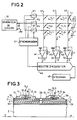
- FIG. 2 schematically shows by way of nonlimiting example, a reading device according to the invention, in which a plurality of reading heads, similar to the reading heads TL1 to TL4 shown in FIG. 1, are selected by addressing of matrix type.
- the reading device 1 shown in FIG. 2 comprises only three row conductors Y1, Y2, Y3 crossed with three column conductors X1, X2, X3, giving rise to nine intersections each comprising a reading head TL1 to TL9 ; but of course, in practice the number of conductors and rows and columns can be much greater.
- the TL1 to TL9 read heads being of the multilayer magneto-resistive type, they are represented in the form of resistors.
- one end of the resistor constituted for example by the sensitive magnetic layer 7 is connected to the line conductor Y1 to Y3 of its intersection; and the other end of the resistor, that is to say the stable magnetic layer 6, is connected to the column electrode X1 to X3 of the same intersection.
- a first read head line L1 comprises the heads TL1, TL2, TL3, the stable magnetic layers 6 of which are connected respectively to the first, second and third column conductors X1, X2 and X3; while the stable magnetic layers 7 are connected to the first line conductor Y1.
- the read heads of lines L2 and L3 are connected in a similar way to the line and column conductors of their intersection.
- the reading device 1 comprises a voltage generator 30 producing a control voltage VC (with respect to a reference potential which is ground for example); the control voltage VC is intended to be applied to the read heads TL1 to TL9 and more precisely to the magneto-resistive elements.
- a voltage generator 30 producing a control voltage VC (with respect to a reference potential which is ground for example); the control voltage VC is intended to be applied to the read heads TL1 to TL9 and more precisely to the magneto-resistive elements.
- the reading device 1 further comprises a door device comprising as many doors P1 to P3 (analog for example) as there are line conductors Y1 to Y3.
- each door P1 to P3 is connected to one of the line conductors (Y1 to Y3) and the door inputs are all connected to an output of the voltage generator 30 delivering the control voltage VC.
- Each gate P1 to P3 is controlled by a synchronization circuit 31, which decides on the "blocking" state or the "passing" state of the gate considered.
- the control voltage VC is applied to the line conductor Y1 to Y3, under a low impedance; while in the “blocking” state the line conductor is not connected to the voltage generator 30, except through a very high impedance; in other words, with the "blocking" state of a given door P1 to P3, the corresponding line conductor is in "the air", that is to say is not connected to anything.
- the column conductors X1 to X3 are brought to ground potential, by means of a current detector A1 to A3 making it possible to detect variations representing the magneto-resistive effect.
- these detectors are amplifiers A1 to A3 with low input impedance, in themselves conventional, having a first input - connected to a column conductor X1 to X3, and whose second input + is connected to ground potential in order to bring this potential (at low impedance) to the column conductor; each amplifier A1 to A3 having an output S1 to S3 connected to its first entry - via a Cr.
- Each output S1 to S3 of amplifier A1 to A3 is connected to an input I1 to I3 of an acquisition register 44 of the shift register type, each box of which can store an analog value, a voltage for example.
- the acquisition register 44 is connected to the synchronization circuit 31 which notably decides on the transfer of the data acquired in the register 44.
- the magnetic tracks selected are read by addressing line by line the corresponding magnetic heads TL1 to TL9.
- the addressing of the first read head line L1 is carried out by controlling the first gate P1 by the synchronization circuit 31, to put it in the "on” state, while the gates P2 and P3 which correspond respectively to the conductors lines Y2 and Y3 (that is to say lines L2 and L3 of read heads) are kept in the "blocking" state.
- the control voltage VC (of the order for example of a few volts) is applied (through a low impedance) only to the first three read heads TL1, TL2, TL3 connected to the first line conductor Y1.
- a current i1, i2, i3 then flows in the columns X1 to X3.
- this current is translated into voltage by the amplifiers A1 to A3, and this voltage is loaded into the corresponding inputs I1 to I3 of the acquisition register 44.
- the value of the nominal current being known, any difference with this value represents a signal due to the magneto-resistive effect.
- the first gate P1 is then commanded to be again in the "blocking" state.
- the synchronization circuit 31 controls the transfer of the data accumulated in the acquisition register 44, to a data storage device 45.
- the acquisition register 44 being emptied, the circuit of the synchronization 31 controls the putting on of the second gate P2 which is connected to the second line conductor Y2. This performs the addressing of the fourth, fifth and sixth read heads TL4, TL5, TL6 belonging to the second line L2.
- the operation is similar to that already described for line L1, that is to say that the signals supplied by the amplifiers A1 to A3 are loaded into the acquisition register 44, then transferred to the data storage device 45 .
- the current delivered by each read head can be adjusted and more precisely reduced at the level of each of these heads, by reducing the conduction section in the multilayer magneto-resistive element, which has the effect of increasing its resistance.
- FIG. 3 schematically shows by way of nonlimiting example, a way of reducing the conduction section of the multilayer magneto-resistive elements, using an insulating layer 50 interposed in series with a line conductor.
- the conduction section is already limited to a crossing surface, formed for each read head by the facing surfaces of the column electrode crossed with the row electrode. This surface may still be too large for the conduction section, and however it it is not desirable to reduce the dimensions of the row and column conductors so as not to increase the electrical resistance which they present, and this particularly when a large number of read heads is connected to them.
- the solution shown in FIG. 3 consists in interposing the insulating layer as indicated above, and in making in this layer 50 an opening or window 51 having substantially the section which it is desired to impart to the conduction section.
- Figure 3 is a sectional view of the structure of Figure 1, along an axis X-X shown in Figure 1, view which allows to represent the window 51 at the read heads TL1, TL3.
- the insulating layer 50 which constitutes a mask between each sensitive magnetic layer 7 and the conductor 21 or conductor Y1, Y2 corresponding line.
- the insulating layer 50 has a thickness of the order of, for example, 0.1 ⁇ m. The action of such an insulating layer 50 is negligible on the magnetic field in the magnetic circuit, so that the magnetic parts 13, 14 and the magnetic poles 11, 12 can be produced on this insulating layer 50.
- the window 51 having been produced before the line conductor Y1, Y2, the conductive material of which the latter is made fills the window 51, and provides electrical contact between the sensitive magnetic layer 7 and the line conductor Y1, Y2.
Landscapes
- Engineering & Computer Science (AREA)
- Manufacturing & Machinery (AREA)
- Physics & Mathematics (AREA)
- Mathematical Physics (AREA)
- Magnetic Heads (AREA)
Claims (10)
- Magnetische Lesevorrichtung mit einem Substrat (2), auf dem wenigstens ein Lese-Magnetkopf (TL1 bis TL9) gebildet ist, der dem Einfluß einer Magnetspur (8) ausgesetzt ist, wobei der Lesekopf ein magnetoresistives Mehrschichtelement (MR) mit einem Stapel aus wenigstens einer ersten und einer zweiten Magnetschnicht (6, 7) enthält, die eine Magnetschicht (6), deren Magnetisierungsrichtung stabil ist, bzw. eine Magnetschicht (7), deren Magnetisierungsrichtung einfacher als die der ersten Magnetschicht (6) unter dem Einfluß eines äußeren Magnetfeldes umgeschaltet werden kann, bilden, wobei die zwei Magnetschichten (6, 7) durch eine nichtmagnetische Schicht (3) voneinander getrennt sind und ein Strom zwischen den zwei Magnetschichten durch Anlegen einer Steuerspannung zwischen die zwei Magnetschichten erzeugt wird, dadurch gekennzeichnet, daß der Lesekopf einen Magnetkreis enthält, in den die zweite Magnetschicht (7) eingefügt ist, wobei der Magnetkreis durch einen Luftspalt (10) geöffnet ist, der nahe einer Ebene der Vorbeibewegung der Magnetspur (8) liegt, und daß die erste Magnetschicht (6) außerhalb des Magnetkreises liegt.
- Magnetvorrichtung nach Anspruch 1, dadurch gekennzeichnet, daß die erste und die zweite Magnetschicht (6, 7) in zum Substrat (2) und zur Ebene der Vorbeibewegung der Spur (8) parallelen Ebenen liegen.
- Magnetvorrichtung nach einem der vorhergehenden Ansprüche, dadurch gekennzeichnet, daß die erste und die zweite Magnetschicht (6, 7) mit Hilfe eines mit der zweiten Magnetschicht (7) verbundenen Zeilenleiters (Y1 bis Y3) und eines mit der ersten Magnetschicht (6) verbundenen Spaltenleiters (X1 bis X3) gespeist werden, wobei der Zeilenleiter zwischen dem Substrat (2) und der ersten Magnetschicht (6) liegt und der Spaltenleiter (Y1 bis Y3) durch den vom Magnetkreis umgebenen Bereich führt.
- Magnetvorrichtung nach einem der vorhergehenden Ansprüche, dadurch gekennzeichnet, daß die erste Magnetschicht (6) eine Dicke (E1) hat, die viel größer als die Dicke (E2) der empfindlichen Magnetschicht (7) ist.
- Magnetvorrichtung nach einem der vorhergehenden Ansprüche, dadurch gekennzeichnet, daß die nichtmagnetische Schicht (3) elektrisch leitend ist.
- Magnetvorrichtung nach Anspruch 5, dadurch gekennzeichnet, daß zwischen die zweite Magnetschicht (7) und den Spaltenleiter (Y1 bis Y3) eine elektrisch isolierende Schicht (50) eingefügt ist, und daß die zweite Magnetschicht (7) und der Zeilenleiter über eine Öffnung (50) elektrisch in Kontakt stehen, die in der elektrisch isolierenden Schicht (50) gebildet ist.
- Magnetvorrichtung nach einem der Ansprüche 1 bis 4, dadurch gekennzeichnet, daß die nichtmagnetische Schicht (3) elektrisch isolierend ist.
- Magnetvorrichtung nach einem der vorhergehenden Ansprüche, dadurch gekennzeichnet, daß sie auf dem gleichen Substrat (2) mehrere gleichartige Leseköpfe (TL1 bis TL9) aufweist, die ein Matrixgitter, ein Gitter aus Zeilenleitern (Y1 bis Y3) und ein Gitter aus sich mit den Zeilenleitern überkreuzenden Spaltenleitern (X1 bis X3) bilden, wobei jeder Zeilenleiter (Y1 bis Y3) mit den zweiten Magnetschichten (7) einer entsprechenden Zeile (L1 bis L3) von Leseköpfen verbunden ist und jeder Spaltenleiter (X1 bis X3) mit den ersten Magnetschichten (6) einer entsprechenden Spalte von Leseköpfen verbunden ist.
- Magnetvorrichtung nach Anspruch 8, dadurch gekennzeichnet, daß jeder Spaltenleiter (X1 bis X3) an ein Massepotential (masse) der Steuerspannung über einen Stromdetektor (A1 bis A3) angeschlossen ist und daß jeder Zeilenleiter (Y1 bis Y3) an das zweite Potential der Steuerspannung über ein Gatter (P1 bis P3) angeschlossen ist, das in den Zustand "durchlassend", in dem es eine niedrige Impedanz hat, versetzt werden kann oder in den Zustand "sperrend", in dem es eine hohe Impedanz hat, versetzt werden kann.
- Vorrichtung nach Anspruch 9, dadurch gekennzeichnet, daß die Mittel (31, 44) zum Steuern des Zustands "durchlassend" eines einer ausgewählten Zeile (L1 bis L3) von Leseköpfen entsprechenden Gatters (P1 bis P3) unter Beibehaltung der anderen Gatter im Zustand "sperrend" aufweist.
Applications Claiming Priority (2)
| Application Number | Priority Date | Filing Date | Title |
|---|---|---|---|
| FR9009301 | 1990-07-20 | ||
| FR9009301A FR2665011B1 (fr) | 1990-07-20 | 1990-07-20 | Tete magnetique de lecture a effet magneto-resistif. |
Publications (2)
| Publication Number | Publication Date |
|---|---|
| EP0467736A1 EP0467736A1 (de) | 1992-01-22 |
| EP0467736B1 true EP0467736B1 (de) | 1995-09-13 |
Family
ID=9398947
Family Applications (1)
| Application Number | Title | Priority Date | Filing Date |
|---|---|---|---|
| EP91401817A Expired - Lifetime EP0467736B1 (de) | 1990-07-20 | 1991-07-02 | Magnetoresistiver Effekt verwendender Lesemagnetkopf |
Country Status (5)
| Country | Link |
|---|---|
| US (1) | US5251088A (de) |
| EP (1) | EP0467736B1 (de) |
| JP (1) | JP3169233B2 (de) |
| DE (1) | DE69112939T2 (de) |
| FR (1) | FR2665011B1 (de) |
Families Citing this family (20)
| Publication number | Priority date | Publication date | Assignee | Title |
|---|---|---|---|---|
| FR2689293B1 (fr) * | 1992-03-27 | 1994-05-13 | Thomson Csf | Dispositif de lecture d'un ensemble d'elements resistifs. |
| US5287238A (en) * | 1992-11-06 | 1994-02-15 | International Business Machines Corporation | Dual spin valve magnetoresistive sensor |
| US5432373A (en) * | 1992-12-15 | 1995-07-11 | Bell Communications Research, Inc. | Magnetic spin transistor |
| US5422571A (en) * | 1993-02-08 | 1995-06-06 | International Business Machines Corporation | Magnetoresistive spin valve sensor having a nonmagnetic back layer |
| US6021065A (en) * | 1996-09-06 | 2000-02-01 | Nonvolatile Electronics Incorporated | Spin dependent tunneling memory |
| US6275411B1 (en) | 1993-07-23 | 2001-08-14 | Nonvolatile Electronics, Incorporated | Spin dependent tunneling memory |
| EP0650156A1 (de) * | 1993-10-21 | 1995-04-26 | Seagate Technology International | Kontaktanordnung zur Minimierung von induktiver Störung in magnetoresistiven Leseköpfen |
| US6256222B1 (en) | 1994-05-02 | 2001-07-03 | Matsushita Electric Industrial Co., Ltd. | Magnetoresistance effect device, and magnetoresistaance effect type head, memory device, and amplifying device using the same |
| US5841611A (en) * | 1994-05-02 | 1998-11-24 | Matsushita Electric Industrial Co., Ltd. | Magnetoresistance effect device and magnetoresistance effect type head, memory device, and amplifying device using the same |
| US5506737A (en) * | 1994-07-05 | 1996-04-09 | Industrial Technology Research Institute | High-density electronic head |
| US5576914A (en) * | 1994-11-14 | 1996-11-19 | Read-Rite Corporation | Compact read/write head having biased GMR element |
| US5835003A (en) * | 1995-09-29 | 1998-11-10 | Hewlett-Packard Company | Colossal magnetoresistance sensor |
| US5627704A (en) * | 1996-02-12 | 1997-05-06 | Read-Rite Corporation | Thin film giant magnetoresistive CPP transducer with flux guide yoke structure |
| JPH11506249A (ja) * | 1996-03-08 | 1999-06-02 | フィリップス エレクトロニクス ネムローゼ フェンノートシャップ | マルチチャネル磁気ヘッド |
| US6147900A (en) * | 1997-11-06 | 2000-11-14 | Nonvolatile Electronics, Incorporated | Spin dependent tunneling memory |
| FR2774207B1 (fr) | 1998-01-27 | 2000-04-28 | Thomson Csf | Dispositif d'inscription/lecture optique d'un support d'information |
| JP2002523849A (ja) * | 1998-08-25 | 2002-07-30 | コーニンクレッカ フィリップス エレクトロニクス エヌ ヴィ | 薄膜シールド型磁気再生ヘッド装置 |
| US7061725B2 (en) * | 2003-12-01 | 2006-06-13 | Seagate Technology Llc | Magnetic read sensor with stripe width and stripe height control |
| US7505233B2 (en) * | 2004-12-15 | 2009-03-17 | International Business Machines Corporation | Magnetic sensor |
| US9418684B2 (en) * | 2013-10-04 | 2016-08-16 | Seagate Technology Llc | Magnetic read head with separately addressable read transducers |
Family Cites Families (6)
| Publication number | Priority date | Publication date | Assignee | Title |
|---|---|---|---|---|
| DE2124912A1 (de) * | 1970-05-21 | 1972-01-27 | Sperry Rand Corp | Magnetischer Lesekopf |
| JPS56143513A (en) * | 1980-04-05 | 1981-11-09 | Tdk Corp | Magnetic head |
| US4626946A (en) * | 1984-02-28 | 1986-12-02 | International Business Machines Corporation | Twin track vertical read-write head structure |
| JPH0664905B2 (ja) * | 1984-12-26 | 1994-08-22 | 日本電気株式会社 | 固体磁気メモリ−素子及びその記録再生方法 |
| JPS62134814A (ja) * | 1985-12-06 | 1987-06-17 | Sony Corp | 磁気抵抗効果型磁気ヘツド |
| JPH0258701A (ja) * | 1988-08-25 | 1990-02-27 | Matsushita Electric Ind Co Ltd | 磁気記録装置およびそれを用いた磁気記録方法 |
-
1990
- 1990-07-20 FR FR9009301A patent/FR2665011B1/fr not_active Expired - Lifetime
-
1991
- 1991-07-02 EP EP91401817A patent/EP0467736B1/de not_active Expired - Lifetime
- 1991-07-02 DE DE69112939T patent/DE69112939T2/de not_active Expired - Fee Related
- 1991-07-17 JP JP17691191A patent/JP3169233B2/ja not_active Expired - Fee Related
- 1991-07-19 US US07/732,797 patent/US5251088A/en not_active Expired - Lifetime
Also Published As
| Publication number | Publication date |
|---|---|
| JP3169233B2 (ja) | 2001-05-21 |
| FR2665011B1 (fr) | 1992-09-18 |
| US5251088A (en) | 1993-10-05 |
| DE69112939T2 (de) | 1996-02-08 |
| EP0467736A1 (de) | 1992-01-22 |
| JPH04263110A (ja) | 1992-09-18 |
| FR2665011A1 (fr) | 1992-01-24 |
| DE69112939D1 (de) | 1995-10-19 |
Similar Documents
| Publication | Publication Date | Title |
|---|---|---|
| EP0467736A1 (de) | Magnetoresistiver Effekt verwendender Lesemagnetkopf | |
| EP0467737B1 (de) | Magnetische Wiedergabevorrichtung mit einem matrixartigen Netzwerk von Leseköpfen | |
| KR100295289B1 (ko) | 후방자속가이드로서의감지층을갖는자기터널접합부자기저항판독헤드 | |
| JP3300291B2 (ja) | シールド型磁気トンネル接合磁気抵抗読取りヘッド及びアセンブリ | |
| EP0284495B1 (de) | Magnetkopf zum Lesen von Spuren mit sehr schmaler Breite und Herstellungverfahren | |
| US5898547A (en) | Magnetic tunnel junction magnetoresistive read head with sensing layer as flux guide | |
| EP0913830B1 (de) | Magnetische Tunnelübergangseinrichtung mit verbesserten ferromagnetischen Schichten | |
| EP0724302B1 (de) | Magnetsensor mit einem Riesenmagnetowiderstand und sein Herstellungsverfahren | |
| EP0340085B1 (de) | Magnetkopf-Matrixanordnung, insbesondere aus Dünnfilmen | |
| FR2645314A1 (fr) | Tete magnetique a magnetoresistance pour enregistrement longitudinal et procede de realisation d'une telle tete | |
| EP0721670B1 (de) | Magnetoresistiver stromsensor und verfahren zu seiner herstellung | |
| EP0046697B1 (de) | Integrierter Magnetwandler | |
| EP0061363B1 (de) | Magnetoresistiver Lesewandler für grosse Informationsdichtheit | |
| EP0781448B1 (de) | Planarer magnetkopf mit longitudinalem mehrschichtmagnetowiderstand | |
| US7035057B2 (en) | Magnetoresistive effect thin-film magnetic head and manufacturing method of magnetoresistive effect thin-film magnetic head | |
| EP0497069B1 (de) | Herstellungsverfahren von magnetoresistiven Sensoren und nach diesem Verfahren hergestellte magnetische Vorrichtung | |
| EP0434547A1 (de) | Mehrspur-Lesemagnetkopf | |
| FR2709855A1 (fr) | Tête magnétique de lecture et d'écriture à élément magnétorésistant compensé en écriture. | |
| EP0409673B1 (de) | Integrierter Magnetaufzeichnungskopf | |
| FR2802011A1 (fr) | Tete de lecture planaire a element magneto-resistif | |
| FR2493015A1 (fr) | Transducteur magnetoresistant | |
| FR2769399A1 (fr) | Tete magnetique avec une partie lecture et une partie ecriture | |
| JPH09231523A (ja) | 磁気抵抗効果ヘッド | |
| FR2769400A1 (fr) | Tete magnetique de lecture a element magnetoresistant |
Legal Events
| Date | Code | Title | Description |
|---|---|---|---|
| PUAI | Public reference made under article 153(3) epc to a published international application that has entered the european phase |
Free format text: ORIGINAL CODE: 0009012 |
|
| AK | Designated contracting states |
Kind code of ref document: A1 Designated state(s): DE GB IT NL |
|
| 17P | Request for examination filed |
Effective date: 19920213 |
|
| RAP1 | Party data changed (applicant data changed or rights of an application transferred) |
Owner name: THOMSON-CSF |
|
| 17Q | First examination report despatched |
Effective date: 19941114 |
|
| GRAA | (expected) grant |
Free format text: ORIGINAL CODE: 0009210 |
|
| AK | Designated contracting states |
Kind code of ref document: B1 Designated state(s): DE GB IT NL |
|
| REF | Corresponds to: |
Ref document number: 69112939 Country of ref document: DE Date of ref document: 19951019 |
|
| ITF | It: translation for a ep patent filed | ||
| GBT | Gb: translation of ep patent filed (gb section 77(6)(a)/1977) |
Effective date: 19951116 |
|
| PLBE | No opposition filed within time limit |
Free format text: ORIGINAL CODE: 0009261 |
|
| STAA | Information on the status of an ep patent application or granted ep patent |
Free format text: STATUS: NO OPPOSITION FILED WITHIN TIME LIMIT |
|
| 26N | No opposition filed | ||
| REG | Reference to a national code |
Ref country code: GB Ref legal event code: IF02 |
|
| PGFP | Annual fee paid to national office [announced via postgrant information from national office to epo] |
Ref country code: GB Payment date: 20050629 Year of fee payment: 15 |
|
| PGFP | Annual fee paid to national office [announced via postgrant information from national office to epo] |
Ref country code: DE Payment date: 20050630 Year of fee payment: 15 |
|
| PGFP | Annual fee paid to national office [announced via postgrant information from national office to epo] |
Ref country code: NL Payment date: 20050703 Year of fee payment: 15 |
|
| PG25 | Lapsed in a contracting state [announced via postgrant information from national office to epo] |
Ref country code: GB Free format text: LAPSE BECAUSE OF NON-PAYMENT OF DUE FEES Effective date: 20060702 |
|
| PGFP | Annual fee paid to national office [announced via postgrant information from national office to epo] |
Ref country code: IT Payment date: 20060731 Year of fee payment: 16 |
|
| PG25 | Lapsed in a contracting state [announced via postgrant information from national office to epo] |
Ref country code: NL Free format text: LAPSE BECAUSE OF NON-PAYMENT OF DUE FEES Effective date: 20070201 Ref country code: DE Free format text: LAPSE BECAUSE OF NON-PAYMENT OF DUE FEES Effective date: 20070201 |
|
| GBPC | Gb: european patent ceased through non-payment of renewal fee |
Effective date: 20060702 |
|
| NLV4 | Nl: lapsed or anulled due to non-payment of the annual fee |
Effective date: 20070201 |
|
| PG25 | Lapsed in a contracting state [announced via postgrant information from national office to epo] |
Ref country code: IT Free format text: LAPSE BECAUSE OF NON-PAYMENT OF DUE FEES Effective date: 20070702 |