EP0781448B1 - Planarer magnetkopf mit longitudinalem mehrschichtmagnetowiderstand - Google Patents
Planarer magnetkopf mit longitudinalem mehrschichtmagnetowiderstand Download PDFInfo
- Publication number
- EP0781448B1 EP0781448B1 EP95930575A EP95930575A EP0781448B1 EP 0781448 B1 EP0781448 B1 EP 0781448B1 EP 95930575 A EP95930575 A EP 95930575A EP 95930575 A EP95930575 A EP 95930575A EP 0781448 B1 EP0781448 B1 EP 0781448B1
- Authority
- EP
- European Patent Office
- Prior art keywords
- magnetic
- head
- magnetoresistance
- pole pieces
- planar
- Prior art date
- Legal status (The legal status is an assumption and is not a legal conclusion. Google has not performed a legal analysis and makes no representation as to the accuracy of the status listed.)
- Expired - Lifetime
Links
- 230000005291 magnetic effect Effects 0.000 title claims abstract description 60
- 239000004020 conductor Substances 0.000 claims description 13
- 238000004804 winding Methods 0.000 claims description 8
- 230000004907 flux Effects 0.000 claims description 7
- 239000000463 material Substances 0.000 claims description 5
- 230000010287 polarization Effects 0.000 claims description 4
- 229910052751 metal Inorganic materials 0.000 claims description 2
- 239000002184 metal Substances 0.000 claims description 2
- PXHVJJICTQNCMI-UHFFFAOYSA-N Nickel Chemical compound [Ni] PXHVJJICTQNCMI-UHFFFAOYSA-N 0.000 description 4
- 230000000694 effects Effects 0.000 description 4
- 125000006850 spacer group Chemical group 0.000 description 4
- 239000000758 substrate Substances 0.000 description 4
- 230000008878 coupling Effects 0.000 description 3
- 238000010168 coupling process Methods 0.000 description 3
- 238000005859 coupling reaction Methods 0.000 description 3
- 230000006698 induction Effects 0.000 description 3
- 230000005415 magnetization Effects 0.000 description 3
- 238000000034 method Methods 0.000 description 3
- XEEYBQQBJWHFJM-UHFFFAOYSA-N Iron Chemical compound [Fe] XEEYBQQBJWHFJM-UHFFFAOYSA-N 0.000 description 2
- 230000035945 sensitivity Effects 0.000 description 2
- VYZAMTAEIAYCRO-UHFFFAOYSA-N Chromium Chemical compound [Cr] VYZAMTAEIAYCRO-UHFFFAOYSA-N 0.000 description 1
- RYGMFSIKBFXOCR-UHFFFAOYSA-N Copper Chemical compound [Cu] RYGMFSIKBFXOCR-UHFFFAOYSA-N 0.000 description 1
- 229910000640 Fe alloy Inorganic materials 0.000 description 1
- 229910001030 Iron–nickel alloy Inorganic materials 0.000 description 1
- ZOKXTWBITQBERF-UHFFFAOYSA-N Molybdenum Chemical compound [Mo] ZOKXTWBITQBERF-UHFFFAOYSA-N 0.000 description 1
- 229910000990 Ni alloy Inorganic materials 0.000 description 1
- KJTLSVCANCCWHF-UHFFFAOYSA-N Ruthenium Chemical compound [Ru] KJTLSVCANCCWHF-UHFFFAOYSA-N 0.000 description 1
- BQCADISMDOOEFD-UHFFFAOYSA-N Silver Chemical compound [Ag] BQCADISMDOOEFD-UHFFFAOYSA-N 0.000 description 1
- 230000005290 antiferromagnetic effect Effects 0.000 description 1
- 229910052804 chromium Inorganic materials 0.000 description 1
- 239000011651 chromium Substances 0.000 description 1
- 229910017052 cobalt Inorganic materials 0.000 description 1
- 239000010941 cobalt Substances 0.000 description 1
- GUTLYIVDDKVIGB-UHFFFAOYSA-N cobalt atom Chemical compound [Co] GUTLYIVDDKVIGB-UHFFFAOYSA-N 0.000 description 1
- 229910052802 copper Inorganic materials 0.000 description 1
- 239000010949 copper Substances 0.000 description 1
- 238000001514 detection method Methods 0.000 description 1
- PCHJSUWPFVWCPO-UHFFFAOYSA-N gold Chemical compound [Au] PCHJSUWPFVWCPO-UHFFFAOYSA-N 0.000 description 1
- 229910052737 gold Inorganic materials 0.000 description 1
- 239000010931 gold Substances 0.000 description 1
- 229910052742 iron Inorganic materials 0.000 description 1
- 230000005381 magnetic domain Effects 0.000 description 1
- WPBNNNQJVZRUHP-UHFFFAOYSA-L manganese(2+);methyl n-[[2-(methoxycarbonylcarbamothioylamino)phenyl]carbamothioyl]carbamate;n-[2-(sulfidocarbothioylamino)ethyl]carbamodithioate Chemical compound [Mn+2].[S-]C(=S)NCCNC([S-])=S.COC(=O)NC(=S)NC1=CC=CC=C1NC(=S)NC(=O)OC WPBNNNQJVZRUHP-UHFFFAOYSA-L 0.000 description 1
- 238000005259 measurement Methods 0.000 description 1
- 229910052750 molybdenum Inorganic materials 0.000 description 1
- 239000011733 molybdenum Substances 0.000 description 1
- 229910052759 nickel Inorganic materials 0.000 description 1
- 230000000284 resting effect Effects 0.000 description 1
- 229910052707 ruthenium Inorganic materials 0.000 description 1
- 229920006395 saturated elastomer Polymers 0.000 description 1
- 239000004065 semiconductor Substances 0.000 description 1
- 229910052710 silicon Inorganic materials 0.000 description 1
- 239000010703 silicon Substances 0.000 description 1
- 229910052709 silver Inorganic materials 0.000 description 1
- 239000004332 silver Substances 0.000 description 1
- 230000000087 stabilizing effect Effects 0.000 description 1
Images

Classifications
-
- G—PHYSICS
- G11—INFORMATION STORAGE
- G11B—INFORMATION STORAGE BASED ON RELATIVE MOVEMENT BETWEEN RECORD CARRIER AND TRANSDUCER
- G11B5/00—Recording by magnetisation or demagnetisation of a record carrier; Reproducing by magnetic means; Record carriers therefor
- G11B5/127—Structure or manufacture of heads, e.g. inductive
- G11B5/33—Structure or manufacture of flux-sensitive heads, i.e. for reproduction only; Combination of such heads with means for recording or erasing only
- G11B5/39—Structure or manufacture of flux-sensitive heads, i.e. for reproduction only; Combination of such heads with means for recording or erasing only using magneto-resistive devices or effects
- G11B5/3903—Structure or manufacture of flux-sensitive heads, i.e. for reproduction only; Combination of such heads with means for recording or erasing only using magneto-resistive devices or effects using magnetic thin film layers or their effects, the films being part of integrated structures
-
- B—PERFORMING OPERATIONS; TRANSPORTING
- B82—NANOTECHNOLOGY
- B82Y—SPECIFIC USES OR APPLICATIONS OF NANOSTRUCTURES; MEASUREMENT OR ANALYSIS OF NANOSTRUCTURES; MANUFACTURE OR TREATMENT OF NANOSTRUCTURES
- B82Y10/00—Nanotechnology for information processing, storage or transmission, e.g. quantum computing or single electron logic
-
- B—PERFORMING OPERATIONS; TRANSPORTING
- B82—NANOTECHNOLOGY
- B82Y—SPECIFIC USES OR APPLICATIONS OF NANOSTRUCTURES; MEASUREMENT OR ANALYSIS OF NANOSTRUCTURES; MANUFACTURE OR TREATMENT OF NANOSTRUCTURES
- B82Y25/00—Nanomagnetism, e.g. magnetoimpedance, anisotropic magnetoresistance, giant magnetoresistance or tunneling magnetoresistance
-
- G—PHYSICS
- G11—INFORMATION STORAGE
- G11B—INFORMATION STORAGE BASED ON RELATIVE MOVEMENT BETWEEN RECORD CARRIER AND TRANSDUCER
- G11B5/00—Recording by magnetisation or demagnetisation of a record carrier; Reproducing by magnetic means; Record carriers therefor
- G11B5/127—Structure or manufacture of heads, e.g. inductive
- G11B5/33—Structure or manufacture of flux-sensitive heads, i.e. for reproduction only; Combination of such heads with means for recording or erasing only
- G11B5/39—Structure or manufacture of flux-sensitive heads, i.e. for reproduction only; Combination of such heads with means for recording or erasing only using magneto-resistive devices or effects
- G11B5/3903—Structure or manufacture of flux-sensitive heads, i.e. for reproduction only; Combination of such heads with means for recording or erasing only using magneto-resistive devices or effects using magnetic thin film layers or their effects, the films being part of integrated structures
- G11B5/3906—Details related to the use of magnetic thin film layers or to their effects
- G11B5/3916—Arrangements in which the active read-out elements are coupled to the magnetic flux of the track by at least one magnetic thin film flux guide
- G11B5/3919—Arrangements in which the active read-out elements are coupled to the magnetic flux of the track by at least one magnetic thin film flux guide the guide being interposed in the flux path
- G11B5/3922—Arrangements in which the active read-out elements are coupled to the magnetic flux of the track by at least one magnetic thin film flux guide the guide being interposed in the flux path the read-out elements being disposed in magnetic shunt relative to at least two parts of the flux guide structure
- G11B5/3925—Arrangements in which the active read-out elements are coupled to the magnetic flux of the track by at least one magnetic thin film flux guide the guide being interposed in the flux path the read-out elements being disposed in magnetic shunt relative to at least two parts of the flux guide structure the two parts being thin films
-
- G—PHYSICS
- G11—INFORMATION STORAGE
- G11B—INFORMATION STORAGE BASED ON RELATIVE MOVEMENT BETWEEN RECORD CARRIER AND TRANSDUCER
- G11B5/00—Recording by magnetisation or demagnetisation of a record carrier; Reproducing by magnetic means; Record carriers therefor
- G11B5/127—Structure or manufacture of heads, e.g. inductive
- G11B5/33—Structure or manufacture of flux-sensitive heads, i.e. for reproduction only; Combination of such heads with means for recording or erasing only
- G11B5/39—Structure or manufacture of flux-sensitive heads, i.e. for reproduction only; Combination of such heads with means for recording or erasing only using magneto-resistive devices or effects
- G11B5/3903—Structure or manufacture of flux-sensitive heads, i.e. for reproduction only; Combination of such heads with means for recording or erasing only using magneto-resistive devices or effects using magnetic thin film layers or their effects, the films being part of integrated structures
- G11B5/3906—Details related to the use of magnetic thin film layers or to their effects
- G11B5/3945—Heads comprising more than one sensitive element
- G11B5/3948—Heads comprising more than one sensitive element the sensitive elements being active read-out elements
-
- G—PHYSICS
- G11—INFORMATION STORAGE
- G11B—INFORMATION STORAGE BASED ON RELATIVE MOVEMENT BETWEEN RECORD CARRIER AND TRANSDUCER
- G11B5/00—Recording by magnetisation or demagnetisation of a record carrier; Reproducing by magnetic means; Record carriers therefor
- G11B5/127—Structure or manufacture of heads, e.g. inductive
- G11B5/33—Structure or manufacture of flux-sensitive heads, i.e. for reproduction only; Combination of such heads with means for recording or erasing only
- G11B5/39—Structure or manufacture of flux-sensitive heads, i.e. for reproduction only; Combination of such heads with means for recording or erasing only using magneto-resistive devices or effects
- G11B5/3903—Structure or manufacture of flux-sensitive heads, i.e. for reproduction only; Combination of such heads with means for recording or erasing only using magneto-resistive devices or effects using magnetic thin film layers or their effects, the films being part of integrated structures
- G11B5/3967—Composite structural arrangements of transducers, e.g. inductive write and magnetoresistive read
-
- G—PHYSICS
- G11—INFORMATION STORAGE
- G11B—INFORMATION STORAGE BASED ON RELATIVE MOVEMENT BETWEEN RECORD CARRIER AND TRANSDUCER
- G11B5/00—Recording by magnetisation or demagnetisation of a record carrier; Reproducing by magnetic means; Record carriers therefor
- G11B5/127—Structure or manufacture of heads, e.g. inductive
- G11B5/33—Structure or manufacture of flux-sensitive heads, i.e. for reproduction only; Combination of such heads with means for recording or erasing only
- G11B5/39—Structure or manufacture of flux-sensitive heads, i.e. for reproduction only; Combination of such heads with means for recording or erasing only using magneto-resistive devices or effects
- G11B2005/3996—Structure or manufacture of flux-sensitive heads, i.e. for reproduction only; Combination of such heads with means for recording or erasing only using magneto-resistive devices or effects large or giant magnetoresistive effects [GMR], e.g. as generated in spin-valve [SV] devices
Definitions
- the present invention relates to a head planar magnetic with multilayer magnetoresistance longitudinal. It finds an application in magnetic recording.
- the head of the invention can be read only and constitute a sensor, or be reading and writing.
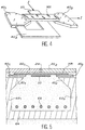
- the invention applies essentially to heads say horizontal with thin layers. Such a head is shown in Figure 1 attached.
- a head comprising a semiconductor substrate 10, for example made of silicon, in which a box 12 has been etched.
- a lower magnetic layer 14 has been formed, for example electrolytically, and has been extended by two vertical studs 16 1 16 2 .
- a conductive winding 18 surrounds the pads. It is embedded in an insulating layer 20.
- the magnetic circuit is completed by an upper magnetic layer separated into two pole pieces 22 1 , 22 2 held apart by a non-magnetic spacer 24 forming an air gap.
- a magnetoresistive MR element made of material monolithic (for example in Fe-Ni), is placed under the non-magnetic spacer 24.
- the head moves in front of a magnetic support 30 where the information to read or write.
- Such a head is described in the document FR-A-2 657 189.
- this head is schematically the following.
- the current flowing in the winding 18 creates a magnetic field and therefore an induction in the circuit magnetic.
- Flourishing field lines around the spacer 24 induce a magnetization in the support 30.
- the width of the track to be read becomes small.
- the length of the magnetoresistance (counted in the direction transverse, that is to say perpendicular to the track) becomes of the order of a few microns (for example 3 ⁇ m) which is precisely the order of magnitude the width of the magnetoresistance (2 to 3 ⁇ m).
- the magnetoresistance takes a substantially square shape with very small dimensions. It is then very difficult to obtain a resistance adapted to the circuit detection, resistance which is generally around 50 Ohms, which would require a layer much too thin to be usable.
- the purpose of the present invention is to remedy this drawback.
- Document JP-B-286,413 describes a device analog with only two pole pieces substantially flat and separated by an air gap. A magnetoresistive element is placed just under the air gap, all resting on a substrate. This magnetoresistive element operates in transverse, as in the head described in FR-A-2 657 189 already cited.
- the magnetoresistant element is therefore very distant from the main air gap.
- this element being in contact with the pole pieces, it forms a real second magnetic circuit.
- EP-0 652 550 which is a statement of the technique according to Article 54 (3) EPC, describes a head magnetic reading with magnetoresistive element multilayer but whose pole pieces are not flat.
- EP-0 702 358 describes a head magnetic with multilayer magnetoresistance with a magnetic layer deposited on two inclined sides.
- the invention retains the provision of place the magnetoresistive element just under the air gap. But the invention proposes, on the one hand, to use, as a magnetoresistant element, a magnetoresistance of a particular type, namely multilayer type (and no longer monolithic) and, on the other part, to operate this magnetoresistance in longitudinal mode (and no longer transverse).
- magnetoresistant materials multilayers consist of a stack of layers magnetic separated by metallic layers not magnetic.
- Multilayer metallic structures use cobalt, iron, copper, chromium, nickel, alloys of iron and nickel, silver, gold, molybdenum, ruthenium and manganese, as described in the article by H. YAMAMOTO and T. SHINJO, published in the journal “IEEE Translation Journal on Magnetics in Japan “, vol. 7, n ° 9, September 1992, under the title “Magnetoresistance of Multilayers", p. 674-684).
- Such an element can operate in longitudinal if the measurement current flowing through it and the magnetic field it detects are collinear and directed lengthwise of the element.
- a multilayer magnetoresistor used in longitudinal is either "spin valve” or antiferromagnetic coupling (i.e. in the field null, the magnetic layers present alternately opposite magnetization).
- the invention applies more particularly to the latter type of magnetoresistance.
- the use of a multilayer magnetoresistance allows close coupling between the two upper pole pieces of the head and the magnetoresistance. Like the magnetic flux going through the magnetoresistance is in the same direction of the current running through it, this meaning being that of the longitudinal direction of the element, the effect of demagnetizing fields is reduced and, as a result, the head sensitivity is increased.
- the present invention therefore for object a magnetic reading head comprising a magnetic circuit comprising two pole pieces separated by an air gap and a magnetoresistive tape dish consisting of a multilayer magnetoresistance and arranged under the pole pieces and under the air gap, characterized in that the magnetic circuit consists only of the two pole pieces and includes only a single air gap, said parts polar being planar, the head thus being planar, the flat magnetoresistive tape including a stack of magnetic layers separated by layers non-magnetic metal, this magnetoresistance extending longitudinally under the pole pieces and under the single air gap and working in fashion longitudinal.
- Figure 2 shows, in section, a mode of realization of a magnetic reading head according to the invention. In this figure, we find elements
- FIG. 2 shows, in section, an embodiment of a magnetic reading head according to the invention.
- the magnetoresistive element MR is of the multilayer and longitudinal type and has the shape of a substantially flat ribbon. This strip is connected to two electrical contacts 40 1 , 40 2 . These contacts and a current generator (not shown) make it possible to circulate a current I in the longitudinal resistance in the longitudinal direction.
- the head still includes a bias conductor 50 arranged transversely (perpendicular to the plane of the figure).
- Figure 3 shows these same means but in top view. You can see the flared shape of the electrical contacts 40 1 , 40 2 and the transverse direction of the conductor 50.
- the distance d between the contacts 40 1 , 40 2 fixes the electrical length of the magnetoresistor. This length is adjusted so as to obtain a maximum coupling between the poles 22 1 and 22 2 and a maximum signal taking into account the width of the track. It is generally between 2 and 20 ⁇ m depending on the width of the track; for example, it is around 8 ⁇ m for a 5 ⁇ m track.
- the width H of the magnetoresistor MR is determined as a function of the distance e separating the magnetoresistance from the pole pieces 22 1 , 22 2 . It is of the order of the width TW of the pole pieces, possibly slightly lower or slightly greater.
- the width TW of the pole pieces can be of the order of 2 ⁇ m and the width H of the order of 3 ⁇ m.
- the longitudinal current I which flows through the magnetoresistance creates a magnetic field winding around the current lines and directed, therefore, perpendicular to the plane of Figure 2, at the two pole pieces 22 1 , 22 2 .
- This field has the effect of stabilizing the magnetic domains in said pole pieces.
- the bias conductor 50 may be in CrAu, TaAu, TiW or TiWAu. This driver can possibly include a thin magnetic layer, in order to increase its efficiency.
- FIG. 4 illustrates a particular embodiment of the magnetoresistor MR and of the bias conductor 50.
- the two elements are connected in series by means of a connection element 40 3 connected to the end contact 40 1 .
- the current I which flows in the magnetoresistor MR also flows in the conductive element 50 serving for the polarization of the magnetoresistor.
- the bias conductor 50 is advantageously made of the same material than magnetoresistance. So it too can be magnetoresistive. Naturally, it will be an effect transverse rather than longitudinal magnetoresistive as in the main magnetoresistance MR. However, this side effect, linked to the magnetic flux which will not passed through the main magnetoresistance MR but will partially recovered by the conductive element, will improve the overall sensitivity of the head.
- the head which has just been described is used only for reading magnetic information. In others terms, this is a sensor. We can complete the device described to make it, moreover, suitable for writing information on a medium. We will get then a read and write head.
- Such a head is shown, in section, in FIG. 5.
- the elements already represented in FIGS. 2 and 3 bear the same references, namely the two pole pieces 22 1 , 22 2 , the non-magnetic gap 24, the magnetoresistance MR , the contacts 40 1 , 40 2 and the bias conductor 50.
- the head shown comprises, in addition, a magnetic circuit for closing the flux, which is constituted, in the example illustrated, by two concentrators 60 1 , 60 2 , two pillars 62 1 , 62 2 and an inner magnetic layer 64.
- the device also includes a winding conductor 68 coupled to the magnetic circuit. It's about usually a double spiral winding. It's at through this winding that flows the current writing.
- the MR magnetoresistance is not not in electrical contact with the closing circuit of the flux but its ends are arranged in this circuit. During the writing phase, the ends of the magnetoresistance will be saturated by the field of writing which will not hinder writing.
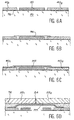
- Figures 6A to 6D show four stages of a process for producing a read head according to the invention (or the upper part of a reading and writing).
- a substrate 70 or of a sub-assembly already comprising a closing of the flow with its winding. So substrate, an insulating layer 72 is deposited (FIG. 6A).
- a metallic layer is then deposited which is etched into three elements, a central element 50 which will constitute the future bias conductor and two end elements 40 1 , 40 2 which will form the future contact pads.
- An insulating layer 74 is then deposited (FIG. 6B) that we engrave in order to let it subsist only center.
- a new insulating layer 76 is deposited (FIG. 6D) and the pole pieces 22 1 , 22 2 separated by the non-magnetic gap 24 are formed by any known means.
Landscapes
- Engineering & Computer Science (AREA)
- Manufacturing & Machinery (AREA)
- Chemical & Material Sciences (AREA)
- Nanotechnology (AREA)
- Crystallography & Structural Chemistry (AREA)
- Physics & Mathematics (AREA)
- Mathematical Physics (AREA)
- Theoretical Computer Science (AREA)
- Magnetic Heads (AREA)
Claims (6)
- Lesemagnetkopf mit einem Magnetkreis, der zwei durch einen Spalt (24) getrennte Polschuhe (221, 222) und einen ebenen bzw. flachen, unter den Polschuhen (221, 222) und unter dem Spalte (24) angeordneten und durch eine magnetoresistente Schicht gebildeten magnetoresistenten Streifen (MR) umfasst,
dadurch gekennzeichnet,
dass der Magnetkreis nur durch die beiden Polschuhe (221, 222) gebildet wird und nur einen einzigen Spalt umfasst, wobei die genannten Polschuhe eben sind, der Kopf somit planar ist und der ebene magnetoresistive Streifen (MR) einen Stapel magnetischer Schichten umfasst, die durch unmagnetische metallische Schichten getrennt sind, und diese Magnetoresistenz sich longitudinal unter den Polschuhen (221, 222) und unter dem einzigen Spalt (24) erstreckt und im Longitudialmodus arbeitet. - Planarer Magnetkopf nach Anspruch 1, der außerdem zwei elektrische Kontakte (401, 402) an den beiden Enden der Magnetoresistenz (MR) umfasst.
- Planarer Magnetkopf nach Anspruch 1, der außerdem einen quer angeordneten Polarisationsleiter (50) umfasst.
- Planarer Magnetkopf nach Anspruch 3, bei dem der Polarisationsleiter (50) elektrisch mit dem magnetoresistiven Streifen (MR) in Serie geschaltet ist.
- Planarer Magnetkopf nach Anspruch 4, bei dem der Polarisationsleiter (50) ein magnetoresistives Material ist.
- Lese-Schreibmagnetkopf mit einem Lesemagnetkopf nach Anspruch 1 und außerdem einem den Magnetfluss schließenden Magnetkreis (601, 602, 621, 622, 64) und einer magnetisch mit dem Magnetkreis gekoppelten leitende Wicklung (68), wobei der Kopf sowohl lesen als auch schreiben kann und die Magnetoresistenz (MR) nicht in Kontakt mit dem den Magnetfluss schließenden Magnetkreis ist, sondern ihre Enden in dem genannten, den Magnetfluss schließenden Magnetkreis angeordnet sind.
Applications Claiming Priority (3)
| Application Number | Priority Date | Filing Date | Title |
|---|---|---|---|
| FR9410895A FR2724481B1 (fr) | 1994-09-13 | 1994-09-13 | Tete magnetique planaire a magnetoresistance multicouche longitudinale |
| FR9410895 | 1994-09-13 | ||
| PCT/FR1995/001168 WO1996008814A1 (fr) | 1994-09-13 | 1995-09-12 | Tete magnetique planaire a magnetoresistance multicouche longitudinale |
Publications (2)
| Publication Number | Publication Date |
|---|---|
| EP0781448A1 EP0781448A1 (de) | 1997-07-02 |
| EP0781448B1 true EP0781448B1 (de) | 2000-02-16 |
Family
ID=9466884
Family Applications (1)
| Application Number | Title | Priority Date | Filing Date |
|---|---|---|---|
| EP95930575A Expired - Lifetime EP0781448B1 (de) | 1994-09-13 | 1995-09-12 | Planarer magnetkopf mit longitudinalem mehrschichtmagnetowiderstand |
Country Status (6)
| Country | Link |
|---|---|
| US (1) | US5910869A (de) |
| EP (1) | EP0781448B1 (de) |
| JP (1) | JPH10507862A (de) |
| DE (1) | DE69515123T2 (de) |
| FR (1) | FR2724481B1 (de) |
| WO (1) | WO1996008814A1 (de) |
Families Citing this family (12)
| Publication number | Priority date | Publication date | Assignee | Title |
|---|---|---|---|---|
| US6198607B1 (en) * | 1995-12-22 | 2001-03-06 | Censtor Corporation | Contact planar magnetoresistive head |
| JPH1098220A (ja) * | 1996-09-20 | 1998-04-14 | Sanyo Electric Co Ltd | 磁気抵抗効果素子 |
| FR2761477B1 (fr) * | 1997-04-01 | 1999-04-23 | Commissariat Energie Atomique | Capteur de champ magnetique a magnetoresistance |
| FR2774500B1 (fr) * | 1998-02-03 | 2000-04-07 | Silmag Sa | Tete magnetique de lecture a element magnetoresistant et a element conducteur de compensation |
| US6525913B1 (en) | 2000-08-09 | 2003-02-25 | International Business Machines Corporation | Read head with sunken prefill insulation for preventing lead to shield shorts and maintaining planarization |
| KR100438341B1 (ko) * | 2000-09-26 | 2004-07-02 | 가부시끼가이샤 도시바 | 요크형 재생 자기 헤드 및 그 제조 방법, 및 자기 디스크장치 |
| US20080068750A1 (en) * | 2006-09-19 | 2008-03-20 | International Business Machines Corporation | Planar Write Module And Hybrid Planar Write-Vertical Read Bidirectional Tape Head |
| US20080068752A1 (en) * | 2006-09-19 | 2008-03-20 | International Business Machines Corporation | Planar Bidirectional Tape Head With Planar Read And Write Elements |
| US8711524B2 (en) * | 2008-02-05 | 2014-04-29 | Headway Technologies, Inc. | Patterned MR device with controlled shape anisotropy |
| US8240024B2 (en) * | 2009-08-25 | 2012-08-14 | International Business Machines Corporation | Methods for fabricating magnetic transducers using post-deposition tilting |
| US8351152B2 (en) | 2009-08-25 | 2013-01-08 | International Business Machines Corporation | Magnetic writer structures formed using post-deposition tilting |
| US8416537B2 (en) * | 2009-11-06 | 2013-04-09 | International Business Machines Corporation | Recording head with tilted orientation |
Citations (2)
| Publication number | Priority date | Publication date | Assignee | Title |
|---|---|---|---|---|
| EP0652550A1 (de) * | 1993-11-08 | 1995-05-10 | Commissariat A L'energie Atomique | Lesemagnetkopf mit Mehrschichtmagnetowiderstandselement und Konzentrator und Herstellungsverfahren |
| EP0702358A1 (de) * | 1994-09-13 | 1996-03-20 | Commissariat A L'energie Atomique | Magnetkopf mit unterliegendem longitudinalem Mehrschicht-Magnetowiderstand |
Family Cites Families (10)
| Publication number | Priority date | Publication date | Assignee | Title |
|---|---|---|---|---|
| FR2455330A1 (fr) * | 1979-04-25 | 1980-11-21 | Cii Honeywell Bull | Dispositif magnetique de transduction a magnetoresistances |
| JPS63266619A (ja) * | 1987-04-23 | 1988-11-02 | Sharp Corp | 薄膜磁気ヘツド |
| JPH0328643A (ja) * | 1989-06-27 | 1991-02-06 | Matsushita Electric Works Ltd | 空気清浄システム |
| FR2657189B1 (fr) * | 1990-01-18 | 1993-12-31 | Commissariat A Energie Atomique | Tete magnetique de lecture et d'ecriture a element magnetoresistant. |
| JPH03286413A (ja) * | 1990-04-02 | 1991-12-17 | Matsushita Electric Ind Co Ltd | 磁気抵抗郊果型ヘッド |
| US5274521A (en) * | 1990-08-23 | 1993-12-28 | Sony Corporation | Planar thin film magnetic head |
| JP3200060B2 (ja) * | 1990-09-12 | 2001-08-20 | ソニー株式会社 | 薄膜磁気ヘッド |
| JP2812042B2 (ja) * | 1992-03-13 | 1998-10-15 | 松下電器産業株式会社 | 磁気抵抗センサー |
| US5287238A (en) * | 1992-11-06 | 1994-02-15 | International Business Machines Corporation | Dual spin valve magnetoresistive sensor |
| US5301079A (en) * | 1992-11-17 | 1994-04-05 | International Business Machines Corporation | Current biased magnetoresistive spin valve sensor |
-
1994
- 1994-09-13 FR FR9410895A patent/FR2724481B1/fr not_active Expired - Fee Related
-
1995
- 1995-09-12 JP JP8509952A patent/JPH10507862A/ja active Pending
- 1995-09-12 DE DE69515123T patent/DE69515123T2/de not_active Expired - Fee Related
- 1995-09-12 EP EP95930575A patent/EP0781448B1/de not_active Expired - Lifetime
- 1995-09-12 US US08/793,894 patent/US5910869A/en not_active Expired - Fee Related
- 1995-09-12 WO PCT/FR1995/001168 patent/WO1996008814A1/fr not_active Ceased
Patent Citations (2)
| Publication number | Priority date | Publication date | Assignee | Title |
|---|---|---|---|---|
| EP0652550A1 (de) * | 1993-11-08 | 1995-05-10 | Commissariat A L'energie Atomique | Lesemagnetkopf mit Mehrschichtmagnetowiderstandselement und Konzentrator und Herstellungsverfahren |
| EP0702358A1 (de) * | 1994-09-13 | 1996-03-20 | Commissariat A L'energie Atomique | Magnetkopf mit unterliegendem longitudinalem Mehrschicht-Magnetowiderstand |
Also Published As
| Publication number | Publication date |
|---|---|
| US5910869A (en) | 1999-06-08 |
| FR2724481A1 (fr) | 1996-03-15 |
| EP0781448A1 (de) | 1997-07-02 |
| FR2724481B1 (fr) | 1996-10-18 |
| DE69515123T2 (de) | 2000-09-21 |
| WO1996008814A1 (fr) | 1996-03-21 |
| JPH10507862A (ja) | 1998-07-28 |
| DE69515123D1 (de) | 2000-03-23 |
Similar Documents
| Publication | Publication Date | Title |
|---|---|---|
| EP0418372B1 (de) | Lese-magnetkopf mit magnetowiderstand für senkrechte aufzeichnung und herstellungsverfahren eines derartigen kopfes | |
| EP0724302B1 (de) | Magnetsensor mit einem Riesenmagnetowiderstand und sein Herstellungsverfahren | |
| EP0284495B1 (de) | Magnetkopf zum Lesen von Spuren mit sehr schmaler Breite und Herstellungverfahren | |
| EP0652550B1 (de) | Lesemagnetkopf mit Mehrschichtmagnetowiderstandselement und Konzentrator und Herstellungsverfahren | |
| EP0781448B1 (de) | Planarer magnetkopf mit longitudinalem mehrschichtmagnetowiderstand | |
| EP0693791B1 (de) | Magnetwiderstands-Sensor mit selbstpolarisiertem Mehrschichtsystem | |
| KR19990036652A (ko) | 자속 가이드로서의 감지층을 갖는 자기 터널 접합부 자기 저항판독 헤드 | |
| EP0467736B1 (de) | Magnetoresistiver Effekt verwendender Lesemagnetkopf | |
| EP0853766A1 (de) | Magnetfeldsensor mit einer magnetowiderstandsbrücke | |
| FR2645314A1 (fr) | Tete magnetique a magnetoresistance pour enregistrement longitudinal et procede de realisation d'une telle tete | |
| FR2652669A1 (fr) | Procede de realisation d'une tete d'enregistrement magnetique et tete obtenue par ce procede. | |
| FR2724482A1 (fr) | Tete magnetique a magnetoresistance multicouche longitudinale sous-jacente | |
| FR2817622A1 (fr) | Micromagnetometre a porte de flux | |
| FR2511535A1 (fr) | Tete de transducteur magnetique | |
| EP0642181B1 (de) | Magnetoresistive Anordnung und Fühler mit wiederholenden geometrischen Strukturen | |
| EP0497069B1 (de) | Herstellungsverfahren von magnetoresistiven Sensoren und nach diesem Verfahren hergestellte magnetische Vorrichtung | |
| FR2709855A1 (fr) | Tête magnétique de lecture et d'écriture à élément magnétorésistant compensé en écriture. | |
| FR2496952A1 (fr) | Tete de transducteur magnetique a effet de magneto-resistance | |
| EP0658772B1 (de) | Magnetischer Fühler mit magnetoresistivem Effekt | |
| EP0669609B1 (de) | Lesemagnetkopf mit magnetoresistivem Element und verbesserten Vormagnetisierungsmitteln | |
| FR2802011A1 (fr) | Tete de lecture planaire a element magneto-resistif | |
| FR2769399A1 (fr) | Tete magnetique avec une partie lecture et une partie ecriture | |
| FR2676301A1 (fr) | Tete magnetique d'ecriture et de lecture a largeur de poles dissymetrique. | |
| FR2493015A1 (fr) | Transducteur magnetoresistant | |
| FR2772965A1 (fr) | Senseur de champ magnetique et tete magnetique de lecture utilisant un tel senseur |
Legal Events
| Date | Code | Title | Description |
|---|---|---|---|
| PUAI | Public reference made under article 153(3) epc to a published international application that has entered the european phase |
Free format text: ORIGINAL CODE: 0009012 |
|
| 17P | Request for examination filed |
Effective date: 19970218 |
|
| AK | Designated contracting states |
Kind code of ref document: A1 Designated state(s): DE FR GB IT |
|
| 17Q | First examination report despatched |
Effective date: 19970728 |
|
| GRAG | Despatch of communication of intention to grant |
Free format text: ORIGINAL CODE: EPIDOS AGRA |
|
| GRAG | Despatch of communication of intention to grant |
Free format text: ORIGINAL CODE: EPIDOS AGRA |
|
| GRAH | Despatch of communication of intention to grant a patent |
Free format text: ORIGINAL CODE: EPIDOS IGRA |
|
| GRAH | Despatch of communication of intention to grant a patent |
Free format text: ORIGINAL CODE: EPIDOS IGRA |
|
| GRAA | (expected) grant |
Free format text: ORIGINAL CODE: 0009210 |
|
| AK | Designated contracting states |
Kind code of ref document: B1 Designated state(s): DE FR GB IT |
|
| REF | Corresponds to: |
Ref document number: 69515123 Country of ref document: DE Date of ref document: 20000323 |
|
| ITF | It: translation for a ep patent filed | ||
| GBT | Gb: translation of ep patent filed (gb section 77(6)(a)/1977) |
Effective date: 20000428 |
|
| EN | Fr: translation not filed | ||
| PG25 | Lapsed in a contracting state [announced via postgrant information from national office to epo] |
Ref country code: FR Free format text: LAPSE BECAUSE OF FAILURE TO SUBMIT A TRANSLATION OF THE DESCRIPTION OR TO PAY THE FEE WITHIN THE PRESCRIBED TIME-LIMIT Effective date: 20000713 |
|
| EN4 | Fr: notification of non filing translation in an earlier bopi is erroneous | ||
| REG | Reference to a national code |
Ref country code: FR Ref legal event code: TP |
|
| PLBE | No opposition filed within time limit |
Free format text: ORIGINAL CODE: 0009261 |
|
| STAA | Information on the status of an ep patent application or granted ep patent |
Free format text: STATUS: NO OPPOSITION FILED WITHIN TIME LIMIT |
|
| 26N | No opposition filed | ||
| REG | Reference to a national code |
Ref country code: GB Ref legal event code: IF02 |
|
| PGFP | Annual fee paid to national office [announced via postgrant information from national office to epo] |
Ref country code: GB Payment date: 20020911 Year of fee payment: 8 |
|
| PGFP | Annual fee paid to national office [announced via postgrant information from national office to epo] |
Ref country code: DE Payment date: 20020923 Year of fee payment: 8 |
|
| PGFP | Annual fee paid to national office [announced via postgrant information from national office to epo] |
Ref country code: FR Payment date: 20020930 Year of fee payment: 8 |
|
| PG25 | Lapsed in a contracting state [announced via postgrant information from national office to epo] |
Ref country code: GB Free format text: LAPSE BECAUSE OF NON-PAYMENT OF DUE FEES Effective date: 20030912 |
|
| PG25 | Lapsed in a contracting state [announced via postgrant information from national office to epo] |
Ref country code: DE Free format text: LAPSE BECAUSE OF NON-PAYMENT OF DUE FEES Effective date: 20040401 |
|
| GBPC | Gb: european patent ceased through non-payment of renewal fee |
Effective date: 20030912 |
|
| REG | Reference to a national code |
Ref country code: FR Ref legal event code: ST |
|
| PG25 | Lapsed in a contracting state [announced via postgrant information from national office to epo] |
Ref country code: IT Free format text: LAPSE BECAUSE OF NON-PAYMENT OF DUE FEES;WARNING: LAPSES OF ITALIAN PATENTS WITH EFFECTIVE DATE BEFORE 2007 MAY HAVE OCCURRED AT ANY TIME BEFORE 2007. THE CORRECT EFFECTIVE DATE MAY BE DIFFERENT FROM THE ONE RECORDED. Effective date: 20050912 |