EP0468116B1 - Détecteur de signaux - Google Patents
Détecteur de signaux Download PDFInfo
- Publication number
- EP0468116B1 EP0468116B1 EP90313744A EP90313744A EP0468116B1 EP 0468116 B1 EP0468116 B1 EP 0468116B1 EP 90313744 A EP90313744 A EP 90313744A EP 90313744 A EP90313744 A EP 90313744A EP 0468116 B1 EP0468116 B1 EP 0468116B1
- Authority
- EP
- European Patent Office
- Prior art keywords
- light
- light receiving
- electrodes
- electrode
- information recording
- Prior art date
- Legal status (The legal status is an assumption and is not a legal conclusion. Google has not performed a legal analysis and makes no representation as to the accuracy of the status listed.)
- Expired - Lifetime
Links
Images

Classifications
-
- G—PHYSICS
- G11—INFORMATION STORAGE
- G11B—INFORMATION STORAGE BASED ON RELATIVE MOVEMENT BETWEEN RECORD CARRIER AND TRANSDUCER
- G11B7/00—Recording or reproducing by optical means, e.g. recording using a thermal beam of optical radiation by modifying optical properties or the physical structure, reproducing using an optical beam at lower power by sensing optical properties; Record carriers therefor
- G11B7/12—Heads, e.g. forming of the optical beam spot or modulation of the optical beam
- G11B7/13—Optical detectors therefor
- G11B7/131—Arrangement of detectors in a multiple array
-
- G—PHYSICS
- G11—INFORMATION STORAGE
- G11B—INFORMATION STORAGE BASED ON RELATIVE MOVEMENT BETWEEN RECORD CARRIER AND TRANSDUCER
- G11B7/00—Recording or reproducing by optical means, e.g. recording using a thermal beam of optical radiation by modifying optical properties or the physical structure, reproducing using an optical beam at lower power by sensing optical properties; Record carriers therefor
- G11B7/08—Disposition or mounting of heads or light sources relatively to record carriers
- G11B7/09—Disposition or mounting of heads or light sources relatively to record carriers with provision for moving the light beam or focus plane for the purpose of maintaining alignment of the light beam relative to the record carrier during transducing operation, e.g. to compensate for surface irregularities of the latter or for track following
- G11B7/0943—Methods and circuits for performing mathematical operations on individual detector segment outputs
Definitions
- This invention relates to a signal detector used for an information recording/reproduction device and more particularly to the signal detector in which an element for detecting a signal is easily assembled.
- a type of conventional signal detector has a semiconductor laser for emitting laser light, a beam splitter through which laser light from the semiconductor laser travels to an optical disk and which splits signal light reflected and diffracted by the optical disk, an objective lens for condensing and projecting the laser light transmitted through the beam splitter to an information recording surface of the optical disk, a biprism for separating the signal light split by the beam splitter into two beams, and a photodetector device which has a plurality of photodiodes for receiving the two beams of signal light separated by the biprism and which detects an error in focusing on the optical disk.
- Laser light emitted from the semiconductor laser is projected to the information recording surface of the optical disk by the condensing effect of the optical system.
- the projected laser light is reflected and diffracted by the information recording surface of the optical disk to form signal light.
- This signal light is separated into two beams of light by the biprism, and these two beams of light are received by the photodiodes of the photodetector device bisectionally arranged.
- Defocus detection is effected based on the Foucault method using signals output from the photodiodes receiving the light to obtain a focus error signal.
- the signal detector in accordance with the prior art entails a problem in that the photodiodes of the photodetector device and the biprism must be attached with a high accuracy while moving and adjusting the attached positions so that the beams of signal light condensed and projected at the time of focusing are correctly condensed to the photodiode division lines. Also, in a case where attachment adjustment is not effected, it is necessary to separately provide an error correction circuit.
- a signal detector for optically detecting a signal from an information recording medium onto which an information is recorded or from which said information is reproduced, which comprises: at least one light receiving element for receiving light from said information recording medium which is irradiated with light for recording or reproduction, said light receiving element having a light receiving surface for receiving the light from said information recording medium; and a plurality of electrodes arranged in positions opposite to said light receiving surface, information recording/reproduction being effected based on a detection signal output from said light receiving element,connection for one of said electrodes opposite to a point on said light receiving surface at which the light from said information recording medium is incident upon said light receiving surface being cut to separate said plurality of electrodes into two divided electrode regions on the opposite sides of said disconnected electrode with respect to the cut electrode, focus control being effected based on detection signals output from the two electrode regions.
- a plurality of electrodes are arranged opposite to the surface of the light receiving element through which light is received, and the electrode opposite to the position of incidence of the received light is cut off to form two electrode regions on the opposite sides of the electrode cut off and to set a virtual division line.
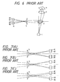
- the conventional signal detector has a semiconductor laser 1 for emitting laser light, a beam splitter 2 through which laser light from the semiconductor laser 1 travels to an optical disk 4 and which splits signal light reflected and diffracted by the optical disk 4, an objective lens 3 for condensing and projecting the laser light transmitted through the beam splitter 2 onto an information recording surface of the optical disk 4, a biprism 5 for separating the signal light split by the beam splitter 2 into two beams, and a photodetector device 6 which has photodiodes 61 to 64 for receiving the two beams of signal light separated by the biprism 5 and which detects an error in focusing on the optical disk 4.
- Laser light emitted from the semiconductor laser 1 travels through the beam splitter 2 and is projected to the information recording surface of the optical disk 4 by the condensing effect of the objective lens 3.
- the projected laser light is reflected and diffracted to form signal light by the information recording surface of the optical disk 4.
- This signal light is split by the beam splitter 2 through the objective lens 3.
- the signal light split thereby is separated into two beams of light by the biprism 5, and these two beams of light are received by the photodiodes 61 to 64 of the photodetector device 6 bisectionally arranged.
- the four photodiodes 61 to 64 and the biprism 5 must be assembled at their correct positions. After these members are assembled one, it is very troublesome to adjust the positional relationship between those members. This defect can be eliminated by this invention.
- a signal detector comprises at least one light receiving element for receiving light from an information recording medium on which various categories of information are recorded and which is irradiated with light for recording or reproduction.
- the light receiving element has a light receiving surface for receiving the light from the information recording medium and a plurality of electrodes arranged in positions opposite to the light receiving surface.
- Information recording/reproduction is effected based on a detection signal output from the light receiving element.
- Connection for one of the electrodes opposite to a point on the light receiving surface at which the light from the information recording medium is incident on the light receiving surface is cut to separate the plurality of electrodes with respect to two divided electrode regions or groups (A, B) on the opposite sides of the disconnected electrode. Focusing control is effected based on detection signals output from the two electrode regions.
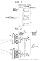
- Fig. 2 is a diagram of an essential portion of the embodiment of the present invention
- Fig. 3 is a plan view of the semiconductor substrate of the embodiment
- Fig. 4 is an enlarged cross-sectional view taken along the line A - A of Fig. 3.
- a signal detector D in accordance with the embodiment has an optical separator 20 and a diffraction grating 50, a pair of photodiodes 6A and 6B, and a laser trimming section 12.
- the optical separator 20 is placed on a semiconductor substrate 10 to reflect laser light from a semiconductor laser 1 by its side surface 21 to make the reflected light travel to an optical disk 4. Also, the light diffracted and reflected by the optical disk 4 is incident upon the side surface of the optical separator 20 to be emergent through another side surface 22 of the same.
- the diffraction grating 50 is formed between a clad layer 16 and an optical waveguide layer 15 on the semiconductor substrate 10 to separate the signal light emergent from the side surface 22 of the optical separator 20 into two beams and to introduce the same into the optical waveguide layer 17.
- the photodiodes 6A and 6B are formed at an end surface of the optical waveguide layer 17 to receive the two beams of signal light through signal receiving surfaces 67A and 67B.
- the photodiodes 6A and 6B output signals corresponding to the received signal light through two arrays of electrodes each consisting of six electrodes 61a to 66a or 61b to 66b positioned opposite to the light receiving surface 67A or 67B.
- the laser trimming section 12 effects laser trimming by selecting connection lines from the electrodes 61a to 66a, and 61b to 66b of the photodiodes 6A and 6B.
- each photodiode 6A or 6B is grouped into two regions, and the group of electrodes 61a to 63a or 61b to 63b and the group of electrodes 64a to 66a or 64b to 66b are respectively connected in the laser trimming section 12.
- Elements or components other than the laser trimming section 12 are also formed on the semiconductor substrate 10, including attachment lands 1a and 1b on which the semiconductor layer 1 is connected and mounted, an electric circuit section 13 for controlling the output from the semiconductor laser 1 and for calculation using signals output from the photodiodes 6A and 6B, and bonding pads 14 used for wire bonding connection to an external unit.
- laser light emitted from the semiconductor laser 1 is reflected by the optical separator 20 on the side of the same closer to the semiconductor laser 1 to travel to the optical disk 4.
- This reflection light is diffracted and reflected by the information recording surface of the optical disk 4 and is thereby changed into a signal light.
- This signal light is incident upon the side surface 21 of the optical separator 20, passes through this surface, and is emergent through the side surface 22.
- This emergent signal light is separated into two beams by the diffraction grating 50 and each of the two beams of light separated is received by the photodiode 6A or 6B.
- photodiode 6A or 6B When photons of the light received are incident upon the substrate of the photodiode 6A and 6B, electrons in the substrate are excited and a current is thereby output through the electrode located in the vicinity of the incidence point.
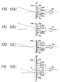
- connection lines from the electrodes 64a and 63b opposite to the points A and B on the light receiving surfaces 67A and 67B of the photodiodes 6A and 6B are cut off by the laser trimming section 12.
- connection line cutting virtual photodiode division lines are set at the points A and B of the photodiodes 6A and 6B, respectively.
- adders 13a, 13b, and 13c of the electric circuit 13 operate for calculation based on the Foucault method as described below. That is, if signals output from the electrodes 61a to 66a, and 61b to 66b are S61a to S66a, and S61b to S 66b, calculation of (S 61a + S 62a + S 63a + S 64b + S 65b + S 66b ) - (S 65a + S 66a + S 61b + S 62b ) is effected. If the focus detection signal obtained from the result of this calculation is zero, a focused state is detected. If the focus detection signal has a positive value, a state in which the optical disk 4 is remoter is detected, or if the focus detection signal has a negative value, a state in which the optical disk is nearer is detected.
- the output from the adder 13a has a negative value
- laser trimming is effected by cutting the connection line from the electrode 64a
- a virtual photodiode division line is set at the point on the light receiving surface 67A of the photodiode 6A opposite to the electrode 64a.
- the number of electrodes may be freely selected so long as it is not smaller than three. Specifically, the adjustment sensitivity can be improved if the number of electrodes is increased or if the intervals between the electrodes are reduced.
- each divided group of electrodes has, for example, four electrodes 61a to 64a or 65a to 68a and where the light is incidint at a point opposite to an electrode 66a deviated over the electrode 65a from a boundary between two groups each having four electrodes which are connected one another, connection is cut with respect to the two electrodes 65a, 66a.
- the intervals between the electrodes may be set to be smaller than the minimum diameter of the spot of light incident upon the light receiving surface of each light receiving element to improve the accuracy with which the virtual division line is adjusted.
- the embodiment has been described with respect to an example of two-dimensional adjustment.
- the present invention can also be applied to three-dimensional adjustment of photodiodes of a discrete pickup.
- a plurality of electrodes are arranged opposite to the surface of the light receiving element through which light is received, and the electrode opposite to the position of incidence of the received light is cut off to form two electrode regions on the opposite sides of the electrode cut off, thereby setting a virtual division line.
- the need for the provision of a structural division line on the light receiving element used for focusing control is thereby eliminated. Therefore there is no need for strict adjustment of the attachment position and, hence, no need for an error adjustment circuit separately provided for adjustment.
Landscapes
- Physics & Mathematics (AREA)
- Mathematical Physics (AREA)
- Optics & Photonics (AREA)
- Optical Recording Or Reproduction (AREA)
- Optical Head (AREA)
Claims (6)
- Détecteur de signaux pour détecter optiquement un signal à partir d'un support d'enregistrement d'informations sur lequel des informations sont enregistrées ou à partir duquel lesdites informations sont reproduites, ledit détecteur de signaux comprenant au moins un élément récepteur de lumière (67A, 67B) pour recevoir de la lumière provenant dudit support d'enregistrement d'informations qui est illuminé avec de la lumière pour l'enregistrement ou la reproduction, ledit élément récepteur de lumière (67A, 67B) ayant une surface réceptrice de lumière pour recevoir la lumière provenant dudit support d'enregistrement d'informations, et une pluralité d'électrodes (61a à 66a, 61b à 66b), l'enregistrement et la reproduction d'informations étant effectués sur la base d'un signal de détection fourni par ledit élément récepteur de lumière, caractérisé en ce que ladite pluralité d'électrodes est disposée à des positions faisant face à ladite surface réceptrice de lumière, une connexion d'une desdites électrodes faisant face à un point situé sur ladite surface réceptrice de lumière auquel la lumière provenant dudit support d'enregistrement d'informations est incidente sur ladite surface réceptrice de lumière (67A, 67B) étant coupée pour diviser ladite pluralité d'électrodes (61a à 66a, 61b à 66b) en deux régions d'électrodes divisées sur les côtés opposés de l'électrode déconnectée par rapport à l'électrode coupée, la commande de la focalisation étant basée sur des signaux de détection fournis à partir des deux régions d'électrodes.
- Détecteur de signaux selon la revendication 1, dans lequel ladite pluralité d'électrodes (61a à 66a, 61b à 66b) dudit élément récepteur de lumière (67A, 67B) sont préalablement groupées en deux régions divisées et une pluralité d'électrodes (61a à 66a, 61b à 66b) dans chaque région divisée ainsi formée sont respectivement connectées, et dans lequel, si la lumière réfléchie par ledit support d'enregistrement d'informations, dans un état dans lequel un système optique est focalisé, est incidente sur la surface réceptrice de lumière dudit élément récepteur de lumière (67A, 67B) tout en étant décalée d'une frontière entre les régions divisées, la connexion de chacune des électrodes allant de l'électrode faisant face au point d'incidence de la lumière décalée sur la surface réceptrice de lumière à l'électrode correspondant à la frontière de la région divisée, est coupée.
- Détecteur de signaux selon la revendication 1, dans lequel la lumière provenant dudit support d'enregistrement d'informations est divisée en deux faisceaux, et deux éléments récepteurs de lumière (67A, 67B) sont prévus pour recevoir respectivement les faisceaux de lumière ainsi divisée.
- Détecteur de signaux selon la revendication 1, dans lequel ledit sectionnement de la connexion d'électrode est effectué de telle manière que la connexion de l'électrode faisant face au point d'incidence sur la surface réceptrice de lumière auquel la lumière est reçue est coupée dans un état dans lequel la lumière utilisée pour illuminer le support d'enregistrement d'informations est focalisée.
- Détecteur de signaux selon la revendication 1, dans lequel les intervalles entre ladite pluralité d'électrodes (61a à 66a, 61b à 66b) sont plus petits que le diamètre minimal du point de lumière incident sur la surface réceptrice de lumière (67A, 67B) de l'élément récepteur de lumière (6A, 6B).
- Détecteur de signaux selon la revendication 1, dans lequel ledit sectionnement d'une connexion d'électrode est effectué par une section d'ajustage laser (12) formée sur un substrat de semiconducteur (10).
Applications Claiming Priority (2)
| Application Number | Priority Date | Filing Date | Title |
|---|---|---|---|
| JP196709/90 | 1990-07-25 | ||
| JP2196709A JP2795528B2 (ja) | 1990-07-25 | 1990-07-25 | 信号検出装置 |
Publications (3)
| Publication Number | Publication Date |
|---|---|
| EP0468116A2 EP0468116A2 (fr) | 1992-01-29 |
| EP0468116A3 EP0468116A3 (en) | 1992-08-26 |
| EP0468116B1 true EP0468116B1 (fr) | 1995-07-19 |
Family
ID=16362286
Family Applications (1)
| Application Number | Title | Priority Date | Filing Date |
|---|---|---|---|
| EP90313744A Expired - Lifetime EP0468116B1 (fr) | 1990-07-25 | 1990-12-17 | Détecteur de signaux |
Country Status (4)
| Country | Link |
|---|---|
| US (1) | US5206846A (fr) |
| EP (1) | EP0468116B1 (fr) |
| JP (1) | JP2795528B2 (fr) |
| DE (1) | DE69021053T2 (fr) |
Family Cites Families (8)
| Publication number | Priority date | Publication date | Assignee | Title |
|---|---|---|---|---|
| DE3280137D1 (de) * | 1981-09-17 | 1990-04-19 | Toshiba Kawasaki Kk | Ein optischer kopf. |
| US4747090A (en) * | 1982-10-14 | 1988-05-24 | Omron Tateisi Electronics Co. | Integral pickup for an optical digital disc using saw deflection and lenses |
| EP0186044B1 (fr) * | 1984-12-17 | 1991-03-06 | Sanyo Electric Co., Ltd. | Photodétecteur |
| NL8502802A (nl) * | 1985-10-14 | 1987-05-04 | Philips Nv | Inrichting voor het uitlezen en/of inschrijven van een optische spoorvormige informatiestruktuur. |
| JP2757985B2 (ja) * | 1986-10-01 | 1998-05-25 | ソニー株式会社 | 受光装置とその製造方法 |
| JP2596545B2 (ja) * | 1987-01-07 | 1997-04-02 | パイオニア株式会社 | 焦点誤差検出装置及びこれに用いられる光検出器の受光領域幅の選定方法 |
| DE3882918T2 (de) * | 1987-11-17 | 1994-01-20 | Matsushita Electric Ind Co Ltd | Fokusregelsystem für optische Scheibenvorrichtung mit lichtempfindlichen Elementen in der Fokusebene des Bildes der Informationsstruktur. |
| JPH01151022A (ja) * | 1987-12-09 | 1989-06-13 | Sharp Corp | 光ピックアップ装置 |
-
1990
- 1990-07-25 JP JP2196709A patent/JP2795528B2/ja not_active Expired - Fee Related
- 1990-12-14 US US07/627,273 patent/US5206846A/en not_active Expired - Lifetime
- 1990-12-17 EP EP90313744A patent/EP0468116B1/fr not_active Expired - Lifetime
- 1990-12-17 DE DE69021053T patent/DE69021053T2/de not_active Expired - Fee Related
Also Published As
| Publication number | Publication date |
|---|---|
| DE69021053T2 (de) | 1996-03-14 |
| DE69021053D1 (de) | 1995-08-24 |
| US5206846A (en) | 1993-04-27 |
| EP0468116A3 (en) | 1992-08-26 |
| EP0468116A2 (fr) | 1992-01-29 |
| JPH0489632A (ja) | 1992-03-23 |
| JP2795528B2 (ja) | 1998-09-10 |
Similar Documents
| Publication | Publication Date | Title |
|---|---|---|
| US5717674A (en) | Three-beam generating diffraction grating, transmission type holographic optical element and optical pickup apparatus using the same | |
| JPH0758559B2 (ja) | 光ピックアップ装置 | |
| EP0504604B1 (fr) | Dispositif de tête magnéto-optique | |
| EP0612064B1 (fr) | Appareil de reproduction optique | |
| JPH079708B2 (ja) | 光デイスクヘツドのフオ−カスずれ検出装置 | |
| US6212150B1 (en) | Optical pickup apparatus and optical recording medium drive employing the same including a first photo receiving element for detecting the state of light beam and a second photo receiving element for reproducing information | |
| US5001334A (en) | Photodetector for hologram-type optical head including means for detecting return light spot deviation | |
| JPH05298721A (ja) | 光ヘッド | |
| US5206846A (en) | Signal detector having a virtual division | |
| JP3715443B2 (ja) | 光ピックアップ装置 | |
| JP2507983B2 (ja) | 光学式情報記録再生装置 | |
| JP2788141B2 (ja) | 光ディスク装置のエラー検出装置 | |
| JP3032635B2 (ja) | 光学式情報再生装置 | |
| JP2552660B2 (ja) | フオ−カス誤差検出装置 | |
| US5606537A (en) | Method of adjusting optics of optical pickup using error negating signal processing technique | |
| JPH07161065A (ja) | 光ピックアップ装置 | |
| KR100657250B1 (ko) | 광픽업장치 | |
| KR900008404B1 (ko) | 광학식 헤드 장치 | |
| JPH07192299A (ja) | 光ピックアップ装置 | |
| EP1067532B1 (fr) | Tête de lecture optique et appareil de disque optique | |
| JPH05307760A (ja) | 光ピックアップ | |
| JP3163184B2 (ja) | 半導体レーザ装置 | |
| KR100711345B1 (ko) | 더블 레이어 수광소자 및 이를 이용한 광픽업장치 | |
| JPH08124204A (ja) | 光ピックアップ装置 | |
| JP2003132557A (ja) | 光検出器及び光学ヘッド |
Legal Events
| Date | Code | Title | Description |
|---|---|---|---|
| PUAI | Public reference made under article 153(3) epc to a published international application that has entered the european phase |
Free format text: ORIGINAL CODE: 0009012 |
|
| AK | Designated contracting states |
Kind code of ref document: A2 Designated state(s): DE FR GB |
|
| PUAL | Search report despatched |
Free format text: ORIGINAL CODE: 0009013 |
|
| AK | Designated contracting states |
Kind code of ref document: A3 Designated state(s): DE FR GB |
|
| 17P | Request for examination filed |
Effective date: 19920918 |
|
| 17Q | First examination report despatched |
Effective date: 19941027 |
|
| GRAA | (expected) grant |
Free format text: ORIGINAL CODE: 0009210 |
|
| AK | Designated contracting states |
Kind code of ref document: B1 Designated state(s): DE FR GB |
|
| REF | Corresponds to: |
Ref document number: 69021053 Country of ref document: DE Date of ref document: 19950824 |
|
| ET | Fr: translation filed | ||
| REG | Reference to a national code |
Ref country code: GB Ref legal event code: 746 Effective date: 19951121 |
|
| PLBE | No opposition filed within time limit |
Free format text: ORIGINAL CODE: 0009261 |
|
| STAA | Information on the status of an ep patent application or granted ep patent |
Free format text: STATUS: NO OPPOSITION FILED WITHIN TIME LIMIT |
|
| REG | Reference to a national code |
Ref country code: FR Ref legal event code: D6 |
|
| 26N | No opposition filed | ||
| REG | Reference to a national code |
Ref country code: GB Ref legal event code: IF02 |
|
| PGFP | Annual fee paid to national office [announced via postgrant information from national office to epo] |
Ref country code: GB Payment date: 20071212 Year of fee payment: 18 Ref country code: FR Payment date: 20071210 Year of fee payment: 18 |
|
| PGFP | Annual fee paid to national office [announced via postgrant information from national office to epo] |
Ref country code: DE Payment date: 20071213 Year of fee payment: 18 |
|
| GBPC | Gb: european patent ceased through non-payment of renewal fee |
Effective date: 20081217 |
|
| REG | Reference to a national code |
Ref country code: FR Ref legal event code: ST Effective date: 20090831 |
|
| PG25 | Lapsed in a contracting state [announced via postgrant information from national office to epo] |
Ref country code: DE Free format text: LAPSE BECAUSE OF NON-PAYMENT OF DUE FEES Effective date: 20090701 |
|
| PG25 | Lapsed in a contracting state [announced via postgrant information from national office to epo] |
Ref country code: GB Free format text: LAPSE BECAUSE OF NON-PAYMENT OF DUE FEES Effective date: 20081217 |
|
| PG25 | Lapsed in a contracting state [announced via postgrant information from national office to epo] |
Ref country code: FR Free format text: LAPSE BECAUSE OF NON-PAYMENT OF DUE FEES Effective date: 20081231 |