EP0468475A1 - Leistungshalbleiteranordnung, geeignet zur Automation der Herstellung - Google Patents
Leistungshalbleiteranordnung, geeignet zur Automation der Herstellung Download PDFInfo
- Publication number
- EP0468475A1 EP0468475A1 EP91112419A EP91112419A EP0468475A1 EP 0468475 A1 EP0468475 A1 EP 0468475A1 EP 91112419 A EP91112419 A EP 91112419A EP 91112419 A EP91112419 A EP 91112419A EP 0468475 A1 EP0468475 A1 EP 0468475A1
- Authority
- EP
- European Patent Office
- Prior art keywords
- plate
- fixed
- ceramic
- semiconductor pellet
- semiconductor device
- Prior art date
- Legal status (The legal status is an assumption and is not a legal conclusion. Google has not performed a legal analysis and makes no representation as to the accuracy of the status listed.)
- Granted
Links
Images

Classifications
-
- H—ELECTRICITY
- H10—SEMICONDUCTOR DEVICES; ELECTRIC SOLID-STATE DEVICES NOT OTHERWISE PROVIDED FOR
- H10W—GENERIC PACKAGES, INTERCONNECTIONS, CONNECTORS OR OTHER CONSTRUCTIONAL DETAILS OF DEVICES COVERED BY CLASS H10
- H10W40/00—Arrangements for thermal protection or thermal control
- H10W40/20—Arrangements for cooling
- H10W40/25—Arrangements for cooling characterised by their materials
- H10W40/255—Arrangements for cooling characterised by their materials having a laminate or multilayered structure, e.g. direct bond copper [DBC] ceramic substrates
-
- H—ELECTRICITY
- H10—SEMICONDUCTOR DEVICES; ELECTRIC SOLID-STATE DEVICES NOT OTHERWISE PROVIDED FOR
- H10W—GENERIC PACKAGES, INTERCONNECTIONS, CONNECTORS OR OTHER CONSTRUCTIONAL DETAILS OF DEVICES COVERED BY CLASS H10
- H10W76/00—Containers; Fillings or auxiliary members therefor; Seals
- H10W76/10—Containers or parts thereof
- H10W76/12—Containers or parts thereof characterised by their shape
- H10W76/13—Containers comprising a conductive base serving as an interconnection
- H10W76/134—Containers comprising a conductive base serving as an interconnection having other interconnections parallel to the conductive base
-
- H—ELECTRICITY
- H10—SEMICONDUCTOR DEVICES; ELECTRIC SOLID-STATE DEVICES NOT OTHERWISE PROVIDED FOR
- H10W—GENERIC PACKAGES, INTERCONNECTIONS, CONNECTORS OR OTHER CONSTRUCTIONAL DETAILS OF DEVICES COVERED BY CLASS H10
- H10W72/00—Interconnections or connectors in packages
- H10W72/50—Bond wires
- H10W72/531—Shapes of wire connectors
- H10W72/536—Shapes of wire connectors the connected ends being ball-shaped
-
- H—ELECTRICITY
- H10—SEMICONDUCTOR DEVICES; ELECTRIC SOLID-STATE DEVICES NOT OTHERWISE PROVIDED FOR
- H10W—GENERIC PACKAGES, INTERCONNECTIONS, CONNECTORS OR OTHER CONSTRUCTIONAL DETAILS OF DEVICES COVERED BY CLASS H10
- H10W72/00—Interconnections or connectors in packages
- H10W72/50—Bond wires
- H10W72/531—Shapes of wire connectors
- H10W72/5363—Shapes of wire connectors the connected ends being wedge-shaped
-
- H—ELECTRICITY
- H10—SEMICONDUCTOR DEVICES; ELECTRIC SOLID-STATE DEVICES NOT OTHERWISE PROVIDED FOR
- H10W—GENERIC PACKAGES, INTERCONNECTIONS, CONNECTORS OR OTHER CONSTRUCTIONAL DETAILS OF DEVICES COVERED BY CLASS H10
- H10W72/00—Interconnections or connectors in packages
- H10W72/50—Bond wires
- H10W72/541—Dispositions of bond wires
- H10W72/5445—Dispositions of bond wires being orthogonal to a side surface of the chip, e.g. parallel arrangements
-
- H—ELECTRICITY
- H10—SEMICONDUCTOR DEVICES; ELECTRIC SOLID-STATE DEVICES NOT OTHERWISE PROVIDED FOR
- H10W—GENERIC PACKAGES, INTERCONNECTIONS, CONNECTORS OR OTHER CONSTRUCTIONAL DETAILS OF DEVICES COVERED BY CLASS H10
- H10W72/00—Interconnections or connectors in packages
- H10W72/50—Bond wires
- H10W72/551—Materials of bond wires
- H10W72/552—Materials of bond wires comprising metals or metalloids, e.g. silver
- H10W72/5524—Materials of bond wires comprising metals or metalloids, e.g. silver comprising aluminium [Al]
-
- H—ELECTRICITY
- H10—SEMICONDUCTOR DEVICES; ELECTRIC SOLID-STATE DEVICES NOT OTHERWISE PROVIDED FOR
- H10W—GENERIC PACKAGES, INTERCONNECTIONS, CONNECTORS OR OTHER CONSTRUCTIONAL DETAILS OF DEVICES COVERED BY CLASS H10
- H10W72/00—Interconnections or connectors in packages
- H10W72/851—Dispositions of multiple connectors or interconnections
- H10W72/874—On different surfaces
- H10W72/884—Die-attach connectors and bond wires
-
- H—ELECTRICITY
- H10—SEMICONDUCTOR DEVICES; ELECTRIC SOLID-STATE DEVICES NOT OTHERWISE PROVIDED FOR
- H10W—GENERIC PACKAGES, INTERCONNECTIONS, CONNECTORS OR OTHER CONSTRUCTIONAL DETAILS OF DEVICES COVERED BY CLASS H10
- H10W72/00—Interconnections or connectors in packages
- H10W72/90—Bond pads, in general
- H10W72/931—Shapes of bond pads
- H10W72/932—Plan-view shape, i.e. in top view
-
- H—ELECTRICITY
- H10—SEMICONDUCTOR DEVICES; ELECTRIC SOLID-STATE DEVICES NOT OTHERWISE PROVIDED FOR
- H10W—GENERIC PACKAGES, INTERCONNECTIONS, CONNECTORS OR OTHER CONSTRUCTIONAL DETAILS OF DEVICES COVERED BY CLASS H10
- H10W90/00—Package configurations
- H10W90/701—Package configurations characterised by the relative positions of pads or connectors relative to package parts
- H10W90/751—Package configurations characterised by the relative positions of pads or connectors relative to package parts of bond wires
- H10W90/754—Package configurations characterised by the relative positions of pads or connectors relative to package parts of bond wires between a chip and a stacked insulating package substrate, interposer or RDL
Definitions
- This invention relates to a power semiconductor device having a large pellet size and used for motor control or the like.
- a built-in device is fixed on a plate called a direct bond copper (DBC) plate and constituted by directly attaching copper (Cu) to a ceramic plate.
- a heat sink is fixed on the rear surface of the DBC plate which is the opposite surface of the fixing surface of the device.
- Fig. 1 is a perspective view of a conventional DBC plate fixed on a heat sink.
- a heat sink 1 may be formed of a Cu plate plated with nickel or aluminum plate, for example.
- a DBC plate 2 is fixed on the heat sink 1.
- the DBC plate 2 has a Cu plate 4 which is fixed on the surface of a ceramic plate 3 and on which a semiconductor pellet (not shown) is mounted and Cu plates 5 used as electrodes of the semiconductor pellet and fixed on the surface of the ceramic plate.
- the ceramic plate 3 and the Cu plates 4 and 5 are fixed together in a high-temperature oxidation atmosphere, for example.
- a Cu plate is also fixed on the rear surface of the ceramic plate 3.
- the DBC plate 2 is fixed on the heat sink 1 by soldering, for example.
- the ceramic plate 4 which is insulative is disposed between the Cu plate 4 and the heat sink 1.
- a terminal metal member 6 is formed. The terminal metal member 6 is bonded at one end to the Cu plate 4 and bonded at the other end to the heat sink 1. With this connection, the Cu plate 4 on which the semiconductor pellet is disposed is electrically connected to the heat sink 1.
- an object of this invention is to provide a power semiconductor device capable of reducing the number of parts used and the number of manufacturing steps and attaining automation of an assembling line.
- a power semiconductor device suitable for automation of production comprising:
- the conductive plate on which the semiconductor pellet is mounted is fixed on the ceramic-series insulative plate to continuously extend from the front surface of the ceramic-series insulative plate to the rear surface thereof via one side surface thereof, the number of manufacturing steps can be significantly reduced. Further, since the heat sink to be fixed in the later manufacturing step is electrically connected to the semiconductor pellet without using an additional part, mass-production can be easily and efficiently attained.
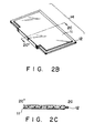
- Figs. 2A and 2B are perspective views showing the construction of a DBC plate according to one embodiment of this invention.
- Fig. 2A shows the surface (front surface) of the plate on which a semiconductor pellet is disposed and
- Fig. 2B shows the surface (rear surface) of the plate on which a heat sink is fixed.
- Fig. 2C is a cross sectional view taken along the line 2C-2C' of Fig. 2A.
- a Cu plate 11 on which a semiconductor pellet (not shown) is disposed is fixed on a ceramic plate 12 to continuously extend from the front surface of the plate 12 to the rear surface thereof via one side surface thereof.
- Cu plates 13 serving as electrodes of a semiconductor pellet (not shown) are disposed on both sides of the Cu plate 11 on the surface of the ceramic plate 12 on which the semiconductor pellet is disposed.
- the ceramic plate 12, Cu plates 11 and 13 are fixed together in a high-temperature oxidation atmosphere.
- a DBC plate 14 is formed.
- the Cu plate 11 is formed in a "letter-U" shape as shown in Fig. 2C, and the ceramic plate 12 is inserted into the groove defined by the "U"- shaped plate.
- the DBC plate 14 can be made simple in construction, can be easily fixed, and has a high degree of heat conduction from the front to the rear surface.
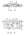
- Fig. 3 is a side view showing the construction of a power semiconductor module manufactured by use of the DBC plate 14 of the above construction.
- Fig. 3 shows the construction from which an external casing and external leads are omitted.
- a semiconductor pellet 15 is mounted on the Cu plate 11 by use of solder 16 or the like.
- the Cu plates 13 (electrodes) and electrode pads 17 on the semiconductor pellet 15 are electrically connected together via bonding wires 18 formed of aluminum.
- the DBC plate 14 on which the semiconductor pellet 15 is mounted is fixed on a heat sink 19.
- the Cu plate 11 is formed to continuously extend from the front surface of the insulative ceramic plate 12 to the rear surface thereof, the heat sink 19 and the DBC plate 14 can be electrically connected to each other by normal bonding using the solder 16 or the like.
- the semiconductor pellet 15 is a bipolar transistor
- the heat sink 19 and the Cu plate 11 connected to the collector of the transistor are electrically connected to each other. Therefore, the terminal metal member 6 becomes unnecessary.
Landscapes
- Cooling Or The Like Of Semiconductors Or Solid State Devices (AREA)
Applications Claiming Priority (2)
| Application Number | Priority Date | Filing Date | Title |
|---|---|---|---|
| JP196330/90 | 1990-07-26 | ||
| JP2196330A JP2504610B2 (ja) | 1990-07-26 | 1990-07-26 | 電力用半導体装置 |
Publications (2)
| Publication Number | Publication Date |
|---|---|
| EP0468475A1 true EP0468475A1 (de) | 1992-01-29 |
| EP0468475B1 EP0468475B1 (de) | 1996-11-27 |
Family
ID=16356033
Family Applications (1)
| Application Number | Title | Priority Date | Filing Date |
|---|---|---|---|
| EP91112419A Expired - Lifetime EP0468475B1 (de) | 1990-07-26 | 1991-07-24 | Leistungshalbleiteranordnung, geeignet zur Automation der Herstellung |
Country Status (5)
| Country | Link |
|---|---|
| US (1) | US5216279A (de) |
| EP (1) | EP0468475B1 (de) |
| JP (1) | JP2504610B2 (de) |
| KR (1) | KR950000203B1 (de) |
| DE (1) | DE69123298T2 (de) |
Cited By (7)
| Publication number | Priority date | Publication date | Assignee | Title |
|---|---|---|---|---|
| DE4300516A1 (de) * | 1993-01-12 | 1994-07-14 | Abb Ixys Semiconductor Gmbh | Leistungshalbleitermodul |
| EP0618619A1 (de) * | 1993-03-29 | 1994-10-05 | Delco Electronics Corporation | Sehr dicke Dickschicht zur Kontrolle der thermischen und stromführenden Eigenschaften von Hybridschaltungen |
| EP0746022A1 (de) * | 1995-05-30 | 1996-12-04 | Motorola, Inc. | Hybrid-Multichip-Modul und Verfahren zur seiner Herstellung |
| EP0681330A3 (de) * | 1994-05-02 | 1997-05-28 | Motorola Inc | Elektronisches Modul mit Kühlung für Halbleiter und seine Herstellung. |
| EP0706221A3 (de) * | 1994-10-07 | 1997-11-05 | Hitachi, Ltd. | Halbleiteranordnung mit einer Mehrzahl von Halbleiterelementen |
| EP0805492B1 (de) * | 1996-04-03 | 2004-06-30 | Jürgen Dr.-Ing. Schulz-Harder | Gewölbtes Metall-Keramik-Substrat |
| EP2302688A1 (de) | 2009-09-23 | 2011-03-30 | Robert Bosch GmbH | Verfahren zur Herstellung eines Substrats mit einer farbigen Interferenzfilterschicht, dieses Substrat, enthaltend eine farbige Interferenzfilterschicht, die Verwendung dieses Substrats als farbige Solarzelle oder als farbiges Solarmodul oder als Bestandteil hiervon sowie ein Array, umfassend mindestens zwei dieser Substrate |
Families Citing this family (15)
| Publication number | Priority date | Publication date | Assignee | Title |
|---|---|---|---|---|
| US5616421A (en) * | 1991-04-08 | 1997-04-01 | Aluminum Company Of America | Metal matrix composites containing electrical insulators |
| JP2839795B2 (ja) * | 1991-08-09 | 1998-12-16 | シャープ株式会社 | 半導体装置 |
| US5309014A (en) * | 1992-04-02 | 1994-05-03 | Motorola Inc. | Transistor package |
| US5480727A (en) * | 1994-02-03 | 1996-01-02 | Motorola, Inc. | Electronic device assembly and method for making |
| US5876859A (en) * | 1994-11-10 | 1999-03-02 | Vlt Corporation | Direct metal bonding |
| US5906310A (en) * | 1994-11-10 | 1999-05-25 | Vlt Corporation | Packaging electrical circuits |
| US5945130A (en) * | 1994-11-15 | 1999-08-31 | Vlt Corporation | Apparatus for circuit encapsulation |
| JP2732823B2 (ja) * | 1995-02-02 | 1998-03-30 | ヴィエルティー コーポレーション | はんだ付け方法 |
| US5798566A (en) * | 1996-01-11 | 1998-08-25 | Ngk Spark Plug Co., Ltd. | Ceramic IC package base and ceramic cover |
| US6316737B1 (en) | 1999-09-09 | 2001-11-13 | Vlt Corporation | Making a connection between a component and a circuit board |
| US6777784B1 (en) * | 2000-10-17 | 2004-08-17 | National Semiconductor Corporation | Bipolar transistor-based electrostatic discharge (ESD) protection structure with a heat sink |
| US6985341B2 (en) * | 2001-04-24 | 2006-01-10 | Vlt, Inc. | Components having actively controlled circuit elements |
| US7443229B1 (en) | 2001-04-24 | 2008-10-28 | Picor Corporation | Active filtering |
| JP4806803B2 (ja) * | 2003-10-21 | 2011-11-02 | Dowaメタルテック株式会社 | 金属−セラミックス接合基板およびその製造方法 |
| JP2013069782A (ja) | 2011-09-21 | 2013-04-18 | Toshiba Corp | 半導体装置 |
Citations (5)
| Publication number | Priority date | Publication date | Assignee | Title |
|---|---|---|---|---|
| EP0144866A2 (de) * | 1983-11-25 | 1985-06-19 | Kabushiki Kaisha Toshiba | Halbleiteranordnung mit einem Substrat |
| EP0153618A2 (de) * | 1984-02-24 | 1985-09-04 | Kabushiki Kaisha Toshiba | Verfahren zur Herstellung eines hochwärmeleitenden Substrates und Kupferleiterblech verwendbar in diesem Verfahren |
| EP0170022A2 (de) * | 1984-07-31 | 1986-02-05 | International Business Machines Corporation | Packung einer Leistungshalbleiteranordnung für die Montage auf einer Oberfläche |
| EP0181975A1 (de) * | 1984-11-15 | 1986-05-28 | Fuji Electric Co., Ltd. | Halbleiteranordnung mit einem Trägerkörper |
| DE3922485C1 (de) * | 1989-07-08 | 1990-06-13 | Doduco Gmbh + Co Dr. Eugen Duerrwaechter, 7530 Pforzheim, De |
Family Cites Families (5)
| Publication number | Priority date | Publication date | Assignee | Title |
|---|---|---|---|---|
| US3994430A (en) * | 1975-07-30 | 1976-11-30 | General Electric Company | Direct bonding of metals to ceramics and metals |
| US4518982A (en) * | 1981-02-27 | 1985-05-21 | Motorola, Inc. | High current package with multi-level leads |
| IT1202657B (it) * | 1987-03-09 | 1989-02-09 | Sgs Microelettronica Spa | Procedimento di fabbricazione di un dispositivo modulare di potenza a semiconduttore e dispositivo con esso ottenento |
| US5012324A (en) * | 1987-07-03 | 1991-04-30 | Doduco Gmbh And Co. Dr. Eugen Durrwachter | Flat body, particularly for use as a heat sink for electronic power components |
| DE3813364A1 (de) * | 1988-04-21 | 1989-11-02 | Bodenseewerk Geraetetech | Vorrichtung zur waermeabfuhr von bauelementen auf einer leiterplatte |
-
1990
- 1990-07-26 JP JP2196330A patent/JP2504610B2/ja not_active Expired - Lifetime
-
1991
- 1991-07-24 DE DE69123298T patent/DE69123298T2/de not_active Expired - Lifetime
- 1991-07-24 EP EP91112419A patent/EP0468475B1/de not_active Expired - Lifetime
- 1991-07-25 KR KR1019910012787A patent/KR950000203B1/ko not_active Expired - Lifetime
- 1991-07-26 US US07/736,230 patent/US5216279A/en not_active Expired - Lifetime
Patent Citations (5)
| Publication number | Priority date | Publication date | Assignee | Title |
|---|---|---|---|---|
| EP0144866A2 (de) * | 1983-11-25 | 1985-06-19 | Kabushiki Kaisha Toshiba | Halbleiteranordnung mit einem Substrat |
| EP0153618A2 (de) * | 1984-02-24 | 1985-09-04 | Kabushiki Kaisha Toshiba | Verfahren zur Herstellung eines hochwärmeleitenden Substrates und Kupferleiterblech verwendbar in diesem Verfahren |
| EP0170022A2 (de) * | 1984-07-31 | 1986-02-05 | International Business Machines Corporation | Packung einer Leistungshalbleiteranordnung für die Montage auf einer Oberfläche |
| EP0181975A1 (de) * | 1984-11-15 | 1986-05-28 | Fuji Electric Co., Ltd. | Halbleiteranordnung mit einem Trägerkörper |
| DE3922485C1 (de) * | 1989-07-08 | 1990-06-13 | Doduco Gmbh + Co Dr. Eugen Duerrwaechter, 7530 Pforzheim, De |
Cited By (11)
| Publication number | Priority date | Publication date | Assignee | Title |
|---|---|---|---|---|
| DE4300516A1 (de) * | 1993-01-12 | 1994-07-14 | Abb Ixys Semiconductor Gmbh | Leistungshalbleitermodul |
| DE4300516C2 (de) * | 1993-01-12 | 2001-05-17 | Ixys Semiconductor Gmbh | Leistungshalbleitermodul |
| EP0618619A1 (de) * | 1993-03-29 | 1994-10-05 | Delco Electronics Corporation | Sehr dicke Dickschicht zur Kontrolle der thermischen und stromführenden Eigenschaften von Hybridschaltungen |
| EP0681330A3 (de) * | 1994-05-02 | 1997-05-28 | Motorola Inc | Elektronisches Modul mit Kühlung für Halbleiter und seine Herstellung. |
| EP0706221A3 (de) * | 1994-10-07 | 1997-11-05 | Hitachi, Ltd. | Halbleiteranordnung mit einer Mehrzahl von Halbleiterelementen |
| EP0746022A1 (de) * | 1995-05-30 | 1996-12-04 | Motorola, Inc. | Hybrid-Multichip-Modul und Verfahren zur seiner Herstellung |
| US5751552A (en) * | 1995-05-30 | 1998-05-12 | Motorola, Inc. | Semiconductor device balancing thermal expansion coefficient mismatch |
| EP0805492B1 (de) * | 1996-04-03 | 2004-06-30 | Jürgen Dr.-Ing. Schulz-Harder | Gewölbtes Metall-Keramik-Substrat |
| EP2302688A1 (de) | 2009-09-23 | 2011-03-30 | Robert Bosch GmbH | Verfahren zur Herstellung eines Substrats mit einer farbigen Interferenzfilterschicht, dieses Substrat, enthaltend eine farbige Interferenzfilterschicht, die Verwendung dieses Substrats als farbige Solarzelle oder als farbiges Solarmodul oder als Bestandteil hiervon sowie ein Array, umfassend mindestens zwei dieser Substrate |
| WO2011036209A1 (de) | 2009-09-23 | 2011-03-31 | Robert Bosch Gmbh | Verfahren zur herstellung eines substrats mit einer farbigen interferenzfilterschicht, dieses substrat, enthaltend eine farbige interferenzfilterschicht, die verwendung dieses substrats als farbige solarzelle oder als farbiges solarmodul oder als bestandteil hiervon sowie ein array, umfassend mindestens zwei dieser substrate |
| US9312413B2 (en) | 2009-09-23 | 2016-04-12 | Robert Bosch Gmbh | Method for producing a substrate having a colored interference filter layer, this substrate containing a colored interference filter layer, the use of this substrate as a colored solar cell or as a colored solar module or as a component thereof, as well as an array including at least two of these substrates |
Also Published As
| Publication number | Publication date |
|---|---|
| JP2504610B2 (ja) | 1996-06-05 |
| JPH0483367A (ja) | 1992-03-17 |
| US5216279A (en) | 1993-06-01 |
| KR950000203B1 (ko) | 1995-01-11 |
| DE69123298D1 (de) | 1997-01-09 |
| DE69123298T2 (de) | 1997-04-24 |
| EP0468475B1 (de) | 1996-11-27 |
| KR920003485A (ko) | 1992-02-29 |
Similar Documents
| Publication | Publication Date | Title |
|---|---|---|
| US5216279A (en) | Power semiconductor device suitable for automation of production | |
| US6133632A (en) | Commonly housed diverse semiconductor die | |
| US6249041B1 (en) | IC chip package with directly connected leads | |
| CN100394602C (zh) | 电子线路装置及其制造方法 | |
| US7919854B2 (en) | Semiconductor module with two cooling surfaces and method | |
| US8004070B1 (en) | Wire-free chip module and method | |
| JP4217742B2 (ja) | 電動モータならびにこのような電動モータを製作するための方法 | |
| US5841183A (en) | Chip resistor having insulating body with a continuous resistance layer and semiconductor device | |
| JP2779620B2 (ja) | 半導体装置の保持器および集積回路をプラスチック・パッケージの内部に収納する方法 | |
| US5324890A (en) | Direct bond copper-output footprint | |
| EP0116289A2 (de) | Leistungshalbleitermodul und Packung | |
| JP3156630B2 (ja) | パワー回路実装ユニット | |
| US6575765B2 (en) | Interconnect assembly for an electronic assembly and assembly method therefor | |
| JPH05129505A (ja) | 電子回路素子搭載用リードフレーム | |
| JPH098224A (ja) | 半導体モジュールと電力変換装置 | |
| JPH0278265A (ja) | リードフレームおよびそのリードフレームを使用した複合半導体装置 | |
| JPH0617317Y2 (ja) | 混成集積回路の接続構造 | |
| JPH0817960A (ja) | Qfp構造半導体装置 | |
| JPS63141355A (ja) | 高出力混成集積回路組立方法 | |
| JP2771575B2 (ja) | 混成集積回路 | |
| JPS5915386B2 (ja) | 半導体装置用ヘッダの製造方法 | |
| JPS5823469A (ja) | 複合パワ−トランジスタ | |
| JPH0451488Y2 (de) | ||
| JPS60202958A (ja) | 混成集積回路装置 | |
| JPH09283887A (ja) | 半導体装置及びこの装置に用いる金属絶縁基板 |
Legal Events
| Date | Code | Title | Description |
|---|---|---|---|
| PUAI | Public reference made under article 153(3) epc to a published international application that has entered the european phase |
Free format text: ORIGINAL CODE: 0009012 |
|
| 17P | Request for examination filed |
Effective date: 19910724 |
|
| AK | Designated contracting states |
Kind code of ref document: A1 Designated state(s): DE FR GB |
|
| 17Q | First examination report despatched |
Effective date: 19940630 |
|
| GRAG | Despatch of communication of intention to grant |
Free format text: ORIGINAL CODE: EPIDOS AGRA |
|
| GRAH | Despatch of communication of intention to grant a patent |
Free format text: ORIGINAL CODE: EPIDOS IGRA |
|
| GRAH | Despatch of communication of intention to grant a patent |
Free format text: ORIGINAL CODE: EPIDOS IGRA |
|
| GRAA | (expected) grant |
Free format text: ORIGINAL CODE: 0009210 |
|
| AK | Designated contracting states |
Kind code of ref document: B1 Designated state(s): DE FR GB |
|
| REF | Corresponds to: |
Ref document number: 69123298 Country of ref document: DE Date of ref document: 19970109 |
|
| ET | Fr: translation filed | ||
| PGFP | Annual fee paid to national office [announced via postgrant information from national office to epo] |
Ref country code: FR Payment date: 19970709 Year of fee payment: 7 |
|
| PGFP | Annual fee paid to national office [announced via postgrant information from national office to epo] |
Ref country code: GB Payment date: 19970715 Year of fee payment: 7 |
|
| PLBE | No opposition filed within time limit |
Free format text: ORIGINAL CODE: 0009261 |
|
| STAA | Information on the status of an ep patent application or granted ep patent |
Free format text: STATUS: NO OPPOSITION FILED WITHIN TIME LIMIT |
|
| 26N | No opposition filed | ||
| PG25 | Lapsed in a contracting state [announced via postgrant information from national office to epo] |
Ref country code: GB Free format text: LAPSE BECAUSE OF NON-PAYMENT OF DUE FEES Effective date: 19980724 |
|
| GBPC | Gb: european patent ceased through non-payment of renewal fee |
Effective date: 19980724 |
|
| PG25 | Lapsed in a contracting state [announced via postgrant information from national office to epo] |
Ref country code: FR Free format text: LAPSE BECAUSE OF NON-PAYMENT OF DUE FEES Effective date: 19990331 |
|
| REG | Reference to a national code |
Ref country code: FR Ref legal event code: ST |
|
| PGFP | Annual fee paid to national office [announced via postgrant information from national office to epo] |
Ref country code: DE Payment date: 20100721 Year of fee payment: 20 |
|
| REG | Reference to a national code |
Ref country code: DE Ref legal event code: R071 Ref document number: 69123298 Country of ref document: DE |
|
| REG | Reference to a national code |
Ref country code: DE Ref legal event code: R071 Ref document number: 69123298 Country of ref document: DE |
|
| PG25 | Lapsed in a contracting state [announced via postgrant information from national office to epo] |
Ref country code: DE Free format text: LAPSE BECAUSE OF EXPIRATION OF PROTECTION Effective date: 20110725 |