EP0468479B1 - Rahmensynchronisierungseinrichtung mit einem seriell-zu-parallel-Umsetzer - Google Patents
Rahmensynchronisierungseinrichtung mit einem seriell-zu-parallel-Umsetzer Download PDFInfo
- Publication number
- EP0468479B1 EP0468479B1 EP91112423A EP91112423A EP0468479B1 EP 0468479 B1 EP0468479 B1 EP 0468479B1 EP 91112423 A EP91112423 A EP 91112423A EP 91112423 A EP91112423 A EP 91112423A EP 0468479 B1 EP0468479 B1 EP 0468479B1
- Authority
- EP
- European Patent Office
- Prior art keywords
- concurrency
- concurrent
- pattern
- frame
- frame synchronization
- Prior art date
- Legal status (The legal status is an assumption and is not a legal conclusion. Google has not performed a legal analysis and makes no representation as to the accuracy of the status listed.)
- Expired - Lifetime
Links
- 238000001514 detection method Methods 0.000 claims description 84
- 238000004519 manufacturing process Methods 0.000 claims description 19
- 230000002401 inhibitory effect Effects 0.000 claims description 15
- 230000003111 delayed effect Effects 0.000 description 13
- 238000010586 diagram Methods 0.000 description 5
- 238000006243 chemical reaction Methods 0.000 description 1
- ZMRUPTIKESYGQW-UHFFFAOYSA-N propranolol hydrochloride Chemical compound [H+].[Cl-].C1=CC=C2C(OCC(O)CNC(C)C)=CC=CC2=C1 ZMRUPTIKESYGQW-UHFFFAOYSA-N 0.000 description 1
- 238000007493 shaping process Methods 0.000 description 1
Images




Classifications
-
- H—ELECTRICITY
- H04—ELECTRIC COMMUNICATION TECHNIQUE
- H04J—MULTIPLEX COMMUNICATION
- H04J3/00—Time-division multiplex systems
- H04J3/02—Details
- H04J3/06—Synchronising arrangements
- H04J3/0602—Systems characterised by the synchronising information used
- H04J3/0605—Special codes used as synchronising signal
- H04J3/0608—Detectors therefor, e.g. correlators, state machines
Definitions
- This invention relates to a frame synchronization circuit for use in a receiver of a digital communication system, which is typically a PCM communication system.
- a transmitter of a digital communication system digital information signals are multiplexed into a multiplexed signal either on a word basis or on a frame basis.
- a frame synchronization pattern is inserted in the multiplexed signal at a frame period to have a predetermined pattern which does not appear in other parts of the multiplexed signal.
- the frame synchronization pattern is detected in order to get a correct understanding of a sequential order in which the digital information signals are multiplexed.
- a frame synchronization circuit is for putting operation of a timing pulse generator in correct synchronism with the frame synchronization pattern.
- a conventional frame synchronization circuit comprises a pattern detecting section for detecting a frame synchronization pattern in an input code sequence supplied to the pattern detecting section. Only when the frame synchronization pattern is detected, the pattern detecting section produces a pattern detection signal or pulse. Supplied with circuit input clock pulses as gate input clock pulses, a gating section allows passage of the gate input clock pulses so as to produce gate output clock pulses and inhibits passage of the gate input clock pulses so as not to produce the gate output clock pulses when controlled by first and second control signals, respectively. In compliance with the gate output clock pulses, a frame pulse generating section generates a frame pulse in each frame period. Supplied with the pattern detection signal and the frame pulse, a concurrency detecting section detects concurrency of the frame pulse with the pattern detection signal and produces the first and the second control signals when the frame pulse is and is not concurrent with the pattern detection signal, respectively.
- the frame pulse generating section comprises a timing pulse generator and a frame pulse generator.
- Each gate output clock pulse is used in stepping the timing pulse generator one step. Stepped in this manner, the timing pulse generator generates various timing pulses. Based on the timing pulses, the frame pulse generator generates the frame pulse. Primarily, the timing pulses are for use in other parts of the receiver.
- the frame pulse is generated at a time instant which depends on initial conditions of the timing pulse generator and the frame pulse generator. As a result, generation of the frame pulse is not necessarily concurrent with production of the pattern detection signal.
- the concurrency detecting section and the gating section are therefore used in adjusting the time instant of generation of the frame pulse by using the frame synchronization pattern so that the receiver may be operable in correct synchronism with the frame synchronization pattern.
- the pattern detection signal is used in generating the frame pulse through a loop comprising the concurrency detecting section, the gating section, the timing pulse generator, and the frame pulse generator.
- the loop has a loop delay, which must be shorter than one clock period of the circuit input clock pulses in order that the frame synchronization circuit is correctly operable and that the receiver is consequently correctly operable.
- the circuit input clock pulses have a high clock frequency, it becomes impossible to keep the loop delay shorter than one clock period.
- the conventional frame synchronization circuit has therefore been inoperable depending on the circumstances.
- a frame synchronization circuit is for adjusting generation of a frame pulse by using a frame synchronization pattern included in an input code sequence and includes pattern detecting means for detecting the frame synchronization pattern in the input code sequence to produce a pattern detection signal only when the frame synchronization pattern is detected, gating means for allowing passage of gate input clock pulses as gate output clock pulses and inhibiting the passage when supplied with first and second control signals, respectively, frame pulse generating means for generating the frame pulse in compliance with the gate output clock pulses, and concurrency detecting means for detecting concurrency of the frame pulse with the pattern detection signal to produce the first and the second control signals when the concurrency is and is not detected, respectively.
- the pattern detecting means of the above-understood frame synchronization circuit comprises: (A) a series-to-parallel converter for converting the input code sequence to first through N-th code sequences with the frame synchronization pattern converted to first through N-th synchronization patterns in the first through the N-th code sequences, where N represents a predetermined integer, the series-to-parallel converter being for frequency dividing circuit input clock pulses by N into the gate input clock pulses; and (B) a pattern detecting circuit for producing first through N-th detection signals collectively as the pattern detection signal only when the first through the N-th synchronization patterns are detected, respectively.
- the concurrency detecting means is for producing the first and the second control signals when the frame pulse is and is not concurrent with each of the first through the N-th detection signals. Furthermore, the concurrency detecting means is for producing first through N-th concurrent results when the frame pulse is concurrent with the first through the N-th detection signals.
- the above-understood frame synchronization circuit comprises a switching circuit for switching a sequential order of the first through the N-th code sequences in accordance with the first through the N-th concurrent results into first through N-th output code sequences.
- the above-described concurrency detecting means is for additionally producing first through N-th nonconcurrent results when the first through the N-th detection signals are not concurrent with the frame pulse.
- the first control signal starts from build up of one of the first through the N-th concurrent results that is earliest produced as an earliest concurrent result.
- the second control signal starts from simultaneous production of the first through the N-th nonconcurrent results due to collapse of frame synchronism.
- a conventional frame synchronization circuit will be described in order to facilitate an understanding of the present invention.
- the conventional frame synchronization circuit is an improved one revealed in the US-A-3699261 referred to hereinabove.
- Such a frame synchronization circuit is for use in a receiver of a digital communication system, which is typically a PCM communication system.
- the frame synchronization circuit has a data input terminal 11 supplied with an input code sequence, a clock input terminal 12 supplied with circuit input clock pulses a, and a plurality of timing pulse output terminals which are collectively indicated at 13 and are usually from several up to a few scores in number.
- a pattern detector 16 is for detecting a frame synchronization pattern in the input code sequence to produce a pattern detection signal or pulse b only when the frame synchronization pattern is detected.
- a clock inhibiting gate 17 is supplied with the circuit input clock pulses as gate input clock pulses and is controlled by a gate control signal which will presently be described. Controlled by the gate control signal, the clock inhibiting gate 17 allows passage of the gate input clock pulses so as to produce gate output clock pulses and inhibits passage of the gate input clock pulses so as not to produce the gate output clock pulses.
- a timing pulse generator 18 Based on the gate output clock pulses, a timing pulse generator 18 generates various receiver timing pulses and delivers them to the timing pulse output terminals 13.
- the receiver timing pulses are used in other parts of the receiver in the manner known in the art.
- the receiver timing pulses are furthermore used to make a frame pulse generator 19 generate a frame pulse c in each frame period. In the manner described heretobefore, the frame pulse is generated at a time instant which depends on initial conditions of the timing pulse generator 18 and the frame pulse generator 19.
- a concurrency delay circuit 21 produces a concurrency delay circuit output signal with a first binary level.
- the delay circuit output signal is given a second binary level with the concurrency delay.
- the first and the second binary levels are typically high and low binary levels.
- the delay circuit output signal of the high binary level will be called a delayed detection signal.
- a concurrency inhibiting gate 22 is supplied with the pattern detection signal b as an inhibit input and with the frame pulse c.
- the inhibiting gate 22 produces a concurrency gate output signal d with the high binary level. Otherwise, the gate output signal has the low binary level. It is therefore possible to understand that the gate output signal is given the high binary level when production of the pattern detection signal b is not concurrent with generation of the frame pulse c.
- the delayed detection signal is delivered to a reset input terminal R of a gate flip-flop circuit 23 as a reset input signal.
- the concurrency gate output signal d of the high binary level is delivered to a set input terminal S of the flip-flop circuit 23 as a set input signal.
- the flip-flop circuit 23 is therefore left reset from supply of the reset input signal until supply of the set input signal to produce an output signal e at an output terminal Q with a low level and is kept set from supply of the set input signal until supply of the reset input signal to produce the output signal e with a high level.
- the output signal e of the low and the high levels will be called first and second output signals.
- a gate delay circuit 24 supplies the clock inhibiting gate 17 with a delayed signal f as an inhibit input with a gate delay which will later be described.
- the delayed signal f is the gate control signal described before.
- the delayed signal f has a low and a high logic level and will be called first and second delayed signals.
- the clock inhibiting gate 17 is therefore released by the first delayed signal to allow passage of the gate input clock pulses as the gate output clock pulses and is inbibited by the second delayed signal to inhibit the passage.
- the delayed detection signal is alternatively referred to herein as a first control signal until build up of the concurrency gate output signal d.
- the concurrency gate output signal of the high binary level is referred to herein as a second control signal until build up of the delayed detection signal.
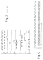
- circuit input clock pulses "a" are depicted along a first or top row. Attention will be directed to only seven circuit input clock pulses which are depicted merely for convenience of the description as first through seventh clock pulses T1 to T7. It will be surmised in the manner illustrated along a second row that the pattern detection signal b is produced in synchronism with the fifth clock pulse T5. It will furthermore be surmised as depicted along a third row that the frame pulse c is generated at the third clock pulse T3. This means that the timing pulse generator 18 generates the receiver timing pulses out of synchronism with the frame synchronization pattern and should be forcibly stepped so that the frame pulse is generated in synchronism with the frame synchronization pattern.
- the gate output signal d of the high binary level is produced with a first delay D1 in the manner illustrated along a fourth row.
- the output sinal e builds up from the first output signal to the second output signal with a second delay D2 relative to the gate output signal d.
- the second output signal is therefore produced with a sum delay (D1 + D2) relative to the frame pulse c.
- the second delay D2 is equal to a response time of the gate flip-flop circuit 23.
- the delayed detection signal makes the second output signal build down back to the first output signal.
- the second output signal has a duration comprising the circuit input clock pulses of a number which is equal to a difference between appearance of the frame synchronization pattern in the input code sequence and generation of the frame pulse, namely, two in the example being illustrated
- the clock inhibiting gate 17 inhibits the gate input clock pulses of this number to produce the gate output clock pulses in the manner depicted at g along a bottom row.
- the concurrency delay is therefore selected to be a third delay D3 which is equal to the sum delay (D1 + D2).
- the gate delay circuit 24 is merely for shaping the output signal e so that the second control signal may correctly inhibit passage of the gate input clock pulses through the clock inhibiting gate 17.
- the delayed signal f is illustrated along a fifth or punultimate row.
- the pattern detector 16 serves as a pattern detecting section for detecting the frame synchronization pattern in the input code sequence to produce the pattern detection signal b only when the frame synchronization pattern is detected.
- a combination of the gate flip-flop circuit 23, the gate delay circuit 24, and the clock inhibiting gate 17 serves as a gating section for allowing passage of the gate input clock pulses to produce the gate output clock pulses and for inhibiting passage of the gate input clock pulses so as not to produce the gate output clock pulses when controlled by the first and the second control signals, respectively.
- the gate input clock pulses are the circuit input clock pulses in the improved frame synchronization circuit.
- Another combination of the timing pulse generator 18 and the frame pulse generator 19 serves as a frame pulse generating section for generating the frame pulse c in compliance with the gate output clock pulses.
- the first control signal is produced in response to the pattern detection signal b irrespective of presence and absence of the frame pulse c. It is nevertheless possible to understand in contrast to the second control signal that the first control signal is produced when generation of the frame pulse c is concurrent with production of the pattern detection signal b. In the manner described above in connection with the concurrency gate output signal d of the high binary level, the second control signal is produced when the frame detection signal b is produced while generation of the frame pulse c is not concurrent with production of the pattern detection signal b.
- a combination of the concurrency delay circuit 21 and the concurrency inhibiting gate 22 is therefore understood as a concurrency detecting section for detecting concurrency of generation of the frame pulse c with production of the pattern detection signal b to produce the first and the second control signals when the concurrency is and is not detected, respectively.
- the improved frame synchronization circuit is operable with no theoretical restriction on a loop delay of a loop which comprises the concurrency detecting section (21, 22), the gating section, and the frame pulse generating section (18, 19). It, however, becomes difficult to manufacture the pattern detecting section (16) when the circuit input clock pulses have a high clock frequency and moreover when the frame synchronization pattern has a long pattern length.
- the frame synchronization circuit comprises similar parts designated by like reference numerals and are operable with likewise named signals.
- the pattern detecting section comprises a series-to-parallel converter 26 besides the pattern detector which is somewhat different from that described in conjunction with Fig. 1 and is referred to herein as a pattern detecting circuit and is designated again by the reference numeral 16 despite the difference.
- the series-to-parallel converter 26 Supplied with the input code sequence from the data input terminal 11 and the circuit input clock pulses "a" from the clock input terminal 12, the series-to-parallel converter 26 produces first through N-th code sequences with the frame synchronization pattern converted to first through N-th synchronization patterns in the first through the N-th code sequences, where N represents a predetermined integer which is not less than two and will be later discussed.
- the series-to-parallel converter 26 includes a frequency divider (not shown) for frequency dividing the circuit input clock pulses by the predetermined integer to produce the gate input clock pulses which will now be designated by a′. It should be noted in this connection that the gate input clock pulses are used as local timing pulses depending on the circumstances.
- the pattern detecting circuit 16 detects the first through the N-th synchronization patterns to produce first through N-th detection signals b(1) to b(N) collectively as the pattern detection signal mentioned in connection with Fig. 1. It will be assumed in the following merely for simplicity of the description that the predetermined integer N is equal to two. It will furthermore be assumed that the frame synchronization pattern has a pattern length of only two bits and consequently that an n-th synchronization pattern is composed of only one bit, where n is variable between 1 and N, both inclusive. The first through the N-th detection signals are therefore first and second pattern detection signals or pulses b(1) and b(2). In addition, the pattern detecting circuit 16 produces the first and the second code sequences as first and second output sequences including the first and the second synchronization patterns as first and second frame synchronization bits F1 and F2.
- the input code sequence includes a first part having a length of a frame period P and a second part following the first part.
- the first part will be called a preceding frame.
- the second part is in another frame period and will be called a succeeding frame.
- the preceding and the succeeding frames include a common frame synchronization pattern.
- first through sixth information bits I1 to I6 follow the frame synchronization bits F1 and F2 in each frame.
- the information bits are different in general from a frame to another frame.
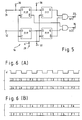
- the pattern detecting circuit 16 has a timing pulse input terminal 29, first and second data input terminals 31 and 32, first and second detection signal output terminals 33 and 34, and first through third data output terminals 36, 37, and 38.
- the pattern detecting circuit 16 comprises four flip-flop circuits connected to the first and the second data input terminals 31 and 32 and to the first through the third data output terminals 36 to 38 as shown and first and second AND gates connected to three of the flip-flop circuits and to the first and the second detection signal output terminals 33 and 34 in the manner depicted.
- the local timing pulses a′ are delivered to the timing pulse input terminal 29.
- the first and the second code sequences are delivered to the first and the second data input terminals 31 and 32.
- the first code sequence consists of the first frame synchronization bit F1 and the first, the third, and the fifth information bits I1, I3, and I5 in the manner depicted along a second or middle row.
- the second code sequence consists of the second frame synchronization bit F2 and the second, the fourth, and the sixth information bits I2, I4, and I6 as illustrated along a third or bottom row.
- the first and the second frame synchronization bits F1 and F2 appear simultaneously in the respective code sequences.
- the pattern detecting circuit 16 produces only one of the first and the second detection signals b(1) and b(2) by detecting one of two different ones of the frame synchronization bits F1 and F2, namely, either the first frame synchronization bit F1 or the second frame synchronization bit F2. This, however, depends on the predetermined pattern used as the frame synchronization pattern. It is therefore said herein that the first and the second detection signals b(1) and b(2) are produced when the first and the second frame synchronization bits F1 and F2 are detected by the respective AND gates.
- the first code sequence consists of the second frame synchronization bit F2 and the second, the fourth, and the sixth information bits I2, I4, and I6 in the manner depicted along an upper row.
- the second code sequence consists of the first frame synchronization bit F1 and the first, the third, and the fifth information bits I1, I3, and I5 as illustrated along a lower row.
- the first and the second detection signals b(1) and b(2) are produced when the second and the first frame synchronization bits F2 and F1 are detected by the respective AND gates. It will be understood that the second frame synchronization bit F2 appears in the first code sequence in synchronism with appearance of the first information bit I1 in the second code sequence.
- the pattern detecting circuit 16 does not take the first and the second synchronization bits F1 and F2 separately into consideration but detects the frame synchronization pattern by directing attention to a relative time relationship between the first and the second frame synchronization bits F1 and F2.
- the first and the second pattern detection signals b(1) and b(2) are delivered to a first input terminal IN(1) of a first concurrency detector 41(1) and to a first input terminal IN(1) of a second concurrency detector 41(2).
- the frame pulse c is delivered to a second input terminal IN(2) of each of the first and the second concurrency detectors 41 (suffixes omitted).
- the first concurrency detector 41(1) detects concurrency of generation of the frame pulse c with production of the first pattern detection signal b(1) to produce a first concurrent result at a concurrent result terminal OK and a first nonconcurrent result at a nonconcurrent result terminal NG when generation of the frame pulse is concurrent with production of the first pattern detection signal and when the first pattern detection signal is produced during generation of no frame pulse, namely, while generation of the frame pulse is not concurrent with production of the first pattern detection signal.
- the second concurrency detector 41(2) likewise detects concurrency of the frame pulse with the second pattern detection signal and similarly produces a second concurrent result at a concurrent result termnial OK and a second nonconcurrent result at a nonconcurrent result terminal NG when the frame pulse is and is not concurrent with the second pattern detection signal.
- the first concurrent result is delivered to a disable input terminal DIS of the second concurrency detector 41(2).
- the second concurrent result is delivered to a disable input terminal DIS of the first concurrency detector 41(1).
- the first and the second concurrent results are delivered to an OR gate 42 for producing an OR output signal, which is supplied to the gate flip-flop circuit 23 as the first control signal.
- the first and the second nonconcurrent results are delivered to an AND gate 43 for producing an AND output signal, which is supplied to the gate flip-flop circuit 23 as the second control signal.
- the AND output signal is furthermore delivered to an enable input terminal EN of each of the first and the second concurrency detectors 41 to enable the above-mentioned other of the concurrency detectors 41 by releasing the disabled state of the concurrency detector 41 under consideration.
- the first and the second concurrent results are supplied to a switching circuit 44 for switching a sequential order or channels of the first and the second output sequences in the manner which will later become clear.
- each of the first and the second concurrency detectors 41 has a timing pulse input terminal CLK supplied with the local timing pulses a′, the first and the second input terminals IN(1) and IN(2), the enable and the disable input terminals EN and DIS, and the concurrent and the nonconcurrent result terminals OK and NG.
- Each concurrency detector 41 comprises two inhibiting gates, an OR gate, and six flip-flop circuits which are connected together and to the input and the output terminals in the manner illustrated.
- the pattern detecting circuit 16 delivers the first pattern detection signal b(1) with a high logic level from the first AND gate to the first detection signal output terminal 33 when the first frame synchronization bit F1 is detected in the first code sequence supplied to the first data input terminal 31.
- the second AND gate delivers the second pattern detection signal b(2) with a low logic level to the second detection signal output terminal 34 even when the second frame synchronization bit F2 is detected in the second code sequence supplied to the second data input terminal 32.
- the first concurrency detector 41(1) may produce the nonconcurrent result at first, for example, during the preceding frame.
- the second concurrency detector 41(2) produces the nonconcurrent result.
- the first and the second concurrency detectors 41 are therefore kept enabled.
- generation of the frame pulse c becomes concurrent with appearance of the first and the second frame synchronization bits F1 and F2 in the first and the second code sequences and consequently with production of the first and the second pattern detection signals b(1) and b(2).
- the first concurrency detector 41(1) produces the concurrent result earlier than the second concurrency detector 41(2).
- the first concurrency detector 41(1) remains in an enabled state of capable of repeatedly producing the concurrent result in successive frame periods and disables the second concurrency detector 41(2), which is kept in the disabled state until enabled when the first concurrency detector 41(1) happens to produce the nonconcurent result due to collapse of the frame synchronism for some reason or another.
- the AND output signal becomes to have the high logic level. Stated otherwise, the first and the second concurrency detectors 41 are enabled when the first and the second nonconcurrent results are simultaneously produced.
- the first frame synchronization bit F1 appears in the second code sequence one timing pulse period earlier than appearance of the second frame synchronization bit F2 in the first code sequence.
- the pattern detecting circuit 16 delivers the second pattern detection signal b(2) with the high logic level from the second AND gate to the second detection signal output terminal 34 when the first frame synchronization bit F1 is detected in the second code sequence supplied to the second data input terminal 32.
- the first AND gate delivers the first pattern detection signal b(1) with the low logic level to the first detection signal output terminal 33 when the first frame synchronization bit F1 is detected one timing pulse period later in the first code sequence supplied to the first data input terminal 31.
- the first concurrency detector 41(1) produces the nonconcurrent result.
- the second concurrency detector 41(2) may produce the nonconcurrent result at first. In due cource, generation of the frame pulse c becomes concurrent with appearance of the first frame synchronization bit F1 in the second code sequence and consequently with production of the second pattern detection signal b(2) of the high logic level.
- the second concurrency detector 41(2) therefore produces the concurrent result earlier than the first concurrency detector 41(1).
- the second concurrency detector 41(2) remains in an enabled state of capable of repeatedly producing the concurrent result in successive frame periods and disables the first concurrency detector 41(1), which is kept in the disabled state until enabled when the second concurrency detector 41(2) happens to produce the nonconcurrent result due to collapse of frame synchronism for some reason or another.
- the first and the second concurrency detectors 41 are enabled by the AND output signal of the high logic level.
- the gate delay circuit 24 is not essential to its operation.
- the first and the second delayed signals may therefore be referred to as the first and the second output signals. It is possible in this event to understand that a combination of the gate flip-flop circuit 23 and the gate delay circuit 24 serves as a flip-flop unit for producing the first and the second output signals when reset by the first control signal and when set by the second control signal, respectively.
- the switching circuit 44 switches the sequential order of the first and the second output sequences into first and second output code sequences.
- the first and the second output sequences are produced, in the first case, as the first and the second output code sequences with the sequential order left untouched.
- the first and the second output sequences are produced as the second and the first output code sequences with the sequential order switched.
- the first and the second output code sequences are delivered to first and second data output terminals 46 and 47.
- the switching circuit 44 has a timing pulse input terminal CLK, first through third data input terminals 51, 52, and 53, first and second result input terminals 56 and 57, and the first and the second data output terminals 46 and 47.
- the first and the second output sequences are supplied from the first to the third data output terminals 36 through 38 to the first through the third data input terminals 51 to 53.
- the first and the second concurrent results are supplied from the concurrent result terminals OK's of the first and the second concurrency detectors 41 to the first and the second result input terminals 56 and 57.
- a NAND gate is connected to the first result input terminal 56 directly and to the second result input terminal 57 through an inverter to produce a selection signal SEL, which has low and high binary levels when the first and the second concurrent results are produced.
- Each of first and second selectors 58(1) and 58(2) has a selection input terminal SEL, first and second input terminals A and B, and an output terminal Y.
- the selection signal is supplied to the selection input terminals of the first and the second selectors 58 (suffixed omitted). When the selection signal has the low and the high binary levels, the selectors 58 select signals supplied to the first and the second input terminals A and B, respectively.
- the first input terminal A of the first selector 58(1) is connected to the second data input terminal 53.
- the second input terminal B of the second selector 58(2) is connected to the first data input terminal 51.
- the second input terminal B of the first selector 58(1) and the first input terminal A of the second selector 58(2) are connected in common to the third data input terminal 52.
- Each of first and second flip-flop circuits 59(1) and 59(2) has C and D input terminals and a Q output terminal.
- the C input terminals of the first and the second flip-flop circuits 59 (suffixes omitted) are connected in common to the timing pulse input terminal CLK.
- the D input terminals of the first and the second flip-flop circuits 59 are connected to the output terminals Y of the first and the second selectors 58.
- the Q output terminals of the first and the second flip-flop circuits 59 are connected to the first and the second data output terminals 46 and 47.
- the local timing pulses a′ are depicted along a first or top row in commun to Fig. 9 (B). Attention will be directed to the first case.
- the first and the second pattern detection signals b(1) and b(2) are illustrated along second and third rows.
- the first and the second concurrent results are produced with the high and the low logic levels.
- the selection signal therefore keeps the low logic level as depicted along a fourth row.
- the first and the second output code sequences are therefore delivered to the first and the second data output terminals 46 and 47 in the manner depicted along a fifth row and a sixth or bottom row.
- Fig. 9 (B) the second case is illustrated.
- the first and the second pattern detection signals b(1) and b(2) are depicted along a first or top and a second row.
- the first and the second concurrent results are produced with the low and the high logic levels.
- the selection signal therefore keeps the high logic level as depicted along a third row.
- the first and the second output code sequences are delivered to the first and the second data output terminals 46 and 47 in the manner illustrated along a fourth and a fifth or bottom row.
- a combination of the first and the second concurrency detectors 41, the OR gate 42, and the AND gate 43 serves as a concurrency detecting section.
- the concurrence detecting section (41, 42, 43) produces the first and the second nonconcurrent results when the pattern detection signals are produced nonconcurrent, namely, out of concurrency, with the frame pulse due to, for example, collapse of frame synchronism.
- One of the first and the second pattern detection signals such as the first pattern detection signal b(1) in Fig. 9 (A) or the second pattern detection signal b(2) in Fig. 9 (B), is produced earliest as an earliest detection signal in each frame period.
- one of the first and the second concurrency detectors 41 produces one of the first and the second concurrent results as an earliest concurrent result to serve as a particular concurrency detector when the earliest pattern detection signal is produced concurrent with generation of the frame pulse.
- the particular concurrency detector remains in the enabled state described above with reference to Figs. 3 and 5 through 7 and puts the other of the concurrency detectors 41 in the disabled state described before by turning back to Fig. 3.
- the concurrency detecting section produces in this manner only one of the first and the second concurrent results as the earliest concurrent result, whichever one of the first and the second concurrency detectors 41 may serve as the particular concurrency detector depending on the first and the second synchronization patterns. It may therefore be said that the concurrency detecting section is capable of producing the first and the second concurrent results, namely, is for producing the first and the second concurrent results, when generation of the frame pulse c is concurrent with production of the first and the second pattern detection signals b(1) and b(2).
- the first control signal starts from production of the earliest concurrent result and ends at simultaneous production of the first and the second nonconcurrent results.
- the second control signal starts from the simultaneous production of the first and the second nonconcurrent results and ends at later production of the earliest concurrent result.
- the predetermined integer N may be equal to three or more. It should be noted in this connection that the frame synchronization pattern of a long pattern length is desirable when rapid restoration of the frame synchronism is important. This, however, results in the pattern detector 16 of a complicated structure and in restricted clock frequency of the circuit input clock pulses used therein. Generally speaking, the pattern detector or the pattern detecting circuit 16 is operable at as high a clock frequency as about 500 MHz at present. Only about four bits have therefore been used as the pattern length of the frame synchronization pattern in a conventional frame sychronization circuit.
- the series-to-parallel converter 26 is simpler in structure than the pattern detector 16 and is operable at a higher clock frequency of about 2.5 GHz.
- Use of the predetermined integer N makes it possible to lengthen the pattern length and to use the local timing pulses having a highest possible clock frequency.
- the predetermined integer N should be less than twice the number of bits in each frame synchronization pattern and should be an integral submultiple of the number of bits in each frame period.
- the pattern detecting circuit 16 is less power consuming, more highly integrated, and lower priced when put into operation at a lower clock frequency. Selection of a greater number as the predetermined integer, however, results in a frame synchronization circuit of a larger scale. These factors should therefore be taken into consideration on actually determining the predetermined integer.
- the predetermined integer of eight and the pattern length of thirty-two bits were used in frame synchronization circuits which were actually manufactured according to this invention and were tested.
- the pattern detecting circuit 16 of Fig. 5 is operable when the frame synchronization pattern consists of the first frame synchronization bit F1 of the high binary level and the second frame synchronization bit F2 of the low binary level.
- the pattern detecting circuit 16 may comprise first through N-th shift registers and a plurality of AND gates in the manner known in the art. In any event, the pattern detecting circuit 16 should have a structure which is applicable to the predetermined pattern used as the frame synchronization pattern.
- the pattern detecting circuit 16 detects one of different ones of the first through the N-th synchronization patterns earliest in each frame period of the input code sequence to produce the above-mentioned earliest detection signal when that one of the different ones of the first through the N-th synchronization patterns is detected. It should be noted that there are first through N-th cases in connection with a combination of the first through the N-th code sequences and consequently with a combination of the first through the N-th synchronization patterns.
- the concurrency detecting section (41, 42, 43) should comprise first through N-th concurrency detectors 41 instead of only first and second concurrency detectors.
- the disable input terminal DIS of each of the first through the N-th concurrency detectors 41 should be supplied through an OR gate (not shown) with the concurrent result produced by any one of the first through the N-th concurrency detectors 41.
- the concurrency detecting section is not different in principle from that described in conjunction with Figs. 3 and 5. The fact should clearly be noted in this connection that the concurrency detecting section is excellently operable despite conversion of the input code sequence to the first through the N-th code sequences. This is because one of the first through the N-th concurrency detectors 41 disables (N - 1) remaining ones of the concurrency detectors 41 as soon as the earliest concurrent result is produced by that one of the concurrency detectors 41.
- the switching circuit 44 should switch the sequential order of first through N-th output sequences which are produced by the pattern detecting section (26, 16) together with the first through the N-th synchronization patterns. It should be noted in this connection that the first through the N-th output sequences are produced in connection with the first through the N-th cases. It is nevertheless believed that the switching circuit 44 is readily implemented when attention is directed to the fact that the first through the N-th cases are automatically discriminated from one another by the earliest concurrent result produced by the concurrency detecting section.
- the predetermined integer N is equal to three or more
- at least one of the first through the N-th synchronization patterns may consist of two or more frame synchronization bits. Even in this event, it will readily be possible to implement the pattern detecting circuit 16, the switching circuit 44, and the like.
Landscapes
- Engineering & Computer Science (AREA)
- Computer Networks & Wireless Communication (AREA)
- Signal Processing (AREA)
- Synchronisation In Digital Transmission Systems (AREA)
- Time-Division Multiplex Systems (AREA)
- Transmission Systems Not Characterized By The Medium Used For Transmission (AREA)
Claims (8)
- Rahmensynchronisierungsschaltung zum Einstellen der Erzeugung eines Rahmenimpulses (c) durch Verwenden eines in einer Eingangscodesequenz enthaltenen Rahmensynchronisierungsmusters, wobei die Rahmensynchronisierungsschaltung aufweist: eine Mustererfassungseinrichtung (16) zum Feststellen des Rahmensynchronisierungsmusters in der Eingangscodesequenz, um nur dann ein Mustererfassungssignal (b(1) - b(N)) zu erzeugen, wenn das Rahmensynchronisierungsmuster festgestellt wird, eine Torsteuerungseinrichtung (17), um Gattereingangstaktimpulse (a′) als Gatterausgangstaktimpulse durchzulassen oder den Durchgang zu blockieren, wenn der Torsteuerungseinrichtung ein erstes bzw. ein zweites Steuersignal (R, S) zugeführt wird, eine Rahmenimpulserzeugungseinrichtung (19) zum Erzeugen des Rahmenimpulses gemäß den Gatterausgangstaktimpulsen (g) und eine Gleichzeitigkeitserfassungseinrichtung (41) zum Feststellen der Gleichzeitigkeit des Rahmenimpulses (c) und des Mustererfassungssignals (b(1) - b(N)), um das erste und das zweite Steuersignal (OK, NG, R, S) zu erzeugen, wenn die Gleichzeitigkeit festgestellt bzw. nicht festgestellt wird,
wobei die Mustererfassungseinrichtung aufweist:
einen Serien-Parallel-Umsetzer (26) zum Umwandeln der Eingangscodesequenz in erste bis N-te Codesequenzen, wobei das Rahmensynchronisierungsmuster in erste bis N-te Synchronisierungsmuster in den ersten bis N-ten Codesequenzen umgewandelt wird, wobei N eine vorgegebene ganze Zahl darstellt, und wobei der SerienParallel-Umsetzer zum Frequenzteilen von Schaltungseingangstaktimpulsen (a) durch N in die Gattereingangstaktimpulse (a′) dient; und
eine Mustererfassungsschaltung (16), um nur dann erste bis N-te Erfassungssignale (b(1) - b(N)) gemeinsam als das Mustererfassungssignal zu erzeugen, wenn die ersten bis N-ten Synchronisierungsmuster jeweils festgestellt werden;
wobei die Gleichzeitigkeits erfassungseinrichtung (41) zum Erzeugen des ersten und des zweiten Steuersignals (OK, NG, R, S) dient, wenn der Rahmenimpuls (c) gleichzeitig bzw. nicht gleichzeitig mit den ersten bis N-ten Erfassungssignalen (b(1) - b(N)) erzeugt wird, und die Gleichzeitigkeitserfassungseinrichtung zum Erzeugen erster bis N-ter Gleichzeitigkeitsergebnisse (OK) dient, wenn der Rahmenimpuls (c) gleichzeitig mit den ersten bis N-ten Erfassungssignalen (b(1) - b(N) erzeugt wird;
wobei die Rahmensynchronisierungsschaltung eine Schaltschaltung (44) zum Umschalten einer sequentiellen Reihenfolge der ersten bis N-ten Codesequenzen gemäß den ersten bis N-ten Gleichzeitigkeitsergebnissen (OK) in erste bis N-te Ausgangscodesequenzen (46, 47) aufweist. - Rahmensynchronisierungsschaltung nach Anspruch 1, wobei die Gleichzeitigkeitserfassungseinrichtung zum Erzeugen erster bis N-ter Nichtgleichzeitigkeitsergebnisse dient, wenn die ersten bis N-ten Erfassungssignale nicht gleichzeitig mit dem Rahmenimpuls erzeugt werden, wobei das erste Steuersignal von einem der ersten bis N-ten Gleichzeitigkeitsergebnisse beginnt, das zuerst als ein frühestes Gleichzeitigkeitsergebnis erzeugt wird, und das zweite Steuersignal von der gleichzeitigen Erzeugung der ersten bis N-ten Nichtgleichzeitigkeitsergebnisse beginnt.
- Rahmensynchronisierungsschaltung nach Anspruch 1 oder 2, wobei
die Mustererfassungsschaltung zum Erzeugen eines frühesten der ersten bis N-ten Erfassungssignale als ein frühestes Erfassungssignal dient;
die Gleichzeitigkeitserfassungseinrichtung zum Erzeugen des frühesten Gleichzeitigkeitsergebnisses dient, wenn der Rahmenimpuls und das früheste Erfassungssignal gleichzeitig vorhanden sind;
und die Schaltschaltung zum Umschalten der sequentiellen Reihenfolge gemäß dem frühesten Gleichzeitigkeitsergebnis dient. - Rahmensynchronisierungsschaltung nach einem der Ansprüche 1 bis 3, wobei die Gleichzeitigkeitserfassungseinrichtung aufweist:
erste bis N-te Gleichzeitigkeitsdetektoren, denen der Rahmenimpuls gemeinsam sowie die ersten bis N-ten Erfassungssignale zugeführt werden, wobei jeder der Gleichzeitigkeitsdetektoren einen Freigabe-Eingangsanschluß und einen Sperreingangsanschluß sowie einen Gleichzeitigkeitsergebnis- und einen Nichtgleichzeitigkeitsergebnisanschluß aufweist, wobei der Gleichzeitigkeitsergebnisanschluß mit dem Sperreingangsanschluß mindestens eines der anderen Gleichzeitigkeitsdetektoren verbunden ist, wobei die ersten bis N-ten Gleichzeitigkeitsergebnisse an den Gleichzeitigkeitsergebnisanschlüssen der ersten bis N-ten Gleichzeitigkeitsdetektoren und die ersten bis N-ten Nichtgleichzeitigkeitsergebnisse an den Nichtgleichzeitigkeitsergebnisanschlüssen der ersten bis N-ten Gleichzeitigkeitsdetektoren erzeugt werden, wobei einem der ersten bis N-ten Gleichzeitigkeitsdetektoren das früheste Erfassungssignal zugeführt wird, so daß er als besonderer Gleichzeitigkeitsdetektor zum Erzeugen des frühesten Gleichzeitigkeitsergebnisses wirkt und in einem Freigabezustand verbleibt, in dem entweder eines der ersten bis N-ten Gleichzeitigkeitsergebnisse oder eines der ersten bis N-ten Nichtgleichzeitigkeitsergebnisse erzeugt werden kann, wobei mindestens einer der übrigen der ersten bis N-ten Gleichzeitigkeitsdetektoren durch das früheste Gleichzeitigkeitsergebnis in einen gesperrten Zustand eingestellt wird, um keines der ersten bis N-ten Gleichzeitigkeitsergebnisse und mindestens eines der ersten bis N-ten Nichtgleichzeitigkeitsergebnisse geeignet zu erzeugen;
ein mit den Gleichzeitigkeitsergebnisanschlüssen der ersten bis N-ten Gleichzeitigkeitsdetektoren verbundenes ODER-Gatter, um ein ODER-Ausgangssignal der ersten bis N-ten Gleichzeitigkeitsergebnisse als das erste Steuersignal zu erzeugen; und
ein mit den Nichtgleichzeitigkeitsergebnisanschlüssen der ersten bis N-ten Gleichzeitigkeitsdetektoren und mit den Freigabe-Eingangsanschlüssen der ersten bis N-ten Gleichzeitigkeitsdetektoren verbundenes UND-Gatter, um ein UND-Ausgangssignal der ersten bis N-ten Nichtgleichzeitigkeitsergebnisse als das zweite Steuersignal zu erzeugen, wobei das UND-Ausgangssignal dazu dient, die ersten bis N-ten Gleichzeitigkeitsdetektoren in Freigabezustände einzustellen, in denen die ersten bis N-ten Gleichzeitigkeitsergebnisse und die ersten bis N-ten Nichtgleichzeitigkeitsergebnisse erzeugt werden können. - Rahmensynchronisierungsschaltung nach Anspruch 3 oder 4, wobei die Mustererfassungseinrichtung zum Feststellen eines von verschiedenen der ersten bis N-ten Synchronisierungsmuster dient, das in jeder Rahmenperiode der Eingangscodesequenz am frühesten vorhanden ist, um das früheste Erfassungssignal zu erzeugen, wenn das eine der verschiedenen Synchronisierungsmuster festgestellt wird.
- Rahmensynchronisierungsschaltung nach einem der Ansprüche 1 bis 5, wobei das Rahmensynchronisierungsmuster eine erste vorgegebene Anzahl von Bits lang ist und die Eingangscodesequenz eine Rahmenperiode aufweist, die eine zweite vorgegebene Anzahl von Bits lang ist, wobei die vorgegebene ganze Zahl kleiner als das Zweifache der ersten vorgegebenen Anzahl und ein in der zweiten vorgegebenen Anzahl enthaltener ganzzahliger Faktor ist.
- Rahmensynchronisierungsschaltung nach Anspruch 6, wobei die vorgegebene ganze Zahl gleich Acht ist, das Rahmensynchronisierungsmuster eine Länge von 32 Bits besitzt und jeder der ersten bis achten Synchronisierungsmuster eine Länge von vier Bits besitzt.
- Rahmensynchronisierungsschaltung nach einem der Ansprüche 1 bis 7, wobei die Torsteuerungseinrichtung aufweist:
eine Flipflopeinheit zum Erzeugen eines ersten und eines zweiten Ausgangssignals, wenn die Einheit durch das erste Steuersignal zurückgesetzt bzw. durch das zweite Steuersignal gesetzt wird; und
ein Blockiergatter, das durch das erste Ausgangssignal freigegeben wird, um die Gattereingangstaktimpulse durchzulassen, um die Gatterausgangstaktimpulse zu erzeugen, und durch das zweite Ausgangssignal blockiert wird, um den Durchgang der Gattereingangstaktimpulse zu blockieren, um keine Gatterausgangstaktimpulse zu erzeugen.
Applications Claiming Priority (2)
| Application Number | Priority Date | Filing Date | Title |
|---|---|---|---|
| JP197559/90 | 1990-07-25 | ||
| JP2197559A JPH0748725B2 (ja) | 1990-07-25 | 1990-07-25 | フレーム同期回路 |
Publications (3)
| Publication Number | Publication Date |
|---|---|
| EP0468479A2 EP0468479A2 (de) | 1992-01-29 |
| EP0468479A3 EP0468479A3 (en) | 1992-07-08 |
| EP0468479B1 true EP0468479B1 (de) | 1995-10-18 |
Family
ID=16376512
Family Applications (1)
| Application Number | Title | Priority Date | Filing Date |
|---|---|---|---|
| EP91112423A Expired - Lifetime EP0468479B1 (de) | 1990-07-25 | 1991-07-24 | Rahmensynchronisierungseinrichtung mit einem seriell-zu-parallel-Umsetzer |
Country Status (5)
| Country | Link |
|---|---|
| US (1) | US5313500A (de) |
| EP (1) | EP0468479B1 (de) |
| JP (1) | JPH0748725B2 (de) |
| AU (1) | AU636993B2 (de) |
| DE (1) | DE69113905T2 (de) |
Families Citing this family (9)
| Publication number | Priority date | Publication date | Assignee | Title |
|---|---|---|---|---|
| JP2732759B2 (ja) * | 1992-07-15 | 1998-03-30 | 沖電気工業株式会社 | フレーム同期制御方式 |
| US5526297A (en) * | 1994-07-29 | 1996-06-11 | Comsat Corporation | Random unique word detection method and apparatus |
| KR0133423B1 (ko) * | 1994-12-09 | 1998-04-27 | 양승택 | 프레임 동기 장치(frame synchronizng device) |
| JP2817660B2 (ja) * | 1995-03-30 | 1998-10-30 | 日本電気株式会社 | 同期回路 |
| KR0154852B1 (ko) * | 1995-10-25 | 1998-11-16 | 김광호 | 프레임 동기신호 검출장치 |
| JP3441589B2 (ja) * | 1996-02-29 | 2003-09-02 | シャープ株式会社 | 同期検出復調回路 |
| JPH1174878A (ja) * | 1997-08-28 | 1999-03-16 | Mitsubishi Electric Corp | デジタルデータ伝送システム |
| JP2001156761A (ja) * | 1999-11-29 | 2001-06-08 | Ando Electric Co Ltd | パターン同期回路 |
| US20020184412A1 (en) * | 2001-06-02 | 2002-12-05 | Stevens James Ray | System and method for locating and aligning to framing bits |
Citations (1)
| Publication number | Priority date | Publication date | Assignee | Title |
|---|---|---|---|---|
| US3699261A (en) * | 1969-11-27 | 1972-10-17 | Nippon Electric Co | Frame synchronizing circuit for high clock frequency digital communication |
Family Cites Families (7)
| Publication number | Priority date | Publication date | Assignee | Title |
|---|---|---|---|---|
| FR2377729A1 (fr) * | 1977-01-14 | 1978-08-11 | Thomson Csf | Dispositif de decodage de signaux numeriques, et systeme comportant un tel dispositif |
| US4404542A (en) * | 1980-12-05 | 1983-09-13 | Rca Corporation | Digital sequence detector |
| DE3438369A1 (de) * | 1984-10-19 | 1986-04-24 | ANT Nachrichtentechnik GmbH, 7150 Backnang | Digitales nachrichtenuebertragungssystem |
| NZ220548A (en) * | 1986-06-18 | 1990-05-28 | Fujitsu Ltd | Tdm frame synchronising circuit |
| JPH0828691B2 (ja) * | 1988-03-14 | 1996-03-21 | 富士通株式会社 | フレーム同期方式 |
| US4879731A (en) * | 1988-08-24 | 1989-11-07 | Ampex Corporation | Apparatus and method for sync detection in digital data |
| US5058141A (en) * | 1990-03-01 | 1991-10-15 | Ag Communication Systems Corporation | Single circuit for detecting a frame synchronization pattern and generating control signals |
-
1990
- 1990-07-25 JP JP2197559A patent/JPH0748725B2/ja not_active Expired - Lifetime
-
1991
- 1991-07-24 DE DE69113905T patent/DE69113905T2/de not_active Expired - Lifetime
- 1991-07-24 EP EP91112423A patent/EP0468479B1/de not_active Expired - Lifetime
- 1991-07-25 US US07/735,732 patent/US5313500A/en not_active Expired - Lifetime
- 1991-07-25 AU AU81337/91A patent/AU636993B2/en not_active Expired
Patent Citations (1)
| Publication number | Priority date | Publication date | Assignee | Title |
|---|---|---|---|---|
| US3699261A (en) * | 1969-11-27 | 1972-10-17 | Nippon Electric Co | Frame synchronizing circuit for high clock frequency digital communication |
Non-Patent Citations (1)
| Title |
|---|
| Patent Abstracts of Japan vol. 14, no. 557 (E-1011) 11 December 1990; & JP-A-02 239735 (FUJITSU LTD.) 21 September 1990 * |
Also Published As
| Publication number | Publication date |
|---|---|
| JPH0748725B2 (ja) | 1995-05-24 |
| EP0468479A3 (en) | 1992-07-08 |
| US5313500A (en) | 1994-05-17 |
| AU636993B2 (en) | 1993-05-13 |
| DE69113905T2 (de) | 1996-04-25 |
| EP0468479A2 (de) | 1992-01-29 |
| DE69113905D1 (de) | 1995-11-23 |
| JPH0483435A (ja) | 1992-03-17 |
| AU8133791A (en) | 1992-01-30 |
Similar Documents
| Publication | Publication Date | Title |
|---|---|---|
| JP2747077B2 (ja) | フレーム同期回路 | |
| CA1298420C (en) | Demultiplexer system | |
| US4151373A (en) | Data transmission system | |
| US3069504A (en) | Multiplex pulse code modulation system | |
| EP0468479B1 (de) | Rahmensynchronisierungseinrichtung mit einem seriell-zu-parallel-Umsetzer | |
| EP0456258B1 (de) | Netzsynchronisierungseinheit für eine Vermittlungsanlage | |
| EP0131233B1 (de) | Programmierbarer Taktgenerator hoher Geschwindigkeit | |
| US5012198A (en) | Digital PLL circuit having reduced lead-in time | |
| US4053715A (en) | Stuffing channel unit for telephone pcm system | |
| US3825683A (en) | Line variation compensation system for synchronized pcm digital switching | |
| EP0268409B1 (de) | Multiplexer für Taktsignale | |
| US3603735A (en) | Synchronizing arrangement for a pulse-communication receiver | |
| SU1181567A3 (ru) | Устройство фазировани числовых последовательностей | |
| CA1120120A (en) | Frame search control for digital transmission system | |
| US4955040A (en) | Method and apparatus for generating a correction signal in a digital clock recovery device | |
| US3719890A (en) | Transceiver for peripheral station of multiplex telecommunication system | |
| EP0409168B1 (de) | Schaltung zur elastischen Speicherung | |
| CA1287150C (en) | Synchronisation arrangements for a digital telecommunications exchange system | |
| US3087996A (en) | Hisashi kaneko | |
| US5270713A (en) | Decode circuit capable of decreasing the amount of hardware required by selectively using one of a plurality of clock signals | |
| KR100363411B1 (ko) | 그룹간선상의 채널선택 로직회로 | |
| SU1688415A1 (ru) | Устройство дл мажоритарного декодировани в целом | |
| JP2876747B2 (ja) | フレーム同期回路 | |
| JP2617575B2 (ja) | データ速度変換回路 | |
| GB1582125A (en) | Telecommunication systems |
Legal Events
| Date | Code | Title | Description |
|---|---|---|---|
| PUAI | Public reference made under article 153(3) epc to a published international application that has entered the european phase |
Free format text: ORIGINAL CODE: 0009012 |
|
| 17P | Request for examination filed |
Effective date: 19910821 |
|
| AK | Designated contracting states |
Kind code of ref document: A2 Designated state(s): DE FR GB |
|
| PUAL | Search report despatched |
Free format text: ORIGINAL CODE: 0009013 |
|
| AK | Designated contracting states |
Kind code of ref document: A3 Designated state(s): DE FR GB |
|
| 17Q | First examination report despatched |
Effective date: 19940218 |
|
| GRAA | (expected) grant |
Free format text: ORIGINAL CODE: 0009210 |
|
| AK | Designated contracting states |
Kind code of ref document: B1 Designated state(s): DE FR GB |
|
| REF | Corresponds to: |
Ref document number: 69113905 Country of ref document: DE Date of ref document: 19951123 |
|
| ET | Fr: translation filed | ||
| PLBE | No opposition filed within time limit |
Free format text: ORIGINAL CODE: 0009261 |
|
| STAA | Information on the status of an ep patent application or granted ep patent |
Free format text: STATUS: NO OPPOSITION FILED WITHIN TIME LIMIT |
|
| 26N | No opposition filed | ||
| REG | Reference to a national code |
Ref country code: GB Ref legal event code: IF02 |
|
| PGFP | Annual fee paid to national office [announced via postgrant information from national office to epo] |
Ref country code: DE Payment date: 20100721 Year of fee payment: 20 Ref country code: FR Payment date: 20100805 Year of fee payment: 20 |
|
| PGFP | Annual fee paid to national office [announced via postgrant information from national office to epo] |
Ref country code: GB Payment date: 20100721 Year of fee payment: 20 |
|
| REG | Reference to a national code |
Ref country code: DE Ref legal event code: R071 Ref document number: 69113905 Country of ref document: DE |
|
| REG | Reference to a national code |
Ref country code: DE Ref legal event code: R071 Ref document number: 69113905 Country of ref document: DE |
|
| REG | Reference to a national code |
Ref country code: GB Ref legal event code: PE20 Expiry date: 20110723 |
|
| PG25 | Lapsed in a contracting state [announced via postgrant information from national office to epo] |
Ref country code: GB Free format text: LAPSE BECAUSE OF EXPIRATION OF PROTECTION Effective date: 20110723 |
|
| PG25 | Lapsed in a contracting state [announced via postgrant information from national office to epo] |
Ref country code: DE Free format text: LAPSE BECAUSE OF EXPIRATION OF PROTECTION Effective date: 20110725 |