EP0468583B1 - Circuit excitateur - Google Patents
Circuit excitateur Download PDFInfo
- Publication number
- EP0468583B1 EP0468583B1 EP91201893A EP91201893A EP0468583B1 EP 0468583 B1 EP0468583 B1 EP 0468583B1 EP 91201893 A EP91201893 A EP 91201893A EP 91201893 A EP91201893 A EP 91201893A EP 0468583 B1 EP0468583 B1 EP 0468583B1
- Authority
- EP
- European Patent Office
- Prior art keywords
- bus line
- voltage
- circuit module
- output
- terminal
- Prior art date
- Legal status (The legal status is an assumption and is not a legal conclusion. Google has not performed a legal analysis and makes no representation as to the accuracy of the status listed.)
- Expired - Lifetime
Links
- 238000003780 insertion Methods 0.000 claims description 21
- 230000037431 insertion Effects 0.000 claims description 21
- 230000013011 mating Effects 0.000 description 5
- 230000003068 static effect Effects 0.000 description 5
- 230000007704 transition Effects 0.000 description 5
- 239000013256 coordination polymer Substances 0.000 description 4
- 230000001052 transient effect Effects 0.000 description 4
- 230000005540 biological transmission Effects 0.000 description 3
- 238000012546 transfer Methods 0.000 description 3
- 230000008901 benefit Effects 0.000 description 2
- 238000004891 communication Methods 0.000 description 2
- 230000007423 decrease Effects 0.000 description 2
- 230000000694 effects Effects 0.000 description 2
- 238000005516 engineering process Methods 0.000 description 2
- 230000003071 parasitic effect Effects 0.000 description 2
- 238000012545 processing Methods 0.000 description 2
- 230000009471 action Effects 0.000 description 1
- 230000004888 barrier function Effects 0.000 description 1
- 230000000295 complement effect Effects 0.000 description 1
- 230000008878 coupling Effects 0.000 description 1
- 238000010168 coupling process Methods 0.000 description 1
- 238000005859 coupling reaction Methods 0.000 description 1
- 230000001419 dependent effect Effects 0.000 description 1
- 238000013461 design Methods 0.000 description 1
- 230000005669 field effect Effects 0.000 description 1
- 238000007667 floating Methods 0.000 description 1
- 230000036039 immunity Effects 0.000 description 1
- 238000009413 insulation Methods 0.000 description 1
- 238000002955 isolation Methods 0.000 description 1
- 230000007246 mechanism Effects 0.000 description 1
- 239000002184 metal Substances 0.000 description 1
- 238000004806 packaging method and process Methods 0.000 description 1
- 229910021420 polycrystalline silicon Inorganic materials 0.000 description 1
- 229920005591 polysilicon Polymers 0.000 description 1
- 238000004886 process control Methods 0.000 description 1
Images

Classifications
-
- H—ELECTRICITY
- H03—ELECTRONIC CIRCUITRY
- H03K—PULSE TECHNIQUE
- H03K19/00—Logic circuits, i.e. having at least two inputs acting on one output; Inverting circuits
- H03K19/0175—Coupling arrangements; Interface arrangements
-
- H—ELECTRICITY
- H03—ELECTRONIC CIRCUITRY
- H03K—PULSE TECHNIQUE
- H03K19/00—Logic circuits, i.e. having at least two inputs acting on one output; Inverting circuits
- H03K19/01—Modifications for accelerating switching
- H03K19/013—Modifications for accelerating switching in bipolar transistor circuits
- H03K19/0136—Modifications for accelerating switching in bipolar transistor circuits by means of a pull-up or down element
-
- H—ELECTRICITY
- H03—ELECTRONIC CIRCUITRY
- H03K—PULSE TECHNIQUE
- H03K19/00—Logic circuits, i.e. having at least two inputs acting on one output; Inverting circuits
- H03K19/0008—Arrangements for reducing power consumption
- H03K19/001—Arrangements for reducing power consumption in bipolar transistor circuits
-
- H—ELECTRICITY
- H03—ELECTRONIC CIRCUITRY
- H03K—PULSE TECHNIQUE
- H03K19/00—Logic circuits, i.e. having at least two inputs acting on one output; Inverting circuits
- H03K19/003—Modifications for increasing the reliability for protection
- H03K19/00346—Modifications for eliminating interference or parasitic voltages or currents
- H03K19/00353—Modifications for eliminating interference or parasitic voltages or currents in bipolar transistor circuits
Definitions
- the invention relates to a bus system according to the precharacterizing part of Claim 1.
- the invention also relates to a circuit module and a logic bus driver circuit for use in such a bus system.
- Such a bus system is known from European patent application EP. 0 352 965.
- This publication discloses a bus system with two busses connected via a data transfer circuit which transfers data between the two busses. This circuit is intended for use inside an integrated circuit.
- the use of two busses with a connecting data transfer circuit reduces the required magnitude of the output current that has to be provided by the driver circuits in each of the circuits connected to one of the busses.
- a conventional driver circuit causes a desired voltage swing on the bus line in a time period determined by the capacitance of the bus line, the magnitude of the voltage swing and the magnitude of the output current.
- Three measures that can be used to increase the speed of communication are (i) to increase the current capability of the drive means, (ii) to reduce the bus line capacitance and (iii) to reduce the voltage swing required.
- a further consequence of the output capacitance of a driver circuit is that the driver cannot be connected to a "live" bus line (that is, one on which other drivers and receivers are communicating) without introducing some noise on the bus line.
- a new circuit module suddenly connected to a live bus line can therefore result in loss of data for other modules, or even total system failure. Since many modular data processing systems are used in critical, real-time applications such as process control and telephone switching, live insertion of new modules is desirable, while the consequences of data loss or systems failure can be very serious. Note that reducing the voltage swing between the logic levels on the bus line increases speed only at the expense of reducing the inherent noise immunity of the receiving modules.
- United States Patent US 4 415 817 describes a logic circuit including a bipolar drive transistor, a bipolar control transistor, and a plurality of output diodes. Each output diode carries an output current to the input of a respective further logic circuit. The output diodes are provided to isolate these further circuits from one another, and to provide a high "fan-out" of the logic circuit (the number of inputs that can be driven by the logic circuit).
- Japanese patent publication No. 58/084342 describes a circuit with a number sample and hold circuits collectively connected to an A/D converter via a multiplexer. The node between the multiplexer and the A/B converter is discharged completely each time the selection of the multiplexer changes.
- the invention provides for a bus system according to the characterizing part of Claim 1.
- the noise generated during live insertion of such a driver circuit is reduced because of the reduced voltage swing between the voltage at the output terminal and the voltage actually present on the bus line (which is in the range between 0.75V and 2.0V in the case of the Futurebus+ bus system, whereas the power supply terminals in the Futurebus+ system are at 0V and 5V respectively).
- the pre-biassing means may comprise a bias supply terminal for connection to a bias voltage source, which bias voltage source is connected and active before connection to the bus line.
- the bias voltage source may for example comprise a battery, or a connector pin designed to make contact before other connector pins make contact during connection of a circuit module to a live bus system.
- Such a driver circuit may further comprise means for isolating the bias supply terminal from the remainder of the circuit once conduction of a main supply current is established, and/or means for isolating the bias supply terminal from the remainder of the circuit when no bias voltage source suitable for pre-biassing is connected to the bias supply terminal.
- the pre-biassing means may include an output diode having a cathode connected to the drive means and having an anode connected to the output terminal.
- the output diode isolates the drive means from the output terminal when the voltage at the output terminal is lower than the voltage at the output of the drive means. In this case the output diode becomes reverse biased and thereby acts as a small capacitance in series with a large capacitance in series with the large capacitance of the drive means reducing the overall capacitance at the output terminal.
- Active further drive means can bring the voltage at the output of the drive means at a level above the voltage of the output terminal more quickly than a mere resistor, for example.
- the output diode may be a Schottky diode.
- the capacitance of a Schottky diode is lower than that of a p-n diode, and thus provides better isolation.
- the lower forward voltage drop of a Schottky diode also relieves some design constraints and assists in reducing on-chip power dissipation.
- the pre-biasing means are arranged to apply a reverse bias to the output diode before connection of the output terminal to the bus line. In this way, the pre-biasing means enables the output diode to isolate the larger capacitance of the drive means from the bus during live insertion.
- the circuit module comprises a further transistor whose main current path is connected between the anode and the control electrode of the first mentioned transistor and whose control electrode is controlled through the input signal.
- the drawing of control current from the output terminal by the further transistor from the output terminal beyond the output diode means that some or all of the power dissipation due to the control current will occur outside the driver circuit, relieving somewhat the constraint on the packaging of driver circuits in an integrated circuit.
- control transistor in the logic circuit of US 4,415,817 draws the control current for the drive transistor via a resistor from an internal supply terminal of the logic circuit, and not from an output terminal.
- control current in the known logic circuit makes a full contribution to power dissipation within the logic package.
- the known logic circuit is not described as being suitable for driving a high-speed bus via a single output diode.
- the high frequency (capacitive) properties of output diodes are not discussed in US 4,415,817.
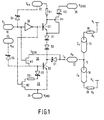
- Figure 1 shows a driver circuit which is connected between an input terminal 10 (V I ) and an output terminal 12 (V O ).
- the output terminal is shown connected to an intermediate point on a bus line 13 which is modelled in Figure 1 by transmission lines 14 and 16, terminated by respective resistors 18 and 20.
- the transmission lines 14 and 16 have a characteristic impedance Z 0 , while the terminating resistors 18 and 20 connect the bus line to a terminating voltage V t with a resistance R t each.
- the output terminal 12 (V O ) may be an output pin of an integrated circuit package including the driver circuit, and also a connector for making the connection to the bus line 13.
- the driver circuit has two main supply terminals 22 (V CC ) and 24 (V GND ) and a bias supply terminal 26 (V BIAS ).
- the supply terminals 22, 24 and 26 may be the supply pins of the integrated circuit package, which may include several similar driver circuits. Between the supply terminal 22 (V CC ) and the supply terminal 24 V( GND ), there are connected in series: a first resistor R1, an upper NPN transistor Q1, two p-n didoes D1 and D2 and a lower NPN transistor Q2.
- the NPN transistors Q1 and Q2 have their emitters towards terminal 24 (V GND ) and the diodes D1 and D2 have their cathodes towards terminal 24 (V GND ).
- the collector of the lower NPN transistor Q2 is connected to the cathode of a first Schottky diode S1, whose anode is connected to the output terminal 12 (V O ).
- the inverter terminal 10 (V I ) is connected to the input of a CMOS inverter 28 and also to the gate of an N-channel insulated gate field-effect transistor N1.
- CMOS complementary metal-oxide-semiconductor
- the drain of transistor N1 is connected to the output terminal 12 (V O ), while the source of transistor N1 is connected to the base of the lower NPN transistor Q2.
- the devices N1, Q2 and S1 together form a lower drive arrangement 30 of the driver circuit.
- the output of the inverter 28 is connected to the base of the upper NPN transistor Q1 and also to the gate of a further N-channel insulated gate transistor N2.
- the drain of transistor N2 is connected to the base of the lower NPN transistor Q2 via a second resistor R2 and a second Schottky diode S2 (cathode to R2).
- the source of transistor N2 is connected to the supply terminal 24 (V GND ).
- the devices N2, R2 and S2 form a base pull-off arrangement 32 for the lower NPN transistor Q2.
- a P-channel insulated gate transistor P1 has its source and gate connected to the emitter and collector respectively of the upper NPN transistor Q1.
- the collector of transistor Q1 is connected to the bias supply terminal 26 (V BIAS ) via a third Schottky diode S3.
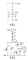
- Figure 2 shows the voltage levels V CC , V GDN and so forth that are present in normal operation in a version of the Figure 1 circuit suitable for use as a backplane driver in a Futurebus+ system.
- This version of the circuit is presented by way of example only. The invention is in no way limited to application in Futurebus+ or any other standard bus system.
- a positive bias voltage V BIAS equal to V CC , is applied to the terminal 26.
- the P-channel transistor is turned off (non-conducting), so that the elements P1 and S3 may be ignored.
- the elements P1 and S3 play a role in the "live insertion" of the driver circuit, to be described below with reference to Figure 3.
- the driver circuit receives at its input 10 a logic signal V I at conventional CMOS levels, and produces at its output 12 a corresponding inverted output signal V O at the logic levels of the Futurebus+ system.
- a threshold voltage V TH 1.55V is used by receiver circuits connected to the bus line 13 to distinguish between logic levels.
- the standard in fact specifies the following tolerance ranges (min,max): V OL (0.75,1.1V); V OH (1.9V,2.0V); V TH (1.47V, 1.62V); V CC (4.5V, 5.5V).
- the output of the inverter 28 is high (V CC ). Then the transistor N1 is turned off, while the transistor N2 and the upper NPN transistor Q1 are both turned on (conducting). In this state, therefore, the pull-off arrangement 32 actively turns off the lower NPN transistor Q2.
- the Schottky diode S2 has a characteristic forward voltage drop V S2 which is slightly less than the characteristic base-emitter forward voltage V BE of the NPN transistor Q2. This will improve switching speed in a subsequent transition to the V OL state, since the capacitance inherent in the base of transistor Q2 need only be changed from V S2 to VBE before the NPN transistor Q2 will turn on.
- the transistor Q1 is conducting and the diodes D1 and D2 are forward biased.
- the voltage drop from V CC across the transistor Q1 and the diodes D1 and D2 means that the cathode of the output Schottky diode S1 is pulled up to a voltage around 3V, that is, somewhere between V OH and V CC .
- the output Schottky diode S1 is therefore reverse biased and, since the transistor Q2 is turned off, no static current flows in the driver circuit in the V OH state.
- the circuit In the V OH state, the circuit is essentially passive, the bus line 13 being held at V OH by the terminating voltage V t acting via the terminating resistors 18 and 20.
- the capacitance C S1 of the output pin 12 In a transition from the V OL state to the V OH state, the capacitance C S1 of the output pin 12, to assist a rapid transition on the bus line 13.
- FIG 3 shows C S1 and other capacitances present in the driver circuit of Figure 1.
- the transistor Q2 has a large effective collector emitter capacitance C Q2 due to its large size and the Miller effect which multiplies the actual collector-base capacitance by the current gain ⁇ (beta) of the transistor.
- This large capacitance C Q2 is decoupled from the output pin 12 in the V OH state by the smaller capacitance C C1 of the reverse biased output Schottky diode S1.
- ESD electrostatic discharge
- the ESD device E1 has a parasitic capacitance C E1 , which is not enhanced by the Miller effect because of the base-emitter connection. Also present is the capacitance C P inherent in the output pin 12, and the connections from it to the bus line 13.
- the total output capacitance C O of the driver circuit is approximately C S1 +C E1 +C P , and in particular does not include the large capacitance C Q2 of the lower NPN transistor Q2.
- the circuit can therefore be designed to have low output capacitance C O .
- a maximum of C O 5 picofarads (5pF) is specified for the Futurebus+ system.
- the output voltage V O does nor reach V GND , however.
- the transistor N1 is designed to have a certain on-resistance R DSN1 which causes V O to limited at the desired level V OL (1.0V for Futurebus+), while I O settles to a static value IOL.
- the desired setting of V OL holds over a wide range of temperature, since the gain of the N-channel transistor N1 decreases as VBE of the NPN transistor Q2 decreases with increasing temperature.
- the driver circuit In the V OL state, the driver circuit has active control of the level on the bus line 13. This allows control to be taken by any one of many such circuits connected to the bus line 13 in a wired-AND configuration. The non-controlling circuits simply remain in the V OH state.
- the 150pF may for example comprise 100pF due to the bus line itself and 50pF due to ten other drivers being connected to the same bus line.
- the pins 12 (V O ) and 24 (V GND ) and the corresponding internal interconnections must be constructed to carry the large current.
- the static ground supply current through pin 24 (V GND ) might reach 700-800mA accompanied by 7-8 watts of on-chip power dissipation.
- a circuit designed to cope with worst-case conditions might expect to supply I OL as high as 100mA.
- any additional on-chip power dissipation or current supply requirement for the circuit is very undesirable.
- the particular lower drive arrangement 30 in the circuit of Figure 1 contributes to a lower on-chip power dissipation.
- the connection of the drain of the N-channel transistor N1 to the output pin 12, beyond the output Schottky diode S1 results in the base current I Q2B (equal to I OL / ⁇ ) being drawn from the bus line 13, rather than from the chip's own positive supply terminal 22 (V CC ).
- a further benefit of drawing the base current for the transistor Q2 from the output terminal is that the positive supply terminal 22 (V CC ) needs to pass no significant static current, in either state. Only a transient current is drawn during the transition from the V OL state to the V OH state.
- driver circuit many variations are possible around the basic driving arrangement 30. Such variations will inevitably result when such a driving arrangement is adapted to different applications other than the Futurebus+ backplane.
- the polarities of the various transistors and diodes may be reversed, different voltage levels and current requirements may arise, and so forth.
- a complementary pair of such driving arrangements may be desirable in another application.
- the circuit need not be constructed in BiCMOS technology.
- the N-channel base control transistor N1 could be replaced by bipolar transistor, although this might require a very small base current to be drawn from V CC or from the input terminal 10.
- FIG 4 shows the driver circuit of Figure 1 (referenced 40 in Figure 4) as part of a larger circuit module 42, which makes use of the driver circuit's features for so-called live insertion.
- the terminals and signals of the driver circuit 40 are identified by the same reference signs as in Figure 1.
- the module 42 may for example comprise a single integrated circuit, a multi-chip package or a printed circuit board.
- the module 42 is connected in operation to other modules via bus system in the form of a backplane 44, and is removably connected to the backplane 44 by a connector 46 having mating pairs of contacts suffixed "a" and "b".
- the backplane 44 includes the bus line 13 of Figure 1, and supply lines 48 (V CC ') and 50 (V GND ').
- the bus line 13 may be unique in the backplane, carrying only serial data, or it may be just one of tens or hundreds of bus lines, carrying parallel data.
- a group of mating contact pairs 52a/52b is provided for connecting the module 42 to the V CC ' supply line 48 of the backplane.
- Another group of mating contact pairs 54a/54b is provided for connecting the module 42 to the V GND ' supply line 50.
- a single contact pair 56a/5b connects the module 42 to the bus line 13.
- the contact pair 58a/58b and at least one of the contact pairs in the group 54a/54b are constructed so as to make contact before the contact pairs 52a/52b and 56a/56b during mating of the connector 46.
- the connector 46 is shown in Figure 4 in an intermediate state of insertion in which only the contact pairs 58a/58b and at least one of the group 54a/54b are mated.
- the driver circuit 40 Within the circuit module 42 the driver circuit 40, a receiver circuit 60 and a data processing (DP) circuit 62 are all connected for operation to module supply lines 64 (V CC ) and 66 (V GND ).
- the V GND supply line 66 s connected directly to the contacts 54a of the connector 46, while the V CC supply line 64 is connected to the contacts 52a through a switch 68.
- the bias supply terminal 26 (V BIAS ) of the driver circuit 40 is connected to the contact 58a.
- the DP circuit 62 is connected to receive data from the contact 56a (bus line 13) via the receiver circuit 60.
- the DP circuit is connected for transmission of data to the input terminal 10 of the driver circuit 40, whose output 12 (V O ) is also connected to the contact 56a.
- Live insertion is the action of connecting the circuit module 42 to the backplane 44 while the backplane is active, and other modules (not shown) are communicating via the bus line 13.
- the main voltage supply lines 64 and 66 for the module 42 are connected via groups of contact pairs because of the supply currents for the module are too great for a single contact pair.
- the switch 68 is used to block the main supply currents during live insertion, since one contact pair in each group will inevitably mate first, and would otherwise be damaged or destroyed by the large current. The switch may be closed manually or automatically to activate the circuit module 42 once all contact pairs are fully mated.
- the bias supply terminal 26 (V BIAS ) of the driver circuit 40 is arranged to receive the bias voltage V BIAS independently of the main voltage supply V CC , and before contact is made with the bus line 13. This bias supply is used in the driver circuit 40 to pre-bias the output 12 of the driver circuit as follows.
- V GND a common level
- V CC supply pin 22 is assumed to be at V GND .
- Leakage through insulation or atmosphere will generally ensure this state.
- additional Schottky diodes S4 and S5 can be added as shown by broken lines in Figure 1, where they will discharge respective nodes in the circuit almost to V GND without affecting normal operation.
- the total output capacitance will be seen to comprise a first component (chiefly C S1 ) in series with a second component.
- the current from the V BIAS pin 26 also charges the capacitive voltage divider formed by these two components of the output capacitance C O .
- C S1 is designed to be approximately equal to C E1 +C P
- the P-channel transistor P1 turns off, allowing normal operation of the driver circuit to commence. Since the collector of the lower transistor Q2 is pre-charged to the voltage V C , above V OH , the circuit is essentially already in the passive, V OH state. Thus the module 42 can commence receiving data from the bus line 13 without introducing any further noise to the system.
- the Schottky diode S3 serves a further purpose in addition to its role in setting V C . If the live insertion facility is not in use, or if the V BIAS supply fails, either the Schottky diode S3 or the transistor P1 will isolate the V BIAS terminal 26 from the rest of the circuit whether that terminal is tied to V CC , tied to V GND , or left floating.
- the bias supply voltage V BIAS could be provided by a battery supply within the circuit module 42, rather than by a special arrangement of contacts in the backplane connector 46.
- the pre-charging of the various capacitances can be adjusted to allow low-noise live insertion in a given application. The voltage drops in the pre-charging current path can be altered as required, and also the capacitances if necessary, subject of course to other constraints.
- the capacitance of a diode such as the Schottky diode S1 can be altered by varying the size or nature of the device itself and/or by varying the size of the reverse bias voltage applied to the diode during the pre-charging.
Landscapes
- Engineering & Computer Science (AREA)
- Computer Hardware Design (AREA)
- Physics & Mathematics (AREA)
- Computing Systems (AREA)
- General Engineering & Computer Science (AREA)
- Mathematical Physics (AREA)
- Logic Circuits (AREA)
- Electronic Switches (AREA)
- Dc Digital Transmission (AREA)
Claims (8)
- Système de bus comprenant au moins une ligne de bus de données et un module de circuit connecté de manière amovible à la ligne de bus de données, le module de circuit comprenant un circuit d'attaque de bus logique (40) comportant :caractérisé en ce que le module de circuit comprend des moyens de connecteur pour appliquer une tension de polarisation à une borne d'alimentation et pour connecter le module de circuit au bus, les moyens de connecteur étant propres à garantir que durant l'introduction sous tension la tension de polarisation entre en contact avec la borne d'alimentation de polarisation du circuit d'attaque avant que la borne de sortie n'entre en contact avec la ligne de bus, l'introduction sous tension étant une connexion physique du module de circuit à la ligne de bus de données alors que la ligne de bus de données est active, et en ce que le circuit d'attaque de bus logique contient des moyens de pré-polarisation (26, S3, P1, S1) connectés à la borne d'alimentation de polarisation et fonctionnant pour établir à la borne de sortie une tension pratiquement dans une plage de niveaux de tension qui sont pris par la ligne de bus en fonctionnement, avant que la borne de sortie n'entre en contact avec la ligne de bus durant l'introduction sous tension.une borne de sortie (12) connectée de manière amovible à la ligne de bus de données (13);une borne d'alimentation à connecter à une tension d'alimentation (GND), etdes moyens d'attaque (Q2, N1) pour connecter la borne de sortie à la borne d'alimentation pour le passage d'un courant de sortie sous le contrôle d'un signal d'entrée;
- Module de circuit à utiliser dans un système de bus, lequel système de bus comprend une ligne de bus de données (13), le module de circuit comprenant un circuit d'attaque de bus logique comportant :caractérisé en ce que le module de circuit comprend des moyens de connecteur pour appliquer une tension de polarisation à une borne d'alimentation et pour connecter le module de circuit au bus, les moyens de connecteur étant propres à garantir que durant l'introduction sous tension la tension de polarisation entre en contact avec la borne d'alimentation de polarisation du circuit d'attaque avant que la borne de sortie n'entre en contact avec la ligne de bus, l'introduction sous tension étant une connexion physique du module de circuit à la ligne de bus de données alors que la ligne de bus de données est active, et en ce que le circuit d'attaque de bus logique contient des moyens de pré-polarisation (26, S3, P1, S1) connectés à la borne d'alimentation de polarisation et fonctionnant pour établir à la borne de sortie une tension pratiquement dans une plage de niveaux de tension qui sont pris par la ligne de bus en fonctionnement, avant la connexion de la borne de sortie à la ligne de bus durant l'introduction sous tension.une borne de sortie (12) à connecter à la ligne de bus de données (13);une borne d'alimentation à connecter à une tension d'alimentation (GND), etdes moyens d'attaque (Q2, N1) pour connecter la borne de sortie à la borne d'alimentation pour le passage d'un courant de sortie sous le contrôle d'un signal d'entrée;
- Module de circuit suivant la revendication 2, propre à désactiver les moyens de pré-polarisation au terme d'une introduction sous tension.
- Module de circuit suivant la revendication 2, comprenant :et dans lequel :une autre borne d'alimentation (22) à connecter à une autre tension d'alimentation (Vcc), etd'autres moyens d'attaque (Q1) connectés entre l'autre borne d'alimentation et les moyens d'attaque et fonctionnant pour fournir un autre courant à un noeud entre les moyens d'attaque et les autres moyens d'attaque,les moyens de pré-polarisation fonctionnent pour établir ladite tension à la borne de sortie avant la connexion de l'autre borne d'alimentation sur l'autre tension d'alimentation durant l'introduction sous tension.
- Module de circuit suivant la revendication 2, dans lequel les moyens de pré-polarisation comprennent une diode de sortie (S1) comportant une cathode connectée aux moyens d'attaque et comportant une anode connectée à la borne de sortie.
- Module de circuit suivant la revendication 5, dans lequel les moyens de pré-polarisation sont propres à appliquer une polarisation inverse à la diode de sortie (S1) avant connexion physique de la borne de sortie.
- Module de circuit suivant la revendication 3, dans lequel les moyens de pré-polarisation comprennent un transistor (P1) comportant un trajet de courant principal couplé entre la borne de polarisation et les moyens d'attaque et comportant une électrode de commande pour recevoir une tension d'arrêt au terme de l'introduction sous tension.
- Module de circuit suivant la revendication 7, comprenant :et dans lequel :une autre borne d'alimentation (22) à connecter à une autre tension d'alimentation (VCC), etd'autres moyens d'attaque (Q1) connectés entre l'autre borne d'alimentation et les moyens d'attaque et fonctionnant pour fournir un autre courant à un noeud entre les moyens d'attaque et les autres moyens d'attaque,le trajet de courant principal du transistor (P1) est connecté en parallèle aux autres moyens d'attaque (Q1), etl'électrode de commande du transistor (P1) est connectée à l'autre borne d'alimentation.
Applications Claiming Priority (2)
| Application Number | Priority Date | Filing Date | Title |
|---|---|---|---|
| US07/558,935 US5132564A (en) | 1990-07-27 | 1990-07-27 | Bus driver circuit with low on-chip dissipation and/or pre-biasing of output terminal during live insertion |
| US558935 | 1990-07-27 |
Publications (2)
| Publication Number | Publication Date |
|---|---|
| EP0468583A1 EP0468583A1 (fr) | 1992-01-29 |
| EP0468583B1 true EP0468583B1 (fr) | 2001-06-20 |
Family
ID=24231604
Family Applications (1)
| Application Number | Title | Priority Date | Filing Date |
|---|---|---|---|
| EP91201893A Expired - Lifetime EP0468583B1 (fr) | 1990-07-27 | 1991-07-18 | Circuit excitateur |
Country Status (5)
| Country | Link |
|---|---|
| US (1) | US5132564A (fr) |
| EP (1) | EP0468583B1 (fr) |
| JP (1) | JP3308564B2 (fr) |
| KR (1) | KR100264497B1 (fr) |
| DE (1) | DE69132642T2 (fr) |
Families Citing this family (13)
| Publication number | Priority date | Publication date | Assignee | Title |
|---|---|---|---|---|
| DE4133764C1 (fr) * | 1991-10-11 | 1993-02-18 | Texas Instruments Deutschland Gmbh, 8050 Freising, De | |
| JP3025118B2 (ja) * | 1992-10-26 | 2000-03-27 | 株式会社日立製作所 | 半導体集積回路装置と情報処理システム |
| EP1392028A1 (fr) * | 1993-11-29 | 2004-02-25 | Fujitsu Limited | Circuit d'attaque à portes complémentaires |
| JP3102253B2 (ja) * | 1994-03-18 | 2000-10-23 | 株式会社日立製作所 | メモリシステム |
| JP3598530B2 (ja) * | 1994-04-21 | 2004-12-08 | 株式会社日立製作所 | 活栓挿抜装置 |
| US5574865A (en) * | 1994-12-01 | 1996-11-12 | Unisys Corporation | System for data transfer protection during module connection/disconnection onto live bus |
| US5485107A (en) * | 1995-01-09 | 1996-01-16 | Unisys Corporation | Backplane driver circuit |
| US5696773A (en) * | 1996-04-25 | 1997-12-09 | Credence Systems Corporation | Apparatus for performing logic and leakage current tests on a digital logic circuit |
| US5959481A (en) * | 1997-02-18 | 1999-09-28 | Rambus Inc. | Bus driver circuit including a slew rate indicator circuit having a one shot circuit |
| JPH10326131A (ja) * | 1997-05-26 | 1998-12-08 | Nec Corp | バスドライバ |
| US6163202A (en) * | 1998-10-05 | 2000-12-19 | Lucent Technologies Inc. | Temperature compensation circuit for semiconductor switch and method of operation thereof |
| US6600356B1 (en) * | 1999-04-30 | 2003-07-29 | Analog Devices, Inc. | ESD protection circuit with controlled breakdown voltage |
| US6380772B1 (en) | 2000-05-17 | 2002-04-30 | Marvell International, Ltd. | Self-limiting pad driver |
Citations (1)
| Publication number | Priority date | Publication date | Assignee | Title |
|---|---|---|---|---|
| EP0352965A2 (fr) * | 1988-07-25 | 1990-01-31 | Ncr International Inc. | Système de transmission de données |
Family Cites Families (13)
| Publication number | Priority date | Publication date | Assignee | Title |
|---|---|---|---|---|
| US3614467A (en) * | 1970-06-22 | 1971-10-19 | Cogar Corp | Nonsaturated logic circuits compatible with ttl and dtl circuits |
| US4263645A (en) * | 1979-04-30 | 1981-04-21 | Gte Automatic Electric Laboratories, Inc. | Self-starting carrier subscriber power supply |
| US4415817A (en) * | 1981-10-08 | 1983-11-15 | Signetics Corporation | Bipolar logic gate including circuitry to prevent turn-off and deep saturation of pull-down transistor |
| JPS60177723A (ja) * | 1984-02-24 | 1985-09-11 | Hitachi Ltd | 出力回路 |
| US4746818A (en) * | 1985-03-12 | 1988-05-24 | Pitney Bowes Inc. | Circuit for maintaining the state of an output despite changes in the state of input |
| GB2185648A (en) * | 1985-12-04 | 1987-07-22 | Plessey Co Plc | Electronic interface circuit |
| JPS62154917A (ja) * | 1985-12-27 | 1987-07-09 | Hitachi Ltd | デジタル回路 |
| US4682050A (en) * | 1986-01-08 | 1987-07-21 | International Business Machines Corporation | Small signal swing driver circuit |
| FR2598871B1 (fr) * | 1986-05-14 | 1988-09-30 | Bendix Electronics Sa | Circuit d'interface bidirectionnel presentant un acces unipolaire et un acces bipolaire pour des signaux logiques |
| JPS63112893A (ja) * | 1986-10-28 | 1988-05-17 | Mitsubishi Electric Corp | 半導体集積回路 |
| KR960009249B1 (ko) * | 1987-04-24 | 1996-07-16 | 미다 가쓰시게 | 반도체 메모리 |
| JPH01251655A (ja) * | 1988-03-30 | 1989-10-06 | Matsushita Electron Corp | 半導体集積回路 |
| US5028809A (en) * | 1989-03-07 | 1991-07-02 | Hewlett-Packard Company | Computer bus structure permitting replacement of modules during operation |
-
1990
- 1990-07-27 US US07/558,935 patent/US5132564A/en not_active Expired - Fee Related
-
1991
- 1991-07-18 DE DE69132642T patent/DE69132642T2/de not_active Expired - Fee Related
- 1991-07-18 EP EP91201893A patent/EP0468583B1/fr not_active Expired - Lifetime
- 1991-07-24 KR KR1019910012656A patent/KR100264497B1/ko not_active Expired - Fee Related
- 1991-07-29 JP JP18847491A patent/JP3308564B2/ja not_active Expired - Fee Related
Patent Citations (1)
| Publication number | Priority date | Publication date | Assignee | Title |
|---|---|---|---|---|
| EP0352965A2 (fr) * | 1988-07-25 | 1990-01-31 | Ncr International Inc. | Système de transmission de données |
Also Published As
| Publication number | Publication date |
|---|---|
| KR920003660A (ko) | 1992-02-29 |
| EP0468583A1 (fr) | 1992-01-29 |
| JPH04298117A (ja) | 1992-10-21 |
| JP3308564B2 (ja) | 2002-07-29 |
| KR100264497B1 (ko) | 2000-09-01 |
| DE69132642T2 (de) | 2002-04-18 |
| US5132564A (en) | 1992-07-21 |
| DE69132642D1 (de) | 2001-07-26 |
Similar Documents
| Publication | Publication Date | Title |
|---|---|---|
| US5004936A (en) | Non-loading output driver circuit | |
| US4963766A (en) | Low-voltage CMOS output buffer | |
| US5198699A (en) | Capacitor-driven signal transmission circuit | |
| US7116128B2 (en) | Semiconductor device with bus terminating function | |
| US6249171B1 (en) | Method and apparatus for galvanically isolating two integrated circuits from each other | |
| US5532630A (en) | Receiver circuit with a bus-keeper feature | |
| EP0702860B1 (fr) | Protection contre les surtensions | |
| JPH04290008A (ja) | オフ・チップ・ドライバ回路 | |
| US6188247B1 (en) | Method and apparatus for elimination of parasitic bipolar action in logic circuits for history removal under stack contention including complementary oxide semiconductor (CMOS) silicon on insulator (SOI) elements | |
| US6040729A (en) | Digital output buffer for multiple voltage system | |
| US5132564A (en) | Bus driver circuit with low on-chip dissipation and/or pre-biasing of output terminal during live insertion | |
| US5654981A (en) | Signal transmission system and method of operation | |
| US4682054A (en) | BICMOS driver with output voltage swing enhancement | |
| US5994921A (en) | Universal sender device | |
| US5239211A (en) | Output buffer circuit | |
| JPH02222216A (ja) | BiCMOSドライバ回路 | |
| US5828231A (en) | High voltage tolerant input/output circuit | |
| JP3431774B2 (ja) | 混合電圧システムのための出力ドライバ | |
| US5438281A (en) | Semiconductor integrated circuit device and data processing system having an interface with reduced parasitic capacitance | |
| US5786709A (en) | Integrated circuit output driver incorporating power distribution noise suppression circuitry | |
| US4918329A (en) | Data transmission system | |
| US5057714A (en) | BiCMOS integrated circuit device utilizing Schottky diodes | |
| EP0452919A2 (fr) | Circuit intégré semi-conducteur Bi-MOS | |
| EP0735686B1 (fr) | Circuit de tampon CMOS à trois états | |
| US5430398A (en) | BiCMOS buffer circuit |
Legal Events
| Date | Code | Title | Description |
|---|---|---|---|
| PUAI | Public reference made under article 153(3) epc to a published international application that has entered the european phase |
Free format text: ORIGINAL CODE: 0009012 |
|
| AK | Designated contracting states |
Kind code of ref document: A1 Designated state(s): DE FR GB IT |
|
| 17P | Request for examination filed |
Effective date: 19920724 |
|
| 17Q | First examination report despatched |
Effective date: 19950724 |
|
| RAP3 | Party data changed (applicant data changed or rights of an application transferred) |
Owner name: KONINKLIJKE PHILIPS ELECTRONICS N.V. |
|
| GRAG | Despatch of communication of intention to grant |
Free format text: ORIGINAL CODE: EPIDOS AGRA |
|
| GRAG | Despatch of communication of intention to grant |
Free format text: ORIGINAL CODE: EPIDOS AGRA |
|
| GRAH | Despatch of communication of intention to grant a patent |
Free format text: ORIGINAL CODE: EPIDOS IGRA |
|
| GRAH | Despatch of communication of intention to grant a patent |
Free format text: ORIGINAL CODE: EPIDOS IGRA |
|
| GRAH | Despatch of communication of intention to grant a patent |
Free format text: ORIGINAL CODE: EPIDOS IGRA |
|
| GRAA | (expected) grant |
Free format text: ORIGINAL CODE: 0009210 |
|
| AK | Designated contracting states |
Kind code of ref document: B1 Designated state(s): DE FR GB IT |
|
| PG25 | Lapsed in a contracting state [announced via postgrant information from national office to epo] |
Ref country code: IT Free format text: LAPSE BECAUSE OF FAILURE TO SUBMIT A TRANSLATION OF THE DESCRIPTION OR TO PAY THE FEE WITHIN THE PRESCRIBED TIME-LIMIT;WARNING: LAPSES OF ITALIAN PATENTS WITH EFFECTIVE DATE BEFORE 2007 MAY HAVE OCCURRED AT ANY TIME BEFORE 2007. THE CORRECT EFFECTIVE DATE MAY BE DIFFERENT FROM THE ONE RECORDED. Effective date: 20010620 |
|
| REF | Corresponds to: |
Ref document number: 69132642 Country of ref document: DE Date of ref document: 20010726 |
|
| ET | Fr: translation filed | ||
| REG | Reference to a national code |
Ref country code: GB Ref legal event code: IF02 |
|
| PLBE | No opposition filed within time limit |
Free format text: ORIGINAL CODE: 0009261 |
|
| STAA | Information on the status of an ep patent application or granted ep patent |
Free format text: STATUS: NO OPPOSITION FILED WITHIN TIME LIMIT |
|
| 26N | No opposition filed | ||
| PGFP | Annual fee paid to national office [announced via postgrant information from national office to epo] |
Ref country code: FR Payment date: 20020724 Year of fee payment: 12 |
|
| PGFP | Annual fee paid to national office [announced via postgrant information from national office to epo] |
Ref country code: GB Payment date: 20020731 Year of fee payment: 12 |
|
| PGFP | Annual fee paid to national office [announced via postgrant information from national office to epo] |
Ref country code: DE Payment date: 20020918 Year of fee payment: 12 |
|
| PG25 | Lapsed in a contracting state [announced via postgrant information from national office to epo] |
Ref country code: GB Free format text: LAPSE BECAUSE OF NON-PAYMENT OF DUE FEES Effective date: 20030718 |
|
| PG25 | Lapsed in a contracting state [announced via postgrant information from national office to epo] |
Ref country code: DE Free format text: LAPSE BECAUSE OF NON-PAYMENT OF DUE FEES Effective date: 20040203 |
|
| GBPC | Gb: european patent ceased through non-payment of renewal fee |
Effective date: 20030718 |
|
| PG25 | Lapsed in a contracting state [announced via postgrant information from national office to epo] |
Ref country code: FR Free format text: LAPSE BECAUSE OF NON-PAYMENT OF DUE FEES Effective date: 20040331 |
|
| REG | Reference to a national code |
Ref country code: FR Ref legal event code: ST |