EP0468760A1 - Amplificateur à deux modes d'opération - Google Patents
Amplificateur à deux modes d'opération Download PDFInfo
- Publication number
- EP0468760A1 EP0468760A1 EP91306733A EP91306733A EP0468760A1 EP 0468760 A1 EP0468760 A1 EP 0468760A1 EP 91306733 A EP91306733 A EP 91306733A EP 91306733 A EP91306733 A EP 91306733A EP 0468760 A1 EP0468760 A1 EP 0468760A1
- Authority
- EP
- European Patent Office
- Prior art keywords
- current
- output
- amplifier
- transistor
- coupled
- Prior art date
- Legal status (The legal status is an assumption and is not a legal conclusion. Google has not performed a legal analysis and makes no representation as to the accuracy of the status listed.)
- Granted
Links
- 239000003990 capacitor Substances 0.000 claims description 8
- 230000004044 response Effects 0.000 claims description 8
- 238000012358 sourcing Methods 0.000 claims description 6
- 238000000034 method Methods 0.000 claims description 2
- 239000004020 conductor Substances 0.000 claims 4
- 238000010586 diagram Methods 0.000 description 6
- 229920006395 saturated elastomer Polymers 0.000 description 4
- 230000007423 decrease Effects 0.000 description 2
- 230000003213 activating effect Effects 0.000 description 1
- 230000001276 controlling effect Effects 0.000 description 1
- 230000003111 delayed effect Effects 0.000 description 1
- 238000004519 manufacturing process Methods 0.000 description 1
- 230000001105 regulatory effect Effects 0.000 description 1
- 238000009877 rendering Methods 0.000 description 1
Images


Classifications
-
- H—ELECTRICITY
- H03—ELECTRONIC CIRCUITRY
- H03F—AMPLIFIERS
- H03F3/00—Amplifiers with only discharge tubes or only semiconductor devices as amplifying elements
- H03F3/45—Differential amplifiers
-
- H—ELECTRICITY
- H03—ELECTRONIC CIRCUITRY
- H03F—AMPLIFIERS
- H03F1/00—Details of amplifiers with only discharge tubes, only semiconductor devices or only unspecified devices as amplifying elements
- H03F1/02—Modifications of amplifiers to raise the efficiency, e.g. gliding Class A stages, use of an auxiliary oscillation
- H03F1/0205—Modifications of amplifiers to raise the efficiency, e.g. gliding Class A stages, use of an auxiliary oscillation in transistor amplifiers
- H03F1/0261—Modifications of amplifiers to raise the efficiency, e.g. gliding Class A stages, use of an auxiliary oscillation in transistor amplifiers with control of the polarisation voltage or current, e.g. gliding Class A
Definitions
- the present invention relates to amplifiers and, more particularly, to monolithic integrated differential and operational amplifiers.
- Monolithic differential and/or operational amplifiers are utilized in myriad of applications as is well understood.
- it has been a goal to produce amplifiers with low quiescent power consumption but such prior art amplifiers have been defficient in in output drive current and alternating current (AC) performance.
- AC alternating current
- portable battery powered applications such as mobile telephones, consumer entertainment systems e.g., radios and video games etc., it is especially important to limit the quiescent power consumption of amplifiers used in such applications.
- high output current operational amplifiers are comprised of an input stage that is coupled to an output stage.
- the operational amplifier In response to an alternating input signal being applied to the input stage, the operational amplifier both sources and sinks drive current to and from a load coupled to the output stage.
- the input and output stages are biased to a quiescent drain current to permit quality audio and data processing applications.
- low power, high output current amplifiers such as the MC 33178 manufactured by Motorola, Inc. draw approximately 420 microamperes of drain current per amplifier in the quiescent operating mode with no input signal applied thereto.
- micropower and battery powered applications there is a need to reduce drain current requirements over the foregoing while providing amplifiers that can supply high load currents.
- an amplifier having an input and output stage for providing drive current to a load coupled thereto which comprises circuitry that senses when an input signal is applied to the amplifier and is responsive thereto for providing an enabling signal at an output thereof and current regulator circuitry that supplies a low drain current to bias the input and output stages when the amplifier is in a quiescent operating mode absent an applied input signal and that is responsive to the enabling signal for increasing the current supplied to said input and output stages to bias the same in a high bias drain current operating mode.
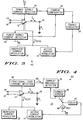
- Figs. 1-3 there are shown three embodiments of the amplifier of the present invention including an operational amplifier having two operating modes in accordance with the teachings herein.
- Amplifiers 10, 30 and 40 each include circuitry responsive to an applied input signal for operating the operational amplifier in a high drain bias current mode and in the absence of an applied input signal maintaining the operational amplifier in a low drain bias current quiescent operation mode. It is understood that the amplifiers are suited to be manufactured in integrated circuit form using, for example, conventional bipolar fabrication processes. In addition, like components between Figures are designated by the same reference numerals.
- amplifier 10 comprising a conventional operational amplifier 12 and additional associated circuitry for controlling the operating state of the operational amplifier by placing the operational amplifier in either a low quiescent drain current mode ("sleep mode”) or a high drain current mode (“awake mode”) of operation, i.e., a two state operated amplifier.
- operational amplifier 12 is responsive to an input signal applied at differential inputs 14 and 16 for supplying a high drive current, I L , at output 18 to a load R L .
- operational amplifier 12 includes a differential input stage for receiving the differential input signal, an intermediate stage coupled between the input stage and an output stage the latter of which is coupled to output 18 for both sinking and sourcing the load current.
- Amplifier 10 further includes regulating circuitry comprising quiescent current regulator 20 and active current regulator 22 for supplying the bias current I Bias to the stages of operational amplifier 12.
- a voltage comparator 24 is coupled to the respective inputs 14 and 16 of amplifier 10 and has an output coupled to enable circuitry 26 the latter of which has an output coupled to an enable input of active current regulator 22.
- amplifier 10 In operation, in the absence of an applied input signal, amplifier 10 is biased in the "sleep" or quiescent operating mode. In this sleep mode, active current regulator is disabled and only quiescent current regulator 22 supplies a low drain current I Bias for biasing the particular stages of operational amplifier 12.
- the magnitude of the quiescent or sleep mode drain current may be on the order of 20 microamperes. This is sufficient bias drain current to maintain the amplifier functional in order to respond to the input signal.
- voltage comparator 24 detects the presence of a differential input signal at the inputs of amplifier 10 it supplies a control signal for activating enable circuitry 26. As enable circuitry 26 is activated an enable signal is supplied to active current regulator 22.
- active current regulator 22 sinks additional bias current to increase the magnitude of I Bias to a higher bias drain current level to operate the stages in the higher "awake” or active mode to supply the high output current to load R L .
- amplifier 30 of the preferred embodiment which operates in the two operating modes as described above with respect to amplifier 10.
- Amplifier 30 is responsive to the input signal applied to inputs 14 and 16 and senses a current that is proportional to a change in the load current I L by current detector 28 which is coupled to the output stage of operational amplifier 12 to control the operation of enable circuitry 26.
- active current regulator 22 is enabled in response to an applied input signal causing the load current I L to exceed a predetermined threshold value.
- amplifier 40 of Fig. 3 operates in a sleep mode and an awake mode in substantially the same manner as described for the amplifiers of Figs. 1 and 2.
- a change in the power supply current is detected by detector 32 responsive to an input signal applied to inputs 14 and 16 rendering the output stage of operational amplifier active to begin to source load current.
- Detector 32 being coupled between the positive power supply rail to which Vcc is supplied and operational amplifier 12 senses an increase in the power supply current drain due to the input signal. This increase in current is compared to a reference current by current comparator 36 such that a control signal is generated to enable circuitry 26 to enable regulator 22.
- detector 34 senses a change in current in the negative supply rail. This change is detected by current comparator 36 to enable regulator 22 as before.
- amplifier 50 (which is a more detailed block and schematic diagram of amplifier 30) is shown to more fully explained the preferred embodiment of the invention.
- a fractional load current detector 42 coupled to the output stage of operational amplifier 12, is utilized to sense the load current therethrough to provide an output current at its output that is proportional to a fraction of the load current.
- the output of detector 42 is coupled to an input of current threshold detector 44.
- Current threshold detector 44 has an additional input terminal coupled to an input of current mirror 46 the output of which is coupled both to reference current supply 48 and an input of delay circuit 52.
- An output of delay circuit is coupled to the enable input of active current regulator 22.
- quiescent current regulator 20 is activated to supply quiescent drain bias current through the stages of operational amplifier 12.
- I Bias is at some nominal value, eg., 20 microamperes.
- This sleep mode of operation of amplifier 50 therefore requires minimum drain bias current, sufficient to permit operational amplifier 12 to be responsive to an input signal applied to inputs 14 and 16. Since there is no load current during the sleep mode of operation the output of detector 42 is essentially zero. Current threshold detector 44 therefore remains in the low drain current state and does not supply an input current to current mirror 46; hence, I D is zero.
- Delay circuit 48 is thus rendered inoperative and does not supply an enabling signal to current regulator 22.
- load current I L will begin to be either sourced or sank at output 18.
- Detector 42 senses a fraction of this load current and provides an output current, %I L , that is proportional to the actual current I L .
- %I L an output current
- input current is supplied to current mirror 46.
- Current mirror 46 will then source the current I D at its output. Once the magnitude of I D exceeds I REF delay circuit 52 will become operative to supply an enabling signal to active current regulator 22.
- bias current I Bias is then supplied to bias operational amplifier 12 in the high drain bias state and the operational amplifier is then in an awake mode to supply high output load current in a conventional manner.
- the enabling signal provided by delay circuit 52 will remain on for a predetermined time, is delayed, after the input signal becomes zero. This will prevent distortion in the output signal whenever the alternating input signal crosses zero between alternating half-cycles.
- Operational amplifier section 12 of the amplifier is shown as including a differential input stage 60 for receiving differential input signals at inputs 14 and 16 and providing a single ended output signal to an intermediate stage comprising transistor 64 and resistor 66 the latter of which is coupled between the emitter of the former and negative supply rail V EE .
- Transistor 64 is configured as an emitter-follower having its collector coupled to current supply 80.
- the collector and emitter of transistor 64 are coupled to respective inputs of the output stage of operational amplifier 12 comprising load current sinking output transistor 68, diode 70, series connected diodes 76 and 78 and current sourcing output transistor 74 all of which are interconnected in a known manner.
- Both current sinking transistor 68 and current sourcing transistor 74 of the output stage are coupled to output terminal 18 through resistor 72.
- operational amplifier is conventional in structure with the several stages thereof being biased in a quiescent bias or sleep mode by current regulator 20 as will be now described.
- Current regulator 20 comprising cross coupled transistors 94 and 96, resistors 100 and 102, diode 104 and output transistors 106, 108 and 110 is well known.
- U. S. Patent No. 4,491,780 teaches the structure and operation of both regulator 20 and 22. Briefly, a ⁇ V BE voltage is established across resistor 100 which sets the output current flowing through the collector-emitter conduction paths of transistors 106, 108 and 110.
- the quiescent bias drive current I Bias is supplied to the appropriate stages of operational amplifier 12 through transistors 106 and 108.
- the collector of transistor 106 is coupled to a current mirror comprising diode-connected transistor 88 and transistor 86.
- current mirror 80 comprised of diode-connected transistor 84 and transistor 82, is responsive to transistor 108 sinking current from transistor 84 to supply quiescent bias current from the collector of transistor 82 to the collector of transistor 64 as well as the output stage to supply quiescent current therethrough
- input stage 60 renders emitter-follower transistor 64 conductive to sufficiently allow transistor 68 to be turned on.
- Devices 70, 74, 76 and 78 are ideally matched.
- I L being zero
- the sum of the voltage drop across the base-emitter of transistor 74 and diode 70 is equal to the sum of the voltage drop across diodes 76 and 78.
- Fractional load current detector 42 is illustrated as including four sensing transistors 128, 130, 132 and 134 and respective resistors R as well as current mirrors 136, 138, 142 and 144.
- transistors 128 and 130 are utilized to sense the presence of load current being sourced to output 18 via transistor 74 and resistor 72 while transistors 132 and 134 sense load current flow from output 18 through transistor 68.
- the bases of transistors 128 and 130 are commonly connected at the anode of diode 76 and the base of output transistor 74 while the emitter of the transistor 128 is connected via resistor R to the anode of diode 78 and the emitter of transistor 130 is coupled via respective resistor R to the anode of diode 70.
- the collector of transistor 128 is returned to the input of a current mirror formed by multi-collector transistor 136 in a conventional manner, the output of the current mirror (the second collector of transistor 136) being coupled to node 140 and to the collector of transistor 130.
- Node 140 is also coupled to the input of the current mirror formed by multi-collector transistor 138 the output of which is connected to node 148.
- the base-emitter of transistor 132 is coupled, via resistor R, across diode 78 while the base-emitter of transistor 134 is coupled across diode 70 via resistor R.
- the collector of transistor 132 is coupled to the input (the first collector of transistor 142) of the current mirror formed by multi-collector transistor 142 the output of the latter being coupled both to the collector of transistor 134 and the input of the current mirror formed by multi-collector transistor 144.
- the output of the current mirror formed by transistor 144 is connected in common at node 148 to the output of the current mirror formed by transistor 138 and to the input of current threshold detector or switch 44 at the emitter of transistor 150.
- Current threshold detector 44 includes multi-collector transistor 150 the emitter of which is coupled to node 148 as well as one output of current mirror 178.
- a first collector of transistor 150 is interconnected to its base and is coupled both to the negative supply rail via diode 152 and to the base of transistor 162.
- the collector of transistor 162 is coupled to the input of current mirror 46 the output of the latter being coupled to current reference source 48, the emitter of transistor 162 is coupled to the output of current mirror 160 (which supplies a constant current) while the input of the current mirror is coupled to an output of current mirror 112.
- One output of current mirror 178 is coupled to the input node 66 of regulator 22 while its input is coupled to the collector of transistor 176 of delay circuit 52.
- Delay circuit 52 further includes transistor 170 the base of which is coupled both to the output of the current mirror forming current reference 48 and to the output of current mirror 46 while its emitter is coupled to the base of transistor 174 and one electrode of capacitor 172, the other electrode of which is returned to V EE .
- the collectors of transistors 170 and 174 are returned to V CC and the emitter of transistor 174 is coupled both to the base of transistor 176 and the base of transistor 180.
- the emitter of transistor 176 is coupled to an output of current mirror 48.
- the collector of transistor 180 is returned to V CC while its emitter is coupled with the base of transistor 170 to the other output of current mirror 48.
- the bias current flowing through transistor 74 equals that flowing through diode 76 and similarly the current through diode 70 is equal to that of diode 78.
- transistors 128 and 130 are equally biased such that the current mirrored at the second collector of transistor 136, due to the current sank at its interconnected collector and base by transistor 128, is completely sank by transistor 130.
- no current is mirrored by current mirror transistor 138 to node 148.
- current mirror transistor 144 remains inactive as no base current is sourced therefrom as transistor 134 will sink all of the current sourced from transistor 142, due to transistor 132, and no current is mirrored to node 148 from the output collector of transistor 144.
- a unique feature of current detector circuit 42 is to subtract out the quiescent current from the fractional load current that is detected. Since no current is source to node 148 from current detector 42 when the load current is zero (either if the amplifier is in a sleep mode or awake mode), transistor 150 is rendered non-conductive and current threshold detector 44 is inactive. In this state transistor 162 is non-conductive and does not sink input current from current mirror 46. However, as current mirror 112 has input current supplied thereto through transistor 110, an output current is sourced to the input of current reference 48 which in turns wants to sink the current I REF at its outputs. Because current mirror 46 is inactive, I D is zero whereby delay circuit 52 is also inactive as transistor 170 remains in an off condition since there is no base current drive available thereto. Hence, transistors 174, 176 and 180 will be turned off. Since there is no input current supplied to current mirror 178 in this condition active current regulator will remain in a disabled state as there is no output current supplied to node 66 from current mirror 178.
- regulator 20 supplies the quiescent bias currents to the stages of operational amplifier 12. Since, there is no load current supplied at output 18, load current detector provides no current output to current threshold detector 44 which is thus rendered inactive which in turn disables delay circuit 52. Hence, operational amplifier 12 is maintained in a sleep mode since current regulator 22 is disabled but is ready to respond to an applied input signal while drawing minimum bias current.
- amplifier 50 will be placed in an awake mode by active current regulator being enabled to provide additional bias current to the stages of operational amplifier 12.
- either output transistor 68 will be turned harder on to sink current from output 18 during one half of the alternating input signal, and will tend to be turned off during the other half of the alternating input signal while output transistor 74 is turned harder on to source current to output 18.
- transistor 74 will tend to be turned off as base current drive thereto is shunted by transistor 68. Load current is thus sourced from output 18 through diode 70 which increases the voltage drop across the diode.
- sensing transistor 134 causes sensing transistor 134 to be turned on to also sink a fractional amount of the load current therethrough depending on the ratio of its emitter area with respect to the emitter area of the diode-connected transistor forming diode 70. For example, if diode 70 has an emitter area eight times greater than that of transistor 134, approximately one eighth of total load current flowing through transistor 68 flows through transistor 134 depending on the resistance of the resistor R. However, the voltage drop across diodes 76 and 78 remains constant. Hence, transistor 134 is more conductive than transistor 132 and wants to sink more current than can be supplied from the output of current mirror transistor 142 at its second collector.
- This additional current is however supplied by current mirror transistor 144 wherein the sum of the currents supplied by transistors 142 and 144 is equal to the fractional load current sunk by transistor 134. Transistor 144 mirrors this current to supply a current, proportional to the fractional load current, to node 148 and to current threshold detector 44.
- the current sourced to transistor 150 is evenly split between the collectors thereof and sourced to diode 152 and to the collector of transistor 154.
- transistor 154 remains saturated until the magnitude of the current sourced to node 148 increases to a predetermined value. For instance, if the emitter area of transistor 154 is made 4 times greater than the area of diode connected transistor 152, transistor 154 remains saturated until the voltage across resistors 156 and 158 reaches approximately 36 millivolts (depending on the resistances thereof). As long as transistor 154 is saturated, transistor 162 is biased off as all of the current is sank through the former.
- transistor 176 As soon as the voltage across capacitor 172 reaches a value to forward bias transistor 174 it begins to conduct thereby turning transistors 176 and 180 on. Transistor 176 then passes the input current sourced from current mirror 178 to current mirror 48. Current mirror 178 then supplies an output current to input node 66 which now enables active current regulator 22. As current regulator 22 is enabled additional bias current is supplied to the stages of operational amplifier 12 through transistors 124 and 126. Operational amplifier 12 is therefore placed in its active or awake mode of operation. In a like manner, on the alternating half cycle of the input signal to operational amplifier 12, transistor 74 is rendered more conductive in response to the input signal which causes transistor 130 to sink a fractional amount of the load current sourced to output 18.
- Transistor 130 will then will want to sink more current than is supplied by current mirror transistor 136.
- the additional current required by transistor is drawn from the bas-collector of transistor 138.
- Current mirror transistor 138 is thus rendered conductive to supply the additional collector current of transistor 130.
- the fractional load current sunk by transistor 130 is then mirrored by transistor 138 to node 148.
- the aforedescribed operation of current threshold detector is repeated on the alternating half cycle of the input signal. It is important to note that the enabling signal from delay circuit 52 is not interrupted as the input signal crosses from one alternating half-cycle to the next as capacitor 172 does not have time to discharge sufficiently to turn off transistor 176.
- capacitor 172 will discharge which eventually turns transistors 174, 176 and 180 off as the voltage across the capacitor decreases below the value needed to maintain the transistors in a forward biased condition to thereby remove the enabling signal from current mirror 178.
- Current regulator 22 will then become disabled and amplifier 50 is returned to its sleep mode as long as the operating potentials are supplied thereto.
- transistor 180 prevents transistor 170 from zenering as I D goes to zero while the voltage across capacitor 172 is at its peak value.
- hysteresis is provided to maintain current threshold detector 44 active until the output current from detector 42 falls below the value required to activate threshold detector 44. This hysteresis is provide by the additional current supplied to node 148 from the output of current mirror 178.
- delay circuit 52 As soon as delay circuit 52 is rendered operative the additional current will be supplied to the emitter of transistor 150 and, which due to the gain of the circuit, will quickly drive transistor 162 to a conducting state. Now, the magnitude of the current sourced to node 148 from load current detector circuit 42 must decrease below the predetermined value required to turn on transistor 162 before the latter can be turned off.
Landscapes
- Engineering & Computer Science (AREA)
- Power Engineering (AREA)
- Amplifiers (AREA)
Applications Claiming Priority (2)
| Application Number | Priority Date | Filing Date | Title |
|---|---|---|---|
| US558927 | 1990-07-27 | ||
| US07/558,927 US5059921A (en) | 1990-07-27 | 1990-07-27 | Amplifier having two operating modes |
Publications (2)
| Publication Number | Publication Date |
|---|---|
| EP0468760A1 true EP0468760A1 (fr) | 1992-01-29 |
| EP0468760B1 EP0468760B1 (fr) | 1996-04-24 |
Family
ID=24231571
Family Applications (1)
| Application Number | Title | Priority Date | Filing Date |
|---|---|---|---|
| EP91306733A Expired - Lifetime EP0468760B1 (fr) | 1990-07-27 | 1991-07-24 | Amplificateur à deux modes d'opération |
Country Status (7)
| Country | Link |
|---|---|
| US (1) | US5059921A (fr) |
| EP (1) | EP0468760B1 (fr) |
| JP (1) | JP2893429B2 (fr) |
| KR (1) | KR100222009B1 (fr) |
| DE (1) | DE69118984T2 (fr) |
| HK (1) | HK1000749A1 (fr) |
| SG (1) | SG46260A1 (fr) |
Cited By (1)
| Publication number | Priority date | Publication date | Assignee | Title |
|---|---|---|---|---|
| EP0986174A1 (fr) * | 1998-09-11 | 2000-03-15 | STMicroelectronics GmbH | Comparateur |
Families Citing this family (13)
| Publication number | Priority date | Publication date | Assignee | Title |
|---|---|---|---|---|
| KR930703742A (ko) * | 1990-12-17 | 1993-11-30 | 다니엘 케이. 니콜스 | 동적으로 바이어스된 증폭기 |
| FR2686757B1 (fr) * | 1992-01-29 | 1997-03-28 | Sgs Thomson Microelectronics | Modulateur du courant d'une ligne telephonique. |
| US5334948A (en) * | 1993-02-17 | 1994-08-02 | National Semiconductor Corporation | CMOS operational amplifier with improved rail-to-rail performance |
| US6043706A (en) * | 1999-02-05 | 2000-03-28 | Ericsson Inc. | Methods and apparatus for controlling power amplifier quiescent current in a wireless communication device |
| DE10056878A1 (de) * | 2000-11-16 | 2002-06-06 | Bosch Gmbh Robert | Ein stromfühlender Schalterstromkreis |
| JP3820918B2 (ja) * | 2001-06-04 | 2006-09-13 | セイコーエプソン株式会社 | 演算増幅回路、駆動回路、及び駆動方法 |
| JP3791354B2 (ja) | 2001-06-04 | 2006-06-28 | セイコーエプソン株式会社 | 演算増幅回路、駆動回路、及び駆動方法 |
| US7030690B2 (en) * | 2004-02-12 | 2006-04-18 | Honeywell International, Inc. | Operational amplifier with selectable performance characteristics |
| US8125572B2 (en) * | 2005-03-15 | 2012-02-28 | Maxim Integrated Products, Inc. | System and method for automatic power-up and power-down of an output video circuit |
| WO2008020368A2 (fr) * | 2006-08-15 | 2008-02-21 | Koninklijke Philips Electronics N.V. | Transmetteur hf avec amplificateur de puissance hf contrôlable |
| GB0715254D0 (en) * | 2007-08-03 | 2007-09-12 | Wolfson Ltd | Amplifier circuit |
| TWI449327B (zh) * | 2010-12-27 | 2014-08-11 | Novatek Microelectronics Corp | 運算放大器之偏壓電流控制方法及驅動電路 |
| CN106559054B (zh) * | 2012-05-24 | 2019-07-12 | 意法半导体研发(深圳)有限公司 | 具有增强的电流吸收能力的运算跨导放大器 |
Citations (3)
| Publication number | Priority date | Publication date | Assignee | Title |
|---|---|---|---|---|
| US3064202A (en) * | 1959-01-27 | 1962-11-13 | Gen Electric | Low current drain transistor amplifier |
| GB2084418A (en) * | 1980-09-16 | 1982-04-07 | Tokyo Shibaura Electric Co | Power amplifier |
| EP0094485A1 (fr) * | 1982-05-13 | 1983-11-23 | International Business Machines Corporation | Amplificateur différentiel à polarisation auto-adaptive |
Family Cites Families (3)
| Publication number | Priority date | Publication date | Assignee | Title |
|---|---|---|---|---|
| US4077013A (en) * | 1976-06-04 | 1978-02-28 | Norlin Music, Incorporated | Audio power amplifier with automatic bias control |
| JPS58133009A (ja) * | 1982-02-02 | 1983-08-08 | Nippon Gakki Seizo Kk | 電力増幅器 |
| IT1210936B (it) * | 1982-09-24 | 1989-09-29 | Ates Componenti Elettron | Amplificatore audio di potenza con regolazione automatica della corrente di polarizzazione assorbita dallo stadio finale. |
-
1990
- 1990-07-27 US US07/558,927 patent/US5059921A/en not_active Expired - Lifetime
-
1991
- 1991-07-23 KR KR1019910012575A patent/KR100222009B1/ko not_active Expired - Lifetime
- 1991-07-24 EP EP91306733A patent/EP0468760B1/fr not_active Expired - Lifetime
- 1991-07-24 SG SG1996001661A patent/SG46260A1/en unknown
- 1991-07-24 DE DE69118984T patent/DE69118984T2/de not_active Expired - Fee Related
- 1991-07-25 JP JP3207265A patent/JP2893429B2/ja not_active Expired - Fee Related
-
1997
- 1997-12-01 HK HK97102300A patent/HK1000749A1/en not_active IP Right Cessation
Patent Citations (3)
| Publication number | Priority date | Publication date | Assignee | Title |
|---|---|---|---|---|
| US3064202A (en) * | 1959-01-27 | 1962-11-13 | Gen Electric | Low current drain transistor amplifier |
| GB2084418A (en) * | 1980-09-16 | 1982-04-07 | Tokyo Shibaura Electric Co | Power amplifier |
| EP0094485A1 (fr) * | 1982-05-13 | 1983-11-23 | International Business Machines Corporation | Amplificateur différentiel à polarisation auto-adaptive |
Non-Patent Citations (3)
| Title |
|---|
| IEEE JOURNAL OF SOLID-STATE CIRCIUTS vol. 24, no. 3, June 1989, NEW YORK, US pages 744 - 746; R. KLINKE ET AL.: 'A Very-High-Slew-Rate CMOS Operational Amplifier ' * |
| PATENT ABSTRACTS OF JAPAN vol. 13, no. 470 (E-835)(3818) October 24, 1989 & JP-A-1 185 006 (HITACHI LTD ) July 24, 1989 * |
| PATENT ABSTRACTS OF JAPAN vol. 5, no. 63 (E-54)(735) April 28, 1981 & JP-A-56 12 111 (MATSUSHITA DENKI SANGYO K.K. ) February 6, 1981 * |
Cited By (2)
| Publication number | Priority date | Publication date | Assignee | Title |
|---|---|---|---|---|
| EP0986174A1 (fr) * | 1998-09-11 | 2000-03-15 | STMicroelectronics GmbH | Comparateur |
| US6323695B1 (en) | 1998-09-11 | 2001-11-27 | Stmicroelectronics Gmbh | Comparator with controllable bias current source |
Also Published As
| Publication number | Publication date |
|---|---|
| JP2893429B2 (ja) | 1999-05-24 |
| SG46260A1 (en) | 1998-02-20 |
| DE69118984T2 (de) | 1996-10-31 |
| US5059921A (en) | 1991-10-22 |
| DE69118984D1 (de) | 1996-05-30 |
| EP0468760B1 (fr) | 1996-04-24 |
| JPH0514064A (ja) | 1993-01-22 |
| HK1000749A1 (en) | 1998-04-24 |
| KR920003630A (ko) | 1992-02-29 |
| KR100222009B1 (ko) | 1999-10-01 |
Similar Documents
| Publication | Publication Date | Title |
|---|---|---|
| US5059921A (en) | Amplifier having two operating modes | |
| US3939399A (en) | Power circuit with shunt transistor | |
| US5966004A (en) | Electronic system with regulator, and method | |
| HK1000749B (en) | Amplifier having two operating modes | |
| US5642076A (en) | No turn-on pop noise amplifier | |
| US5307025A (en) | Audio power amplifier with noise prevention at turn-on and turn-off | |
| US5537081A (en) | No turn-on pop noise amplifier | |
| US5140280A (en) | Rail-to-rail output stage of an operational amplifier | |
| US4743833A (en) | Voltage regulator | |
| JPH03181868A (ja) | ピーク検出器 | |
| US10333478B1 (en) | Slew boost disable for an operational amplifier | |
| US5059923A (en) | Fractional load current detector | |
| JPH1124764A (ja) | 直流安定化電源装置 | |
| US5977829A (en) | Low distortion current feedback amplifier with dynamic biasing | |
| EP0483526B1 (fr) | Circuit pour détection de seuil de courant | |
| US10439570B2 (en) | Slew boost disable for an operational amplifier | |
| US6316995B1 (en) | Input stage for constant gm amplifier circuit and method | |
| US5332928A (en) | Battery drain reducer | |
| JPH05176255A (ja) | 電 源 | |
| US5764105A (en) | Push-pull output circuit method | |
| US4499432A (en) | Low voltage op amp bias optimizer | |
| JPH0576044B2 (fr) | ||
| JP2762466B2 (ja) | 可変減衰回路 | |
| JPH07306725A (ja) | 定電圧電源回路 | |
| JPH0518287B2 (fr) |
Legal Events
| Date | Code | Title | Description |
|---|---|---|---|
| PUAI | Public reference made under article 153(3) epc to a published international application that has entered the european phase |
Free format text: ORIGINAL CODE: 0009012 |
|
| AK | Designated contracting states |
Kind code of ref document: A1 Designated state(s): DE FR GB |
|
| 17P | Request for examination filed |
Effective date: 19920723 |
|
| 17Q | First examination report despatched |
Effective date: 19940726 |
|
| GRAA | (expected) grant |
Free format text: ORIGINAL CODE: 0009210 |
|
| AK | Designated contracting states |
Kind code of ref document: B1 Designated state(s): DE FR GB |
|
| PG25 | Lapsed in a contracting state [announced via postgrant information from national office to epo] |
Ref country code: FR Effective date: 19960424 |
|
| REF | Corresponds to: |
Ref document number: 69118984 Country of ref document: DE Date of ref document: 19960530 |
|
| EN | Fr: translation not filed | ||
| PLBE | No opposition filed within time limit |
Free format text: ORIGINAL CODE: 0009261 |
|
| STAA | Information on the status of an ep patent application or granted ep patent |
Free format text: STATUS: NO OPPOSITION FILED WITHIN TIME LIMIT |
|
| 26N | No opposition filed | ||
| REG | Reference to a national code |
Ref country code: GB Ref legal event code: 746 Effective date: 19990706 |
|
| PGFP | Annual fee paid to national office [announced via postgrant information from national office to epo] |
Ref country code: GB Payment date: 20010614 Year of fee payment: 11 |
|
| PGFP | Annual fee paid to national office [announced via postgrant information from national office to epo] |
Ref country code: DE Payment date: 20010731 Year of fee payment: 11 |
|
| REG | Reference to a national code |
Ref country code: GB Ref legal event code: IF02 |
|
| PG25 | Lapsed in a contracting state [announced via postgrant information from national office to epo] |
Ref country code: GB Free format text: LAPSE BECAUSE OF NON-PAYMENT OF DUE FEES Effective date: 20020724 |
|
| PG25 | Lapsed in a contracting state [announced via postgrant information from national office to epo] |
Ref country code: DE Free format text: LAPSE BECAUSE OF NON-PAYMENT OF DUE FEES Effective date: 20030201 |
|
| GBPC | Gb: european patent ceased through non-payment of renewal fee |
Effective date: 20020724 |